Idea
I have previously created a proof of concept for a simple 3x3 pixel image sensor using phototransistors. Feel free
to check it out here to understand the fundamentals and limitations of this type of sensor. In my last milestone, I
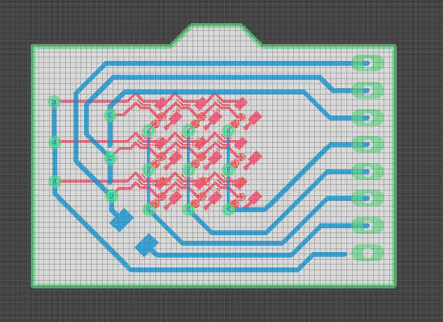
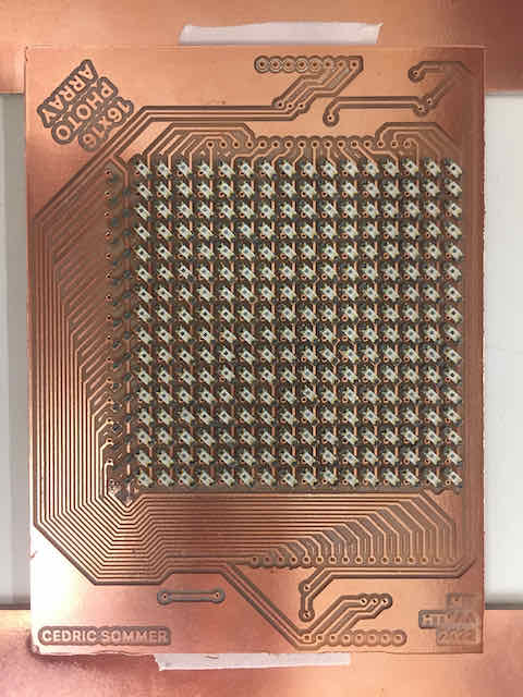
designed a larger image sensor with 16x16 phototransistors in Fusion 360, using a custom ULP automation script. The board design is an advanced double-sided board that will
push the limits of what you can DIY produce on an endmill. Now, we will execute this design and manufacture it on an endmill. We will then use a solder stencil and reflow soldering
to solder our 256 pixels. Last, we will take some first images using our image sensor to make sure all pixels work as intended.
This is the fifth milestone in a series of posts that cover my final project, where I will be creating a 16x16 pixel DSLR camera from scratch. In my case,
from scratch literally means milling the PCB for the electronics and stuffing it by hand, figuring out the optics and then putting everything into a nice
housing of 3d printed parts and flat panels. By the end, we will hopefully have a working model of a DSLR camera that can (natively!) produce cool pixel-art images
and demonstrates the inner workings of a modern-day DSLR camera.
Making a Scaled-Down Test Board (Summary)
Now, I have to admit, before I produced the final board design with 256 pixels, I felt it was a good idea to double-check if I could actually produce my board in the way
I envisioned. While I had previously created a 3x3 image sensor with a similar logic that worked, that one was soldered entirely by hand
and I did not create any vias. Basically, I wanted to go through all manufacturing steps I used for the first time (milling a double-sided board, laser-cutting a stencil from cardboard, using reflow soldering).
The following pictures give you a quick overview about the process, though I will save detailed explanations for the entire process and best practices for the
sections following, which describe the making of our final 16x16 image sensor. This is just a glance at what you're going to make! Don't be confused, the pattern is different from the one we will be using – I actually made this in
the process of designing my image sensor and later switched to a design with just phototransistors.
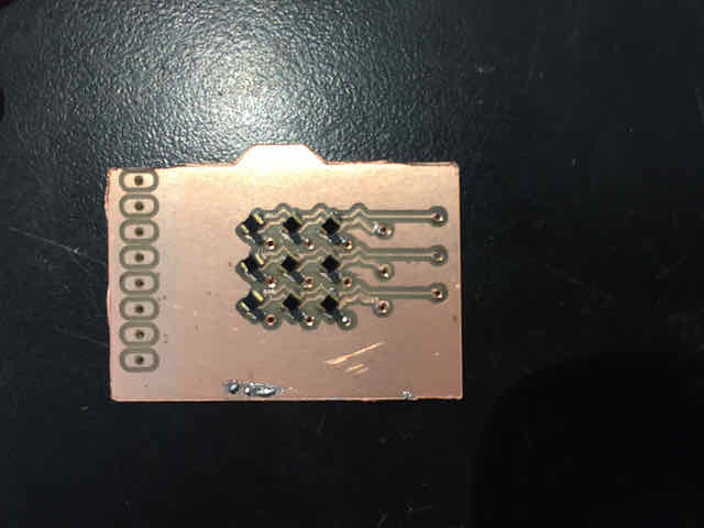
My 3x3 image board prototype – again, this is not the final pattern we will use
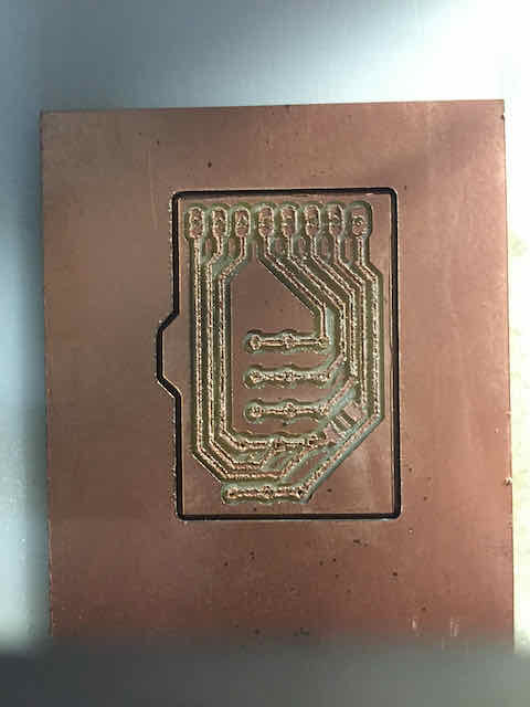
Milling the board on two sides and cutting it out
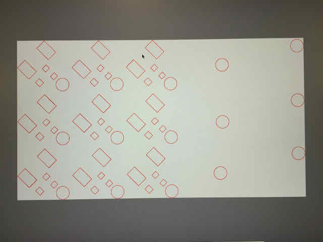
A stencil in Photoshop, which serves as a mask for our solder paste

I cut out the stencil under the laser cutter and lined it up with the board...
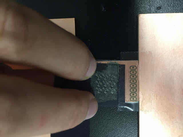
...and applied solder paste to check the results
Last, I tested stuffing and soldering my components using reflow soldering
This should give you a quick overview about what's to come. Let's dive in and learn about making our full-scale image sensor board.
Milling the Double-Sided Board
We ended our last milestone with exporting the files we can import for milling the traces, vias and outline. First, we have to generate the toolpaths for milling our board. As explained in Week 3, I will be using the desktop-sized Roland SRM-20 CNC in our
fab lab to mill the traces. I used Mods, a light in-browser toolpath generator developed by MIT's CBA, to generate my toolpath using the toolpaths from PNG template.
Before milling my board, I quickly checked if all files could be milled successfully by using the default milling settings, generating the toolpaths and seeing if two adjacent traces were not separated from each
other in the toolpaths. Luckily, all traces seemed fine and perfectly separated. If this weren't the case, I could have fixed things in Photoshop or go back to Eagle.

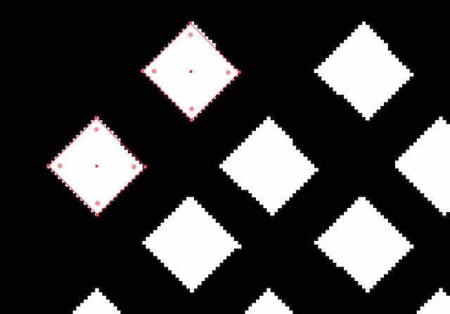
A quick check in Mods to see if the toolpaths are well separated
Next, I turned on the Roland SRM-20 and connected the websocket to the CNC. I quickly sanded down the sacrificial ground plate and cleaned everything for a few minutes with a vacuum cleaner. I then attached
a double-sided copper-plated FR1 plate with dimensions of 127x100mm to the sacrificial plate using heavy-use double-sided tape and made sure it was perfectly parallel to one of the two axes (e.g. by pressing it into a cavity that some
previous board ha left afterwards). Make sure you use very strong
double-sided tape and have absolutely no wrinkles in it – you want to be able to press your FR1 plate down completely flat. Tripple check that the board is flat with no overall curvature.
Sanding down the sacrificial bed to make sure our board can be put down perfectly flat
Use strong double-sided tape and make sure you have no wrinkles or bubbles
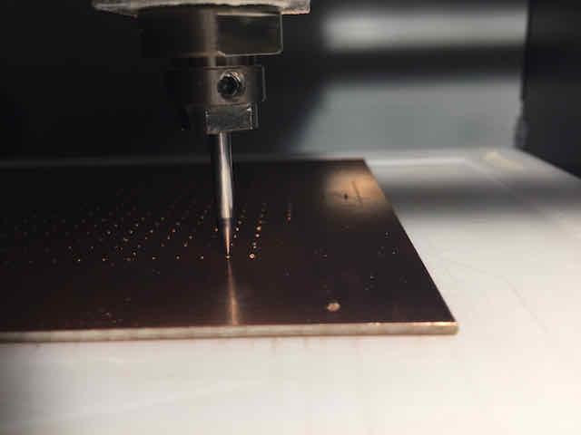
I first used a 0.7mm endmill to mill the via connections, as seen from the top side of the plate. The reason we mill the vias first is that the high amount of friction would place nearby copper traces at risk of beeing destroyed, so we mill these afterwards. We also want to mill the vias first because we will need them to
re-align our board after flipping it over to mill the back-side of it. Although I had previously defined the drill diameter as 0.7mm in my Fusion 360 file, when I set a tool diameter of 0.7mm in Mods, it did not realize the vias. Therefore, I decreased the
tool diameter in Mods down to 0.68mm, which just recognized the vias and resulted in perfect drill holes at the vias locations with the 0.7mmm endmill. Other than that, drilling the vias went without any issues and took about 30 minutes.
Second, I used a 1/64 inch endmill to mill the top traces, as seen from the top side of the plate. Mod's default settings worked without any issue for me, although I adjusted the cut depth to just 0.0005 inch. You can find the settings I used below. This milling run took about 2 hrs.
Next, we have to flip our board over to mill the back-side. I used a few tools to carefully lift and detach the board from the sacrificial ground plate. Although this step can require quite some force, you should not worry too much about bending the FR1 board.
Chances are it is pretty bent anyways after you take it out, and so we want to manually bend it back into shape a bit. Don't worry about too much accuracy here, as we will use double-sided tape again to fix it flat with its top side down onto the bed. I cleaned everythign thorougly with a vacuum cleaner and then
used some double-sided tape on the already-milled top-side. I then mounted the board as parallel as possible to the x-axis again, at the same spot I had it last time. Before we can mill the bottom traces, we still have to define a new origin for our bottom trace cut, relative to where the board with its vias currently is.
Now we see why we milled the vias first: we can now use them to calculate back where the origin of the back-side has to be for the traces to leave out the vias. This calculation is a three-step process:
- Move the endmill around the board by repeatedly adjusting the origin and moving to the origin. We want to move it as closely as possible to one of the vias, within 0.1mm accuracy. For example, the center of my vias was at 87.2mm / 152.3mm – if I move my endmill down by 1mm, it dips straight into the via
- Open your back-side traces image (again) in Photoshop. Enable rulers. Move the origin to the lower-left corner (default is the upper-left corner)
- Create a horizontal and a vertical measuring line which meet right in the center of that via. Measure their values (their distance from the lower-left corner origin) in mm. For example, in my case, they meet at 27.5mm / 10.3mm
- Subtract the Photoshop-measured via offset from the current position of the endmill to get to your file origin. For example, my true origin would be (87.2-27.5=) 59.7mm / (152.3-10.3=) 142mm
- Double-check the origin by moving the endmill to another via by adding the relative offset measured in Photoshop to the origin. You should find that it perfectly goes to all vias you have milled. This is just to make sure you are right.
After we have successfully found and set the endmill origin for our back-side, we can go ahead with milling the back-side.
We flip our board over and apply strong double-sided tape to the top surface after cleaning it thoroughly
To re-align the origin, we move our endmill as precisely as possible to one via as seen from the bottom...

...and then go to the Photoshop file of our bottom traces and calculate back where the origin is, relative to our via
Here, our actual origin on the endmill is the via position -94.2mm in x and -22.3mm in y direction (make sure your Photoshop origin is in the lower left corner)
Next, I inserted a 1/64 inch endmill again to mill the bottom traces, as seen from the bottom side of the plate. I used Mod's default trace milling settings and lowered the cut depth to 0.005 inch, which was enough in my case. The milling took about 1 hrs.
Last, I used a 1/32 inch endmill to mill the outline around the board, as seen from the bottom side of the plate. I used Mod's default outline milling settings. For extra safety, you might want to consider
running your outline script as an airrun first to see if any parts of your board are cut off and if the alignment of your board seems right. Also make sure your board is still safely attached to the sacrificial ground plane.
Using Copper Rivets to Fill the Vias
A via is a small hole in a PCB that allows electrical signals to pass through from one layer of the PCB to another. To get a signal from one layer to the other, they are usually filled with a conductive material, such as copper, and are often plated to improve their conductivity. Although there are through-hole vias (which extend all the way through the PCB) and blind vias (which only extend partially through the PCB), I am only working
with through-hole vias for my double-sided board. When you order a custom board from a board house, your vias will typically be plated and already conductive, so you do not need to worry about plating them yourself. Feel free to skip
to the next section if this is the case for you. As I milled the PCB myself, I had to plate the vias myself. If you think about it, milling a via into a board at this point simply created a hole that extends through the board,
but it cannot conduct any signal (as my FR1 board is only copper-plated on the surface, while the interior is plastic). To get our holes to act as conducting vias, we need to fill them. There are several options for plating DIY vias and making them
conductive:
-
Using solder alone: While this may be your first thought, solder alone is NOT an effective way to plate your vias. Solder is a relatively soft and malleable metal, and it is prone to corrosion and wear over time. As a result,
using solder alone to fill a via may not provide a long-lasting and reliable electrical connection. Also, whenever you fix some component nearby, you might liquify your via solder again and it will simply drip through. Overall, solder alone is not a reliable solution; we need some conductive support material.
-
Using some wire: This is the easiest and fastest way if you only have a few vias and want to avoid the need for any extra material. Simply cut some copper wire (without insulation) and place the wire through the via, with one end on one side of the PCB and the other end on the other side.
Use some pliers to gently bend the ends of the wire over the pads on each side of the PCB. Heat up the soldering iron and apply a small amount of solder to the pads and the wire ends. The wire should now be securely attached to the pads.
Last, trim any excess wire that is protruding from the via using the wire cutters. This will give you a nice conductive via.
-
Using copper rivets: This is a more premium and scalable solution if you need to fill like 250+ vias, as was the case for me. You will also get more reliable connections. Copper rivets are just like any other rivet, but they are tiny and with a diameter slightly smaller than the via hole, so they
fit in and form a conductive bridge between the two sides of the PCB board. To hold them in place and make the connection conductive, we still need to put some solder onto each side of the PCB to the via. Typically, the rivet inner diameter is about 0.25-0.3 mm smaller than the drill diameter, so it can easily be inserted (for instance, I used
0.4mm diameter copper rivets for vias that were drilled with a 0.7mm drill). Make sure to double-check your sizes before you buy your copper rivets.
-
Using conductive paste / plating: This is probably the best but also most expensive solution. You can find vendors that sell specialized conductive paste or plating solutions that you can simply apply to your board in a similar way like
printing solder paste for reflow soldering. These solutions will plate your vias to give you results comparable to those you can expect when you order a PCB from a board house.
As I said earlier, I used copper rivets to fill my vias. Once again, the dimensions you drilled your vias with dictate the diameteter of your copper rivets (obviously). Their shaft has to fit through, but their flat base also has to keep it in place. Best practice, as far as I know, is to
choose a copper rivet 0.25-0.3 mm smaller in inner diameter than the drill you used to drill your vias. I drilled my vias with a 0.7mm endmill, so I chose copper rivets with an inner diameter of 0.4mm / 16 mil, which I ordered from BotFactory.co.
They were also long enough to fit all the way through my FR1 plate. You can read more about the correct choice of copper rivets for your vias in their technical documentation.
To make placing the rivets easier, I put the sides of my board onto two empty FR1 boards, such that the area I wanted to fill with rivets was a few millimeters above the table surface. I also fixed my board and the two supporting boards beneath it to the table with some strips of tape at the sides, such that I could not
accidentally push the board over the edge of my table.
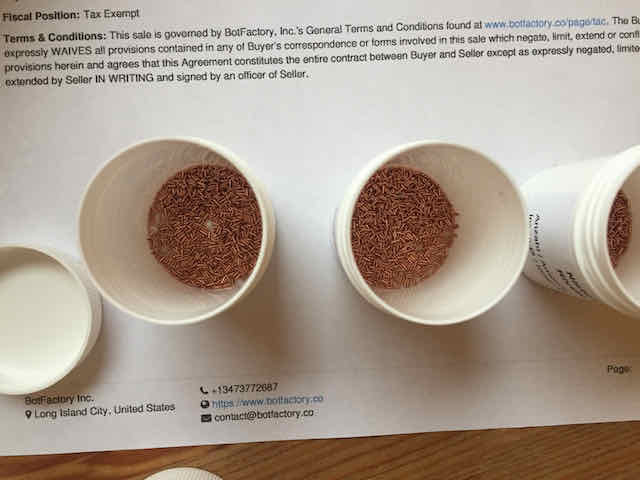
I'm using 0.4mm inner diameter copper rivets – keep in mind there are 1000 rivets in each of these boxes
Setting up my board above two supporting boards and taping everything to the table
Then, I took rivet by rivet and stuck it into the FR1 plate, filling my entire image sensor area one by one. From doing this 256 times, I can recommend holding the rivets with very fine tweezers at their shaft such that their flat head is oriented upwards (oriented correctly). I then used my finger
to make sure their flat head always faced up and was easy to place into the via hole. You will need lots of patience and should take plenty of breaks because you will suffer from back pain. It is incredibly tiring and you will wonder if there is really no better way to doing this, but
as far as I can tell, the time would not be worth the effort of hacking a pick and place machine or something of that sort. It took me about 45 minutes to put down the 256 rivets of my image sensor PCB. Just do it.

The final result
After all the rivets are placed, we want to secure them in place if we move the board somewhere else. As long as they are not fixed to the board, there is nothing preventing them from falling out of your board again, which happens ALL THE TIME by things like shaking your FR1 plate a bit too much, laying it onto a flat surface (remember the
rivets stick out loosely on the other side), or merely breathing onto your plate. I cannot overstate this enough: secure your board and prevent them from falling out whenever you are not actively working on your board. The best way to do this is to get another empty FR1 plate or some other flat material, place it on top of your board, and fix it to your board with some
tape. This traps the flat bases of your rivets and prevents them from falling out. To fix your rivets in their final position, there is an official recommended way and the unofficial way. The recommended way is to get an object shaped like the rivet tool for the specific size of rivet you are using and a hammer. With a supporting board holding your rivets in the riveted PCB
in place, flip your board to the side with the ends of the vias sticking out. For each rivet, place the rivet tool over the copper rivet and use the hammer to flatten the end. This will make the copper rivet stay in place. Later, you use some solder on both sides of the copper rivet to form a conductive connection between the top and the bottom side of your board and the copper rivet.
The unofficial way, which I used, is to simply solder the back side of the rivets straight on, which fixes them in place. Later, you simply solder the other side as well to close the conductive connection between the top and bottom side. While the rivets won't give you flat vias (they will have pointy ends on the back side of your PCB board), it might not matter for your case, so choose whichever you prefer.
Last, we want to test if our connections are conductive as expected. Simply use a multimeter to see if every via connects to the respective column on the other side. I used some tape to stick one electrode to the respective column I was testing, and used the other electrode on the other side of the board going through each pixel in that column.
Overall, you should not find many problems and it will only take you a few minutes. This gives you a perfect double-sided board with filled vias that is ready to be stuffed with components.
Producing a Stencil for the Solder Paste
So far, we have always hand-soldered our components to our PCB board using a soldering iron. Arguably, this is not the best strategy for a board with
256+ components, especially given the regular pattern the pixels are arranged in and their small size. It would be too easy to accidentally short some rows
and columns. To avoid fidgeting around with the soldering iron for hours, we will instead use reflow soldering. Reflow soldering is a process in which a soldered joint is
not created with a soldering iron by hand, but by heating the components and some solder paste to a temperature where the solder liquefies and forms a mechanical and electrical bond
between the components and the printed circuit board (PCB). First, the PCB is prepared by applying a thin layer of solder paste to the pads where the components will be soldered. The paste is a mixture of fine solder particles, flux, and a binding agent.
Then, the components are placed onto the PCB in the correct positions, using a pick and place machine or manual placement. To solder the components, as explained earlier, the PCB is placed into a reflow oven, which uses heating elements to bring the temperature of the PCB and the
components up to the reflow temperature where the solder liquifies, and then cooled down. As you may notice, this is much less hands-on work and much more scalable. It is, therefore, the de-facto standard in manufacturing PCBs industrially.
You may ask yourself how we save much time if we still have to apply the solder paste to each pad individually by hand. In fact, we don't put the paste down by hand. We will use the process of "stencil printing". In general, a stencil is simply a thin piece of material with a pattern or design cut out of it. In the context of reflow soldering, a stencil may be a thin metal piece used to apply a uniform layer of solder paste to the pads on a printed circuit board (PCB).
To use the stencil, it is placed over the PCB and fixed (e.g. using some tape or a mechanical fixture) and a thin layer of solder paste is applied to the top of the stencil. The paste is then pushed through the openings in the stencil and onto the pads on the PCB (e.g. using a credit card to spread the paste).
There are several types of stencils that can be used in reflow soldering, including laser-cut stencils, which are made by cutting the pattern out of a sheet of metal using a laser, and etched stencils, which are made by etching the pattern onto a sheet of metal using an acid or other chemical. Note that when you order a custom
PCB from a board house, you will usually have the option to also order a stencil for your board. In my case, I milled the board myself, so I had to produce the stencil myself manually. Keep reading if you want to learn how to do this yourself; otherwise, skip to the next section.
We first need the pattern of the pads for the stencil. I designed my image sensor PCB in Fusion 360, so I prepared to export the pads as an image export from there. I switched to the PCB tab, hid all layers and then toggled the visibility of just the top layer on. Although my top layer included
all the component footprints I needed, it also contained the routed traces, which we don't want in our stencil. To "hide" them, I used the unroute / ripup function and unrouted all traces (DO NOT SAVE your document afterwards or you will lose your traces – just revert the unrouting after you exported your stencil).
Afterwards, I used the export image command and exported my entire board in monochrome and at 1000 DPI (see Week 3 for my default export settings). This gave me a PNG with just the component footprints I wanted to have solder paste on later. Note that although I am working on a
double-sided board, I will only use solder paste and the stencil for my image sensor side (the top side). Although I only exported the pads, I later realized that I should have also exported the vias, since I needed solder for them as well. Again, make sure you export exactly the footprints that you want to use reflow soldering for later.
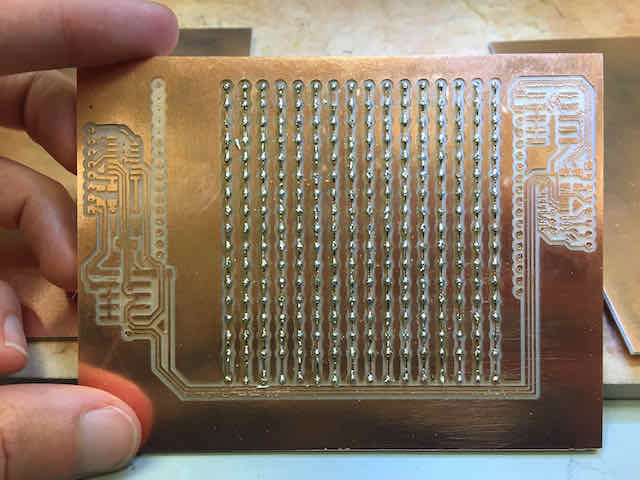
Using Illustrator, I manually re-created a template of footprints and vias to pattern
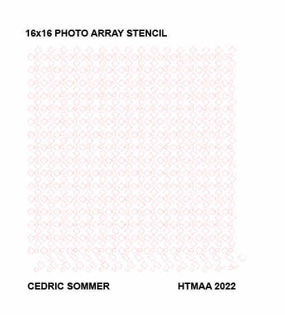
The final template for laser cutting our sencil on a Universal Laser Systems laser cutter
Next, we need to prepare the file for machining the stencil. I chose to laser-cut my stencil, so I had to get it into a vector-based format. You could use a number of PNG to SVG converters for this, like Mods' PNG to SVG program, or load the image into Illustrator and do it manually.
As I only wanted to use my stencil to put down solder paste for the 256 phototransistors of my image sensor and not the other components, I chose to do it manually in Illustrator. I created a new file and adjusted the color settings to RGB and color profile to sRGB. Then, basically, I loaded the PNG into one layer, created the footprint using two rectangles on a second layer, and then simply patterned them across the entire
image sensor area with the offset between each pixel unit. As I am using a Universal Laser Systems laser cutter, I left the fill color blank and the stroke color pure RGB red (#FF0000). Make sure that you are working in RGB mode and that your color profile is compatible with the laser cutter you are using, e.g. using sRGB. Last, I exported
my stencil as a PDF. Make sure there is no re-sizing going on and the footprints are the same size as they physically are when you import them to your machining software later.
Last, the only thing missing is to produce our stencil from our file. A thin sheet of aluminum would be an ideal substrate, but as I did not
have any at hand that day, I instead decided to use some cardstock to produce my stencil. Keep in mind that the thickness of your material will impact the amount of solder paste printed down in that area (the "height" of the solder paste pads, if you will).
The results with cardstock may not be as clean as those you would expect from a
piece of aluminum, and you can only re-use it a few times, but it was perfectly fine for a prototype board like mine. Set your laser cutter up correctly for
the material you are using and then cut it out. For the Universal Laser Systems laser cutter I was using, I printed my PDF and adjusted the settings accordingly for the
piece of cardboard I had. I also double-checked the vector-cut traces had the right color of red (#FF0000) to be recognized. Last, I put in a 15x20 cm piece of pink cardstock
and secured it in the laser cutter using two heavy pieces of metal. One thing to watch out for is where you place your cut job on your substrate. You want to have enough room around your
stencil to secure it in place around all 4 edges, and big enough so that you cover up a decent area around the pads where you might spread solder paste without wanting it. Therefore, I
offset my cut job such that the stencil with an area of 15x10 cm was centered on my 20x15cm piece of cardstock, leaving me with a comfortable margin.
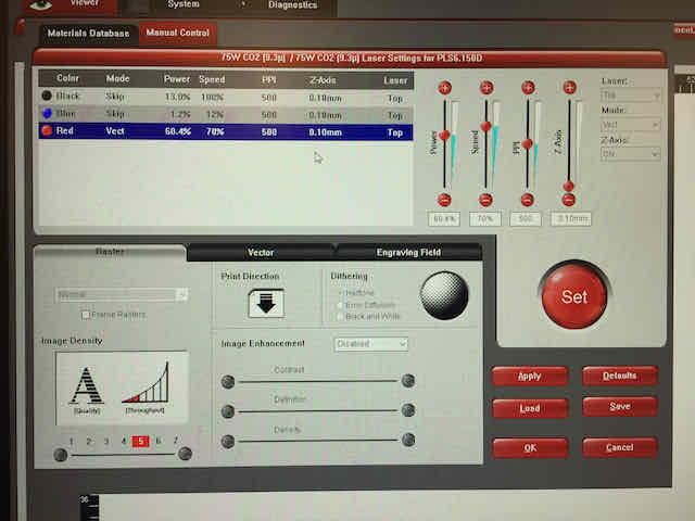
The settings I used on our laser cutter to cut the cardstock
After producing our stencil, we can finally print the solder paste onto the footprints on our PCB board. To do this, we first need to fix the stencil on top of the board in its correct orientation such that
the conductive pads we want to print onto line up perfectly in the stencil. I put two (though you should ideally use four) empty FR1 plates, the same type I used to mill my board, around my board for better grip. I fixed all of them with some
double-sided tape at their bottom. Next, I tried to orient my stencil perfectly so that the phototransistor pads came through where they should. I then used some strong tape to fix the stencil down to the two empty support FR1 plates, holding the
stencil perfectly in place. This might take some time to get right, but it is absolutely crucial since you will apply some pressure to the stencil and don't want it to move.
Last, we apply our solder paste onto the stencil and print it through. I used some generic solder paste we had at our solder stations rated for a reflow temperature of 235°C and put down about 30ml all across the area, which was half of the tube I had.
Make sure you reach the corners and not just the center of the area you want to print, since it can be hard for residue paste to get all the way there. An old credit card or some extra card stock was ideal for me to spread the paste across the entire
image sensor area in long and even strokes, holding the spreaing card at a tight angle over the stencil. Don't worry, the paste will not dry out, and you can also put down more paste if you need to in a certain area. Once you are certain the solder paste is
applied evenly, carefully lift off the stencil from one side. I peeled off the tape on one side and then slowly lifted the stencil up and flapped it over. The result came out perfectly, although I had quite a lot of solder paste on each pad due to the relatively high
thickness of my cardboard stencil (I suppose a thinner piece of cardboard or just some aluminum would have been better). Make sure to wash your hands thoroughly afterwards.
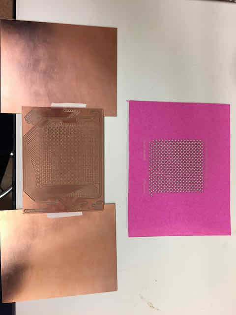
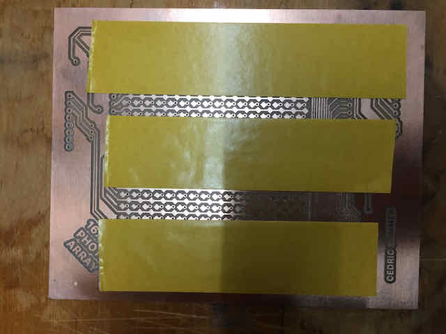
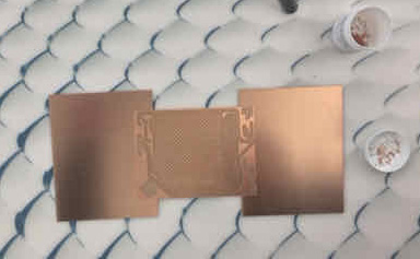
The cut template and the PCB to print on
Stuffing the Board Using Reflow Soldering
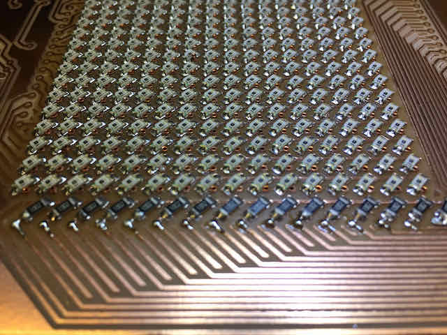
Finally, we can stuff our double-sided image sensor PCB with our components. We previously applied solder paste for reflow soldering to all the 256 phototransistor pads of the top side, so we begin with this side. Ideally, you can use a pick and place
machine for a job like this, but if you don't have one or just want to do it, you can place them manually. My phototransistors came on tapes of 20 or so each, which I opened from one end
component by component. I held the tape in my left hand with the next phototransistor open, while using a pair of tweezers in my right hand to grab the phototransistor and place it in the correct orientation onto my PCB board at the next footprint location with solder paste in place. You will soon see
which way to hold the tape and the pair of tweezers to place your components down with ease. Make sure to press your components feet all the way into the solder paste such that they touch the ground of your PCB board (and not float on top of the solder paste).
It took me about 2 hrs for 256 pixels (I'm rather a perfectionist, so do not expect to take longer than that).
The board, stuffed with all phototransistors and ready for reflow soldering
Next, we need to heat our solder paste to a point where the solder liquifies and forms a soldered joint between our components and the pads. Each solder paste has a unique reflow
solder temperature profile, which dictates the different temperatures and the wait times at each temperature to get the best results for this paste. The different temperatures below the maximum
temperature are for flux and other parts in the solder paste to flow out or evaporate before the solder liquifies and forms a bond. As soon as the solder liquified, the reflow process is over and the heat is usually turned off immediately. There are three ways to achieve reflow soldering:
-
Hot air gun: Arguably the most basic way is to hold a hot air gun a fair distance above your PCB (20cm worked great for me), pointing straight down, and waiting for the solder to liquify. You can even mimic the
reflow soldering temperature profile by putting a thermometer onto the PCB copper plate and adjusting the height you are holding the hot air gun at. If you are lazy, you can also just heat the solder paste straight to its reflow temperature and then remove the hot air gun.
reflow temperature.
-
Sand in pan: A more accurate way is to put a thin layer of sand (max 1cm high) into some pot or pan and heat it over maximum heat on a stove. Place your PCB board on top of the sand and wait for the sand to get hot. Once
the sand and the PCB board reach the reflow temperature, your solder paste will liquify and form the soldered joints we need. This process is great because it is less local and more gradual than the hot air gun, which overall gives you less cold joints.
-
Reflow oven: These devices are specifically designed for reflow soldering (hence, their name) and look like mini ovens. Simply put your PCB board in and program the reflow solder profile
into the software of the oven. Then, run the program to solder your joints. This is the most reliable method, although I usually add a few degrees to each stop to make sure the plate actually reaches the temperature (and not just the oven).
I first used a generic reflow oven/plate in conjunction with a stopwatch to reflow solder the solder paste on my PCB board. The result was clean for most joints, but a few remained half-way liquified. To fix these joints up, I
used a hot air gun locally and ran it quickly across the faulty phototransistors. Overall, this is surprisingly fast.
The photoresistors after reflow soldering. Notice the shiny solder connections
I hand-soldered the vias on the back side to ensure conductivity, but this only took a few minutes
Last, I continued by hand-soldering the remaining components onto my image sensor PCB board using a soldering iron. I have previously listed a few tips for hand-soldering
in Week 3 if you need any advice.
Testing the Board Using a Multimeter
Before we move on to programming our image sensor board, we want to test our joints and make sure all connections are as they should be. I used a multimeter
in my case, but an oscilloscope is also suitable. First, I made sure that no column or row, neither any pin of my other components, was shorted with ground. Next, I
double-checked that no two rows or columns are connected. Last, I checked for each pixel whether it formed the connection it should. I fixed a few cold joints and finished my board.
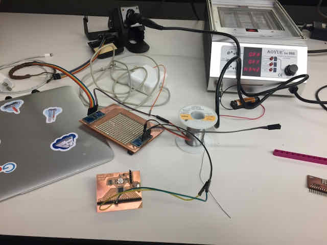
Testing and debugging the image sensor. Note that I connected jumper wires to the multiplexers to test them as well.
Summary
This wraps up this fifth milestone. Today, we have milled an intricate double-sided board and used copper rivets to fill our vias.
We have also learned about the use of a stencil for reflow soldering, and stuffed our image sensor with 256 phototransistors to give it
a final resolution of, well, 256 pixels. Last, we have tested that all connections are soldered correctly. So, the only thing missing is
taking some images with it, right? Almost – we just need to build a motherboard that can connect to the image sensor and read out an image.
In our next milestone, we will finally construct this motherboard and then soon take our first image. If you want to skip ahead and look at the
first images I made, feel free to jump to my last milestone.