Idea
This week, I will be building a 3x3 image sensor that is compatible with the DSLR motherboard I built two weeks ago (see how I build the motherboard).
The idea behind an image sensor is actually quite simple, and this week will drive the simplicity of this concept home I hope. Basically, it is just a 2D array of input sensors that can detect light – for
instance, a photoresistor or a phototransistor. If we arrange a few of these into an array, and light falls onto them, they should all see a slightly different piece of the image. Combined, we would be
able to see an image. Again, one of the best sources of inspiration for this specific part is Sean Hodgin's fantastic 32x32 image sensor (find his detailed protocol on Instructables here).
I was able to adapt and use some of his architecture for my board. However, for a 3x3 array, I wanted to avoid using any external multiplexer processor and instead wire everything up
myself. In this way, this attempt became an interesting multiplexer-from-scratch exercise, and although we would just buy a multiplexer off the shelf today, I nonetheless hope you
can learn something from this with me!
This week is the second part in a series of posts over the coming weeks, which might culminate in a final project. I already created a mother board based on the ARM SAM D21E last week,
with a 2800 mAh LiPo battery last week. This week is all about the image sensor – we will be building a very basic 3x3 sensor as a prototype for a much
larger image sensor later in the semester.
Planning the Architecture of the Input Sensor
This is easily the part where I spent most of my time this week. Finding an optimal circuit was a real challenge, but I am quite happy with my final
design. If you just spend a minute on Google, you can easily find the multiplexer architecture for an LED matrix, where you use row-wise data
lines and column-wise ground lines to turn individual cells in the array on or off. The things people usually turn on or off here are LEDs. The reason this works so
flawlessly is unfortunatey partly built into the system by the fact that an LED is a diode, hence only allows current to flow in one direction. If this weren't the case,
with the typical 2D multiplexer architecture used for LEDs, you could not target individual LEDs because charge could run down other data and ground lines backwards.
While it is not the case with LEDs, this is the case with photoresistors. Therefore, if we turn one data line (row) on and measure one ground line (column), assuning we get the
value at that one resistor, we will instead get the voltage of all the resistors in that column because charge can flow through other connections, being impacted by other resistors, and
finally affect the voltage measured on the ground line. There are several possible solutions around this problem, all with their drawbacks (note, I took inspiration in them from these
two Stackoverflow threads, which were extremely helpful):
-
Solution 1: Put a diode after every photoresistor. While this would solve the issue on the hardware level, I did not like the idea
bcause we ideally want all the surface area of our imaging sensor covered with photoresistors, not anything else that we would sacrifice
resolution for.
-
Solution 2: Set up a system of linear equations that solves for each of the photoresistors values (basically, a 3x3 solver). I did not like this
idea either, because it requires lots of processing power to solve for large matrices, and I want to take my images quickly. So it is impractical.
-
Solution 3: Set up system of linear equations, but this time, only calculate it column-wise. This way, we can calcuulate the value of every single photoresistor
by solving for all the unknown resistors in each column. This solution is the most scalable and reduces computational load (as the complexity of the operation does not
increase exponentially, but linearly). This brilliant solution was mentioned in this Stackoverflow thread.

Working my way through the equations to solve for the resistor values with Leo from my section :)
I eventually settled on Solution 3, because this allowed me to keep the board itself clean of any other components (so I could get to the highest density of pixels), while retaining
a fast processing with my SAM D21E. The design of the schematics for this board is fairly straightforward: I needed three horizontal datalines that I could digitally set to high or low, and
three vertical ground lines that I could read an analog input on. In effect, we then connect a photoresistor at each of the 9 points where the lines cross. Unintended cross-overs will have to be
avoided by adding a second layer to the board, using bridges, or vias. I chose to go with vias and connecting them up with simple copper wires for this first prototype,
creating kind of like a two-sided board, as we only had single-sided boards.
Designing the Schematics
Going with Solution 3, where we solve for the values of the individual photoresistors, I loaded up Eagle (in Fusion 360) and created a new sheet in the existing file of the motherboard I worked on the previous week.
The design rules and libraries were already loaded up in the project, so there was no need to work on these. I first added the connector pins that I forked out of the motherboard to my schematics. This would later make it
easy for me to know which pins I could work with. Afterwards, I added all the other components I needed for my input sensor. You can find the components I used in the list below (all surface-mount):
- 9x Phototransistor
- 3x 10kOhm Resistor
- 3x Jumper Wires
Afterwards, I wired up my schematic according to this template of a similar matrix of analog inputs I found on Stackoverflow.
The schematics are a bit convoluted (it is easy to get connections mixed up while drawing them out), so it is best to work along the
template and double-check the connections every so often. I also had to play around with the ordering of the wires a bit, which is
where the name function was incredibly helpful (as you can simply swap out the names from the pins to the input sensors to change their order).
In total, I used 3 analog input pins and 3 output pins to control my 3x3 input matrix.
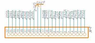
The forked-out pins from my motherboard, which I simply copied to my sensor board
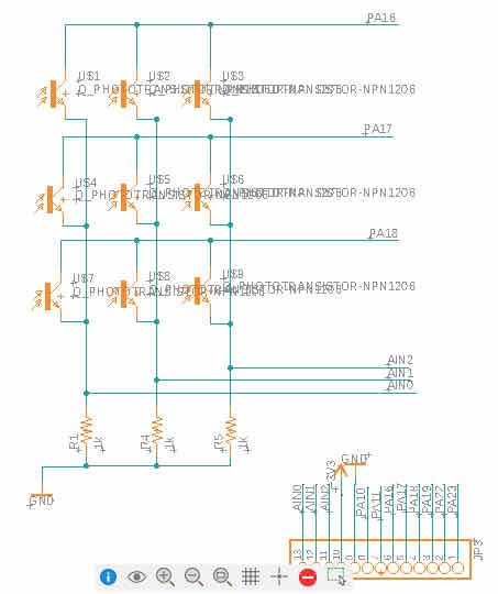
The finished schematics for my input board
Routing the Traces & Finishing my PCB Board
After arranging my motherboard schematic, I switched to Eagle's PCB board tab and continued
by routing the traces of my PCB board. I first struggled to find out which phototransistor in my schematics
corresponded to which on my PCB board, until I realized I could show the names and values of them in the PCB tab
and thus know which one is which. The routing of the traces was quite tricky, as the wires obviously have to form a
grid with lots of overlaps, and only I knew where the vias should go. Also, keep in mind that for a phototransistor,
current will flow from the drain to the source (opposite to what you would expect). I placed the transistors in a 45° angle onto the board
to fit them together as close to each other as possible, and then connected them row-wise on their drains. In a second,
hacky step, I placed a via under each source foot. As the design rules did not allow for this, used a hack to place it there: I placed my mouse
pointer where I wanted to insert a via, and then used the via command in the command line to place a via where my mouse was. Obviously, this is
a hacky workaround and not the way you should do it, so I'm still curious to find out how to place components like vias onto existing footprints.

The final traces for my input sensor array, with the drains connected row-wise and vias placed onto the footprints of the sources
Next, I added the traces for the 10kOhm resistors (with a known resistance value, to normalize the measured transistor charges for our analog inputs).
Wiring them up in the orientation Eagle gave me produced an unnecessarily complex tracing – I found it much easier to wire them up when I
changed some wire names and rotated them 180°. Fixes like these become easier and easier to spot the more you use Eagle. Please,
feel free to check out my list of PCB routing learnings from two weeks ago. Last, I added the outline of my
board and exported my final PCB traces and outline as two separate PNGs. Keep in mind that, in my case, I left the vias on both the traces and outline file to cut them through.
However, most people actually recommend exporting three separate files (traces, vias, outline).
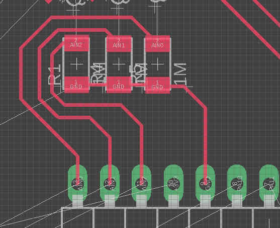
A more complicated routing of the fixed resistors near the bottom of my board

A simpler routing of the same components
Finishing my PCB board by tracing the outline of my board
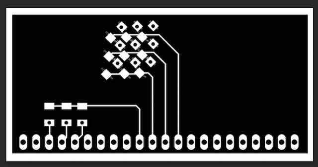
The final export of my traces (with vias) after editing in Photoshop
Milling & Stuffing the Board
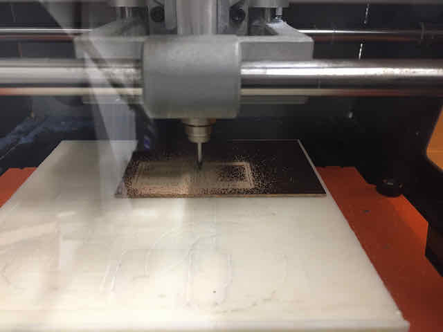
After finishing and exporting both the traces and outline files into a format ready to cut, I went ahead and set up the endmill. The sacrificial ground plate was a bit rough and had a few
bumps, so I decided to use some rough sand paper (120) to sand it down and make it even and smooth again. Next, I put in a new copper plate
in the mill and firmly attached it to the sacrificial ground plate with double-sided tape (see this week on how to do this).
Next, I loaded my final PNG with the traces into Mods,
calculated the toolpaths with the default settings and for a 1/64 inch trace cut, and inserted the 1/64 endmill into the machine. Double-checking the toolpaths revealed
that all traces would be cut in the way I expected, so I went ahead and started milling the traces. Afterwards, I used a 1/32 endmill and calculated the toolpath for an
outline cut in Mods.
Both milling jobs came out very clean, with relatively wide traces and almost no copper splinters. This result was much better than last week, where I used
a ruler and some fine sand paper and still could not get rid of all copper splinters along the edges of my traces. I believe this is because the 1/64 endmill I used
this time was in much better shape, while the one last week might have been overused.
Milling the traces was smooth and at a similar depth all across the board
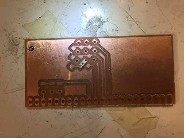
The final result came out very clean
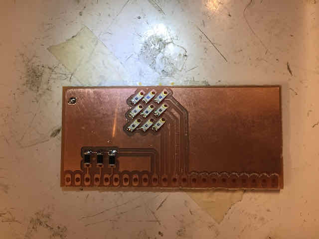
I continued soldering the components of my board, which took me about 2 hrs. I almost went ahead to fast here and soldered on the phototransistors too fast, before I
realized I could use the multimeter to see which direction they should be placed (in my case, the drains should be in the lower-left corners and the sources in the upper-right corners).
Soldering them on the front-side of the board was very easy by putting down some solder on one of the footprints of each transistor, then holding the transistor onto the cold solder with a pair of foreceps,
and then re-heating the solder with the soldering iron. Also, make sure you leave the path for the via clear. After soldering the front-side of the image sensor, I flipped my board over,
and started soldering the column-wise jumper wires. Unfortunately, this was much hackier than I expected (and wanted) it to become. Before you proceed, know that this is NOT the recommended way to do it.
However, as you know, I tend to always take the not-recommended way, so this is another one of these opportunities. Anyhow, for each connection, I fed some wire through to the opposite side of the board without
damaging my lightly-soldered transistors on. I then soldered the respective wire end to the source of the respective transistor. I also used solder on the backside of the board to join the individual wires together to
one continuous wire for each column. Next time, I will for sure do a double-sided board instead of this hack.
Soldering the front side of my PCB board
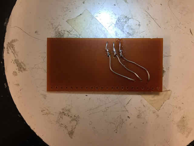
Soldering the back side of my PCB board with jumper wires
Programming & Testing the Image Sensor
My image sensor is designed to be used together with the motherboard I produced two weeks ago. The motherboard already had a bootloader installed and was already programmed with a
simple blink script to blink its on-board LED. I connected the imgae sensor to my motherboard by sliding the 22x1 pins into the respective holes on my motherboard.
Although I did not solder the connections at this point, I was confident that the boards were sufficiently connected for testing and debugging. I hooked up my
motherboard via its micro-USB port to my Macbook again and opened Arduino IDE. Then, I wrote a simple script in C to go through all transistors (according to the logic described in
Solution 3) and output their values from 0-255 via Serial communication on port 9600 in the log. This way, I could test if the sensors all
recorded different values and if my logic worked for decoding the raw light data into an image.
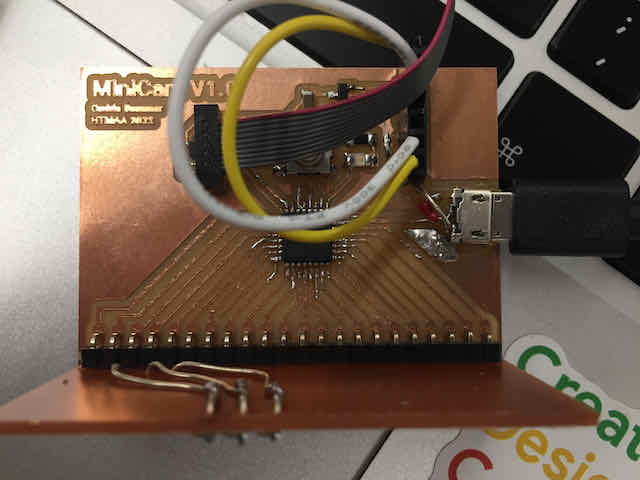
Hooking up my image sensor to the motherboard and programming the motherbard
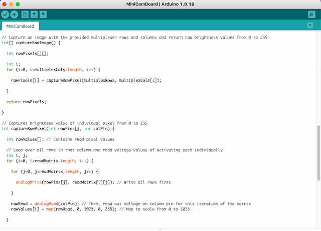
Implementing the logic to read out individual pixels and construct an image for my camera
I tested and refined my script and used a phone flashlight and a laser pointer to test the phototransistors individually. Luckily, they were all soldered on
correctly, and I could read out a valid signal from them. So far, we can only capture an image in an automated way and view it through serial communication to the Arduino IDE.
Next week, I will finally produce a board that allows us to use the camera all by itself – with a small OLED display, buttons to interface the camera, and an SD card slot to
save our images on. This is where it will all come together!

Reading out the analog values of an individual phototransistor

Sequentially reading out all 9 pixels, see Serial output in background (example 1)
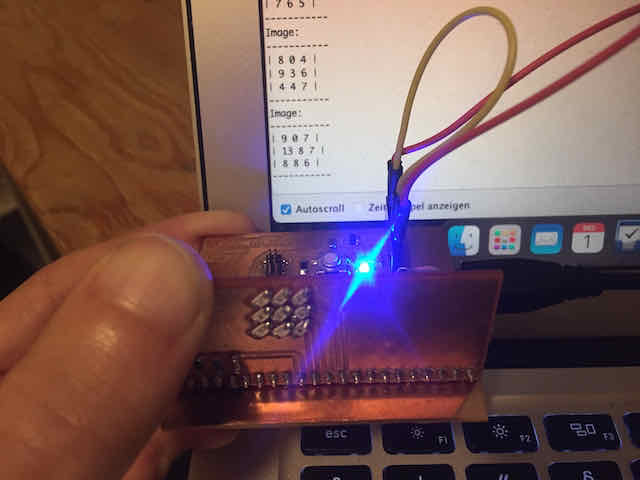
Sequentially reading out all 9 pixels, see Serial output in background (example 2)
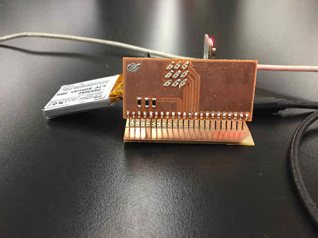
Using the motherboard-image-sensor complex as a "standalone" camera with the LiPo battery!