If you've ever used an SD card to load files onto a 3D printer, you know the pain of running back and forth from the printer to your computer to correct
some problems you only see after the print starts. Wouldn't it be nice to have an SD card you can leave in the 3D printer, and just access over wifi to transfer
files back and forth to it? Well, it turns out there are already wifi SD cards on the market to do exactly that! The only problem is they are expensive, they come with custom
apps you need to install to inteface them, and they are overall hard to work with (at least harder than just natively accessing them from your file explorer). In addition, I
wish I could connect multiple SD cards in a network-like structure, so they all share the same file base (e.g. when I'm out on a photography trip with others and we want to share our files with each other).
This week is a perfect week to fix everything I have ever complained about when it comes to wifi SD cards, because I will build my own from scratch. At the end, we will try to hook up
a network of cards between two SD cards to have them exchange their photos mutually and without any other wifi present.
Architecture of the Wifi SD Card
Compared to last week, this week's board has much less components. I started by listing the features that I wanted to have present on this board in
order to interface any SD slot. One of the most important considerations for me was to make the board as small as possible, so it would not stick too far out
of an SD card slot. I eventually settled on the following features:
Full-size sd card pads (to fit into any SD card slot)
Micro sd card slot (for an actual micro sd card with storage)
ESP-32 (for computing & networking capabilities)
On/off switch
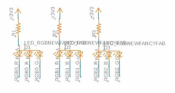
3 RGB LEDs
A key consideration for my routing was the fact that I wanted my board to be as small and slim as possible. This meant that I could
not use the hacky 1.5-sided board designs I have worked with in the past (where I used 0-Ohm resistors as bridges over wires). Instead,
we need a double-sided board to make the routing as efficient as possible and fit as many components as possible into the little space we have.
Let's start by creating the schematics of our circuit.
Creating a Custom SD Card Library
And here we run into the first issue. Unfortunately, the SD Association does not publish the standard for the exact dimensions & sizing of SD cards publicly (they only publish a
simplified version lacking the dimensions you need for free, which you can find here).
This meant that I could not find accurate footprints anywhere online, but had to create them myself. If you want to follow my path, you have two options: You either become a paid member of the SD Association to get the standard with all the dimensions.
Or, you may find this leaked PDF of the standard from 2003 online through Google (I came across this in this wonderful Stackoverflow thread). I'll let you decide which way to go. Anyhow, used the standard as a reference to model the SD card pads to the
required dimensions in Fusion 360.
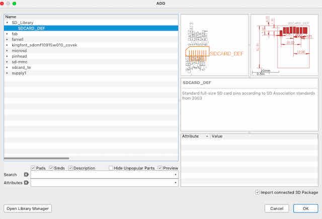
First, I created a new electronics library. I started with the component part (what's on the PCB board), since the dimensions mattered for this
part. Pad after pad, I worked according to the SD card standard to make an accurate replica of the SD card pads. The dimension command was
really helpful here, as a lot of dimensions have to be measured out precisely to get the spacing of the pads just right. Unfortunately, because the
standard is copyrighted and I do not have a license to distribute it, I cannot publish an image that shows the dimensions and how I modeled it. In this regard, you
may just trust that I did so. After creating my new component, I created a corresponding schematic symbol with the
correct pins. Last, I connected the two in order to create a finished component that I could import into my project afterwards. The YouTube video embedded below
greatly helped me understand the process, but it is fairly straightforward if you've designed any board in Eagle before.
Modeling the pads for the standard-sized SD card. The dimensions are accurate, but I cannot show them here for copyright reasons
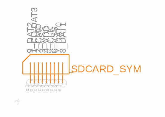
Creating a new schematics symbol for my card
Connecting the pins to finish my component
Designing the Schematics
After finishing my custom library, I started a new electronics project in Eagle (Fusion 360). I imported the fab design rules and the fab library (see this week for how this works). The features I previously defined leave only a small list of components to add to our schematics, which I will
list out below. A lot of the components did not have footprints in the standard fab library, so I had to find custom libraries online for them. I used SnapEDA to find
most of my footprints, which worked like a charm! My only hint is to try to find the library published by the OEM and to double-check the footprints before using them (don't just trust that the author is talking about the same component just because they put the name there).
Here is a list of the components, and links to the custom libraries I used.
1x Full-size SD card pads (created custom library myself – unable to share due to copyright)
Copper rivets (although no true components, I list them because our vias need to match their outer diameter)
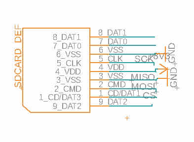
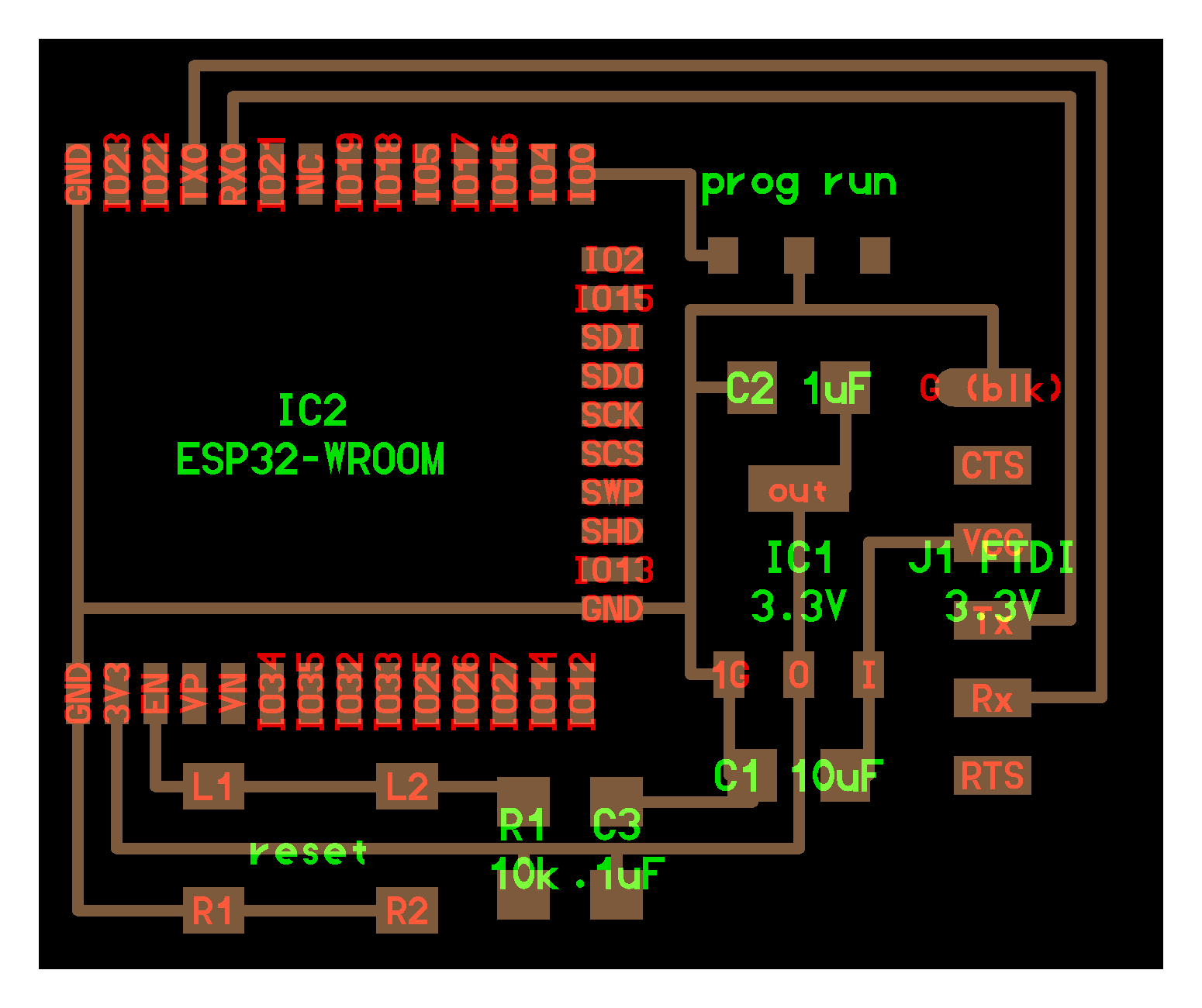
Wiring up this board required much more planning than the previous weeks. This was because I had never used an SD card with a microcontroller before, so I did not know how
SPI worked, nor which pins could run SPI. So, if you're a complete beginner like me, how do you know which pins to use to connect your SD card? The easy answer is
that you might find others who have wired up exactly the same circuit in the past, so you can learn from them. In my case, I was able to find the following
schematic for a wifi SD card by SMDTikhvin on pcbway.com.
Unfortunately, if you think it's as simple as that, you certainly are wrong (at least, I was). The hard answer is that you will have to double-check the schematics to understand what's going on
and what each of the components that user used do, because there is a good chance the schematics you will find online are from people who are just as inexperienced. Digging into my schematics, I found out that
that author was using an ESP-8266, whereas I was using an ESP-32, so the pin mapping does not necessarily work. I also decided I did not need terminal resistors on the SPI lines in my case (read more about what these are here).
Looking into the datasheet (page 27) of the ESP-32 WROOM, and combining the pin information with the Arduini-specific pin mapping given here,
I found out which exact pins were assigned as the default SPI line pins in Arduino, which I decided to use (read below for some more detailed explanation of the SPI protocol). Next came the considerations around the peripherals needed to use my ESP-32. Again, I used the datasheet, but decided that I did not need all the peripherals listed there.
I used HTMAA's ESP-32 basic board (find it here) to understand which peripherals are actually performing which function, and decided to get rid of the 6 FTDI pins to save space.
In my case, I decided to just solder them directly onto the ESP-32 pins while programming my board, and then desolder them once it was working.
My custom SD card pads
Taking note of the datasheet peripheral requirements...
...and then designing it according to the requirements
Adding an on/off switch that drives the EN pin of the ESP-32
After I was confident the SPI lines of both my full-size SD card pads and my micro-SD controller were connected to the SPI pins of my ESP-32, I added some additional
components to extend the functionality of my board. I haven't used RGB-LEDs before as I never had enough pins for these, but I decided to use 3 of them for this project as indicator LEDs to show
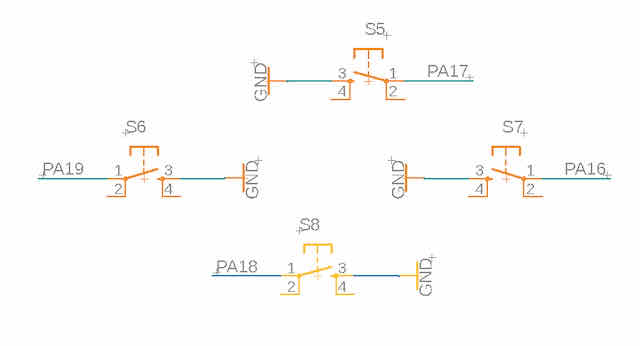
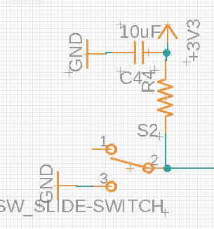
whenever the board is uploading or downloading data. I also added a simple tactile switch as a confirmation button to pair two SD cards. Last, I added a 2-position switch that drives the EN pin, as this
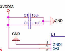
pin has to be connected to 3.3V for the ESP-32 to turn on (so it serves as an excellent on/off switch for the wifi-functionality without harming the SD card itself).
A note about connecting an SD card / the SPI protocol: You might be wondering which pins I used to connect my SD card. To understand the SD card, I
first opened the datasheet of the SSD1306, which you can find here. As any SD card, it uses
the SERCOM (=serial communication) SPI protocol. The protocol requires 4 pins to communicate data: a MOSI pin (=microcontroller output serial input pin), MISO pin (=microcontroller input serial output pin), SCK pin (=serial clock pin) and SS pin (=software-driven serial pin).
Now, when I first read these terms, I did not have any clue as to what this meant and whether or not I could just use any pins from my board. To cut it short: NO, you CANNOT use just any
pins for this. The ESP-32 datasheet lists the pins that can be used for SPI
under the chapter "IO/Multiplexing Considerations". A great and helpful guide to understanding this better can be found here.
If you want to dig deeper and understand the way the signal gets sent, I found this configuration guide to be of great help!
Another video that greatly summarizes it and puts the concept together on a ESP-32-based board is this one by Inventor Andy (embedded below):
Finishing with some status LEDs
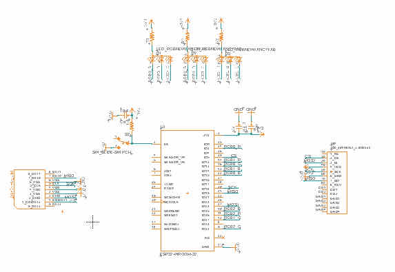
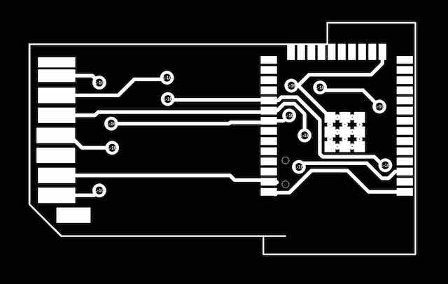
The finished schematics for my wifi SD card board
Routing the Traces of my PCB Board (2-sided with vias)
After arranging my board schematic, I switched to Eagle's PCB board tab and continued by routing the traces of my PCB board.
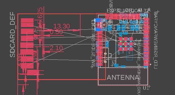
I again started by roughly arranging the components where I physically wanted them to be placed on my final board. One notable difference this week, however, is the
fact that I want my board to be 2-sided. Also, the part of the board that had to fit into an SD slot could not contain any components, so I just offset my components outside that area.
The ESP-32 took up a lot of space on my board, so I decided to keep it as the sole component on one side and use the other side of my board for the micro-SD card slot, the LEDs,
the button and the switch. I used the mirror command to move the respective components over to the bottom layer (layer 16 in Eagle) of my board. After moving and rotating the components for some time, I
ended up with an orientation I liked and decided to go with.
After arranging my parts physially on the board on two sides
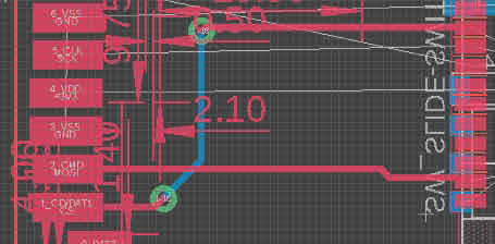
Before I started routing, I set my trace width to 0.4mm (larger than the FAB standard, as I sometimes had trouble milling the 0.25mm traces with worn-out endmills) and my via diameter to 1mm (as this perfectly matched the outer diameter of the
copper rivets I wanted to use). I then started by routing the traces that connect my full-size SD card pads to the micro-SD card slot and the ESP-32. If you have never done this before: to route a trace with a via and continue on the other side,
simply start routing your trace and press the middle mouse button to switch to the other side – or, if you're using a mousepad, while you're actively tracing, type layer 16 into the command line to switch to that layer and
continue your current trace there. Routing the traces on the top and bottom layer was something I had to get used to at first,
but it allowed for much more efficient routes than I could often get on just one side. To save space, I often placed vias right underneath/onto the pads of the ESP-32 or other components, so they did not take up extra space.
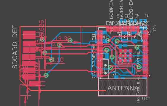
I encountered a few hard spots around the micro-SD slot, which does not allow traces to run all the way underneath it. After the SPI lines and the ESP-32 peripherals were finally routed nice, I continued with the 3 RGB-LEDs. The
order of routing these last really helped me here – although these take 9 pins, they are relatively easy to route (as they provide lots of space to route traces underneath or around them). In short, start with the most "difficult" / inflexible
components and leave the "flexible" ones for the end when you can just put them down anywhere the routing works out.
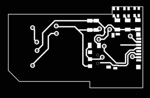
I used vias and a 2-sided setup to do the tracing
The finished PCB board with traces
Some important notes about exporting and preparing files for milling: Exporting and preparing the traces for milling is not a big deal for one-sided boards, but it requires some extra thought for 2-sided boards. It is at this stage where I messed up
the most, so learn from my mistakes (see photos in next section for examples). We have to put some extra thought into the process at three stages: First, in Fusion 360, you want to export the following 4 exports as monocolor PNGs (we will mill them in this order):
1. Top traces: Display the top, pads, vias layers
2. Top vias: Display just vias layer
IMPORTANT: Now, flip the board view in Fusion 360 to see the board face-on from below
3. Bottom traces: Display the bottom, pads, vias layers
4. Outline: Display the dimensions
The final export of my top traces (with vias) after editing in Photoshop
The final export of my bottom traces (with vias) after editing in Photoshop
After exporting your 4 PNGs, we still have to fix them up in Photoshop to be aligned correctly. So second, follow my instructions from Week 5 to create a new Photoshop
document in the dimensions of the 4 exports, then import and embed them all in the document, and cut all layers out with respect to the dimensions of the outline. This should give you a file with
the outline layer nicely visible (upon which you just cut all layers), as well as the bottom traces. The top traces and top vias will likely show nothing, so move these two layers into the cut frame again. Now, to
make sure everything lines up correctly later, we will measure the x-distance between the left-hand border of the canvas (should be x=0) and the left-most via (use helper lines to measure it correctly). Now, switch to the top
traces and vias, and make sure to move both layers such that the right-most via is exactly as far from the right-hand border of the canvas as what you measured before. At this point, you should realize what we are actually doing here:
we are making sure the same via seen from the bottom is where it will actually be if you just flip the board over (note: there are probably other ways of doing this, this is just what I found easiest and most intuitive to understand for me).
Third, after we have made sure our files are aligned, we still need a way to know where to place the origin in milling when we flip the board over. In my case, I placed an extra hole (similar to a via) in the lower right-hand corner of my top via
file. When we later flip the board after milling the top traces, this point will become the lower-left corner on the bottom board, i.e. our origin (note: another possibility would just be to use existing vias and then just move the origin back relative to
where it should be later, but I wanted to be safe). If you want to know what happens if you miss any of these steps, check out my list of fails during milling.
Milling & Stuffing the Board (Failed Attempts 1-3)
This part just describes the different fails I had because of things I missed during the export step, so if you want to know how to do it right, jump ahead to the next section. In my first attempt, I
did not think about flipping the board view in Fusion 360 before exporting my bottom layer. In effect, this meant that I was exporting the bottom traces as seen from the top (through the board) – which means that when you
physically flip the board to mill the bottom of it using the endmill, your traces are mirrored. This isn't a problem for the traces per-se, but your vias will also not line up. So, don't forget to flip your board view in Eagle to top when exporting the
top layers and to bottom when you export the bottom layers.
In my next failed attempt, I forgot to adjust the position of the bottom layers on the canvas in Photoshop such that the vias would be at their exact mirrored positions. As a result, when I milled the top traces of the board, the vias, and then flipped it over to
mill the bottom traces, the vias on the traces did not line up with the already milled vias on the board (as expected, they were shifted in the x-direction). As described above, the fix to this is to make sure the distance from the right-hand side of your canvas to the
right-most via on the top view matches the distance from the left-hand side of your canvas to the left-most via on the bottom view (i.e. the via positions are perfectly mirrored around the center line).
In my last failed attempt, I unfortunately used an 1/64" endmill that was worn down too much at this point, leaving poorly-defined and hairy traces that were not
thick enough and easily came off the board. This is expectable after a few milling jobs, but it still meant I had to use a new endmill and mill out my traces anew.
Milling & Stuffing the Board (How to Succeed)
Routing a 2-sided board is only half the story, as I you probably see from my experiences above. I again decided to use the Roland SRM-20 CNC machine
for cutting my PCB traces. I put a new small copper plate into the machine and attached it to the sacrificial ground plate (which I sanded down a bit) with double-sided tape (see Week 3 on how to do this). The milling itself is
similar to the previous weeks and we will use Mods again to generate our toolpaths. The only thing that changes compared to a one-sided board is that we have more
mill jobs and their order matters:
1. Top traces: Use a 1/64" endmill to mill the traces on the top surface
2. Top vias: Use a 1/32" endmill to mill the vias all the way through (NOT the outline at this stage). Note that one hole should be drilled in the very lower right-hand corner of the file. Also note the orientation of the board, e.g. by using a sharpie to trace the boad outline on the ground plate
IMPORTANT: Now, clean and detach the board from the sacrificial ground plate, flip it, and stick it with the top side down to the ground plate
3. Bottom traces: Use a 1/64" endmill to mill the traces on the bottom surface. Note the origin should be set to be exactly above the little marker hole in the very lower left-hand corner. Also make sure the board is perfectly paralell / has the same orientation as when you milled the top
4. Outline: Finally, use a 1/32" endmill to cut out the outline, as viewed from the bottom side
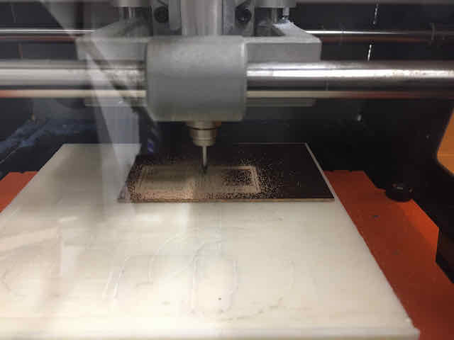
Milling the traces was smooth and at a similar depth all across the board
Place special attention on the part where you flip over and re-set the origin to the marker hole, and everything should be going smooth. I hope my photos help explain the process!
Stuffing the board was relatively easy in comparison. Before we place the components, keep in mind that the vias are simply non-plated thru-holes at this point – nothing is actually conducting a signal through them yet.
There are different ways of solving this (jumper wires, copper rivets, conductive paste, electroplating), and I decided to use copper rivets. The 0.6mm rivets (inner diameter) perfectly fit into the 1mm holes I milled, so I placed one in each hole and
then used solder on both sides of the via to connect the rivets with the copper traces. This gives us a nice 2-sided board with working vias. Stuffing the board with the components is the same process as every week, and I will not go into detail about this part here.
One extra hint: I usually use double-sided tape to secure the bottom of the board on one space while I am soldering the components under the microscope. This obviously does not work as soon as you
have components soldered to one side and flip it over to take care of the other side. However, a bit of clay does the trick as well: just place some down where you usually have your double-sided tape and press the board into it slightly.
Programming & Testing the Wifi SD Card
I hooked up my ESP-32 to my programmer again with the SWD pins, and the micro USB to my Macbook. To get our motherboard ready to be programmed, we first need to install a bootloader.
As a result of my limited understanding of what actually happens in this step, I assumed I could use the same bootloader (for the ARM SAM D11C from the previous weeks and tried to install it with OpenOCD. Unfortunately,
the programming actually worked (that is, it did not throw an exception), so I assumed it worked. This was, of course not the case. Nevertheless, I spent an hour trying to find why the board was not
programmable until I realized this was my mistake. To install the correct bootloader, I went to the Arduino IDE, selected the exact microcontroller I used (ARM SAM D21 E17A) (this was already in my
library that I installed two weeks ago – see here) and hit "burn bootloader".
Per Arduino's console, this worked without issue – and this time, the board was finally recognized on my USB port!
I disconnected my programmer from the motherboard to just use the micro-USB connection, and used the Arduino IDE to write the
simple blink example to it to make the on-board LED blink. I also finally connected the power board with the LiPo battery to the
motherboard, so it could work even when not connected to the USB cord. I also tested the reset button and all I/O pins individually, which worked without issues.
I also tested the serial communication on port 9600, which worked flawlessly. Next week, I will build onto this project and
use some of the forked out I/O pins to connect a custom-built image sensor made from an array of photoresistors. Stay tuned!
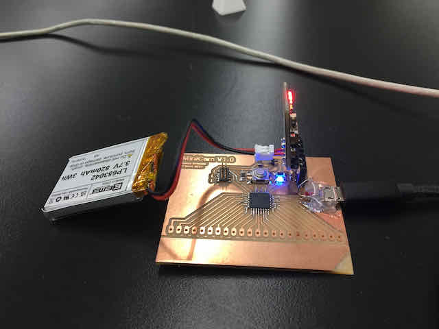
The final programmed motherboard with the power board and a LiPo attached
I had the privilege to be a student in Neil Gershenfeld's MAS.861: How to Make (Almost) Anything in Fall 2022. His class is a digital fabrication masterclass that requires rapid prototyping (and leads to frequent failure). All the projects you can find on this website – as well as this website itself – were built from scratch where feasible. Explore other projects or take the class yourself from any maker space around the world through FabAcademy.