(Text to be updated)
Idea
This week is an extra add-on for the simple DSLR camera I started two weeks ago. So far, the camera
has a motherboard with a LiPo battery attached. It also has a simple 3x3 image sensor of phototransistors to record an image, and an OLED screen
and menu buttons to interface it. By far, the number one feature still missing is to be able to export my images to a computer and look at them there.
However, I also would like to be able to see them on a smartphone. I have always wanted to buy one of these wifi SD cards, but they were always outside my
budget and I did not like most apps and webapps that came with them. This week is a perfect week to build my own and I hope I will be able to finally capture and look at some images by
the end of this week on my smartphone or in a webbrowser.
This week is the fourth part in a series of posts over the past weeks. I created a motherboard based on the ARM SAM D21E two weeks ago,
with a 2800 mAh LiPo battery. Last week, I created a simple 3x3 image sensor to actually capture an image and an interface (OLED screen and menu buttons)
to access the camera.
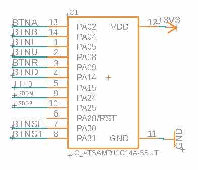
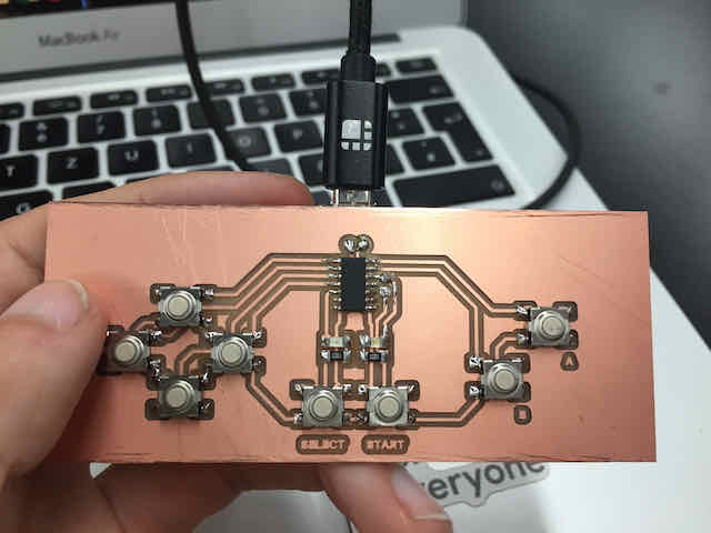
Architecture of the NES Controller
Compared to last week, this week's board has a much simpler architecture. I started by listing the features that I wanted to have present on this board in
order to interface the camera. Although I probably had 1000+ wishes for things for my camera to have, I eventually settled on the following
features and their respective components. This is the most straightforward approach from my point of view, since adding those components to our
schematics will be the first step once we switch over to Eagle for the design of our PCB board. The features are listed below, the
respective components are listed in the next part.
- Full-size sd card pads (to fit into any SD card slot)
- Micro sd card slot (for an actual micro sd card with storage)
- ESP-32 (for computing & networking capabilities)
- On/off switch
- 3 RGB LEDs
I did not do much planning for the tracing, but figured that most should be rather easy to trace once I have my schematics
live. Therefore, I jumped straight into the schematics in Eagle.
A quick sketch of my wifi sd card board and the integration into the output board
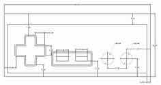
A quick sketch of my wifi sd card board and the integration into the output board
Designing the Schematics
Since this board should be able to connect to the breakout pins of my motherboar (the same ones that the input board gets), I
started by opening that Eagle electronics project from two weeks ago. I did not want to mess up the old schematiccs, so I instead
created a new sheet. First, I copied the pin head over from my motherboard, mirrored it (because I wanted the output board to be connected in
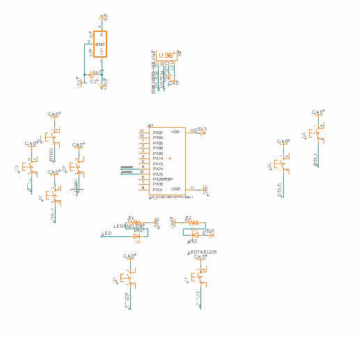
the inverse orientation), and added it. Then, I added the following components to my schematics:
- 1x ESP-32
- 1x Full-size sd card pads
- 1x Micro sd card adaptor
- 1x 2-position slide switch
- 2x Capacitors
- 3x RGB LEDs
In total, I only had 7 digital pins to spare for my output board. This meant that I had to come up with a smarter way
of wiring my components than just giving all components their own pin. Furthermore, I remembered that the imaging sensor board
(which is connected to the same pins, just in the opposite direction) used 3 digital pins on its own when capturing an image. I
figured that I could re-use these pins for the take photo tactile button and the slide switch to switch between image capture and
image review mode, as long as I was ok with the fact that while the camera takes an image, these buttons could be used. This
sacrifice was acceptable for me (in fact, most DSLRs also don't allow you to do anything while an image is being captured).
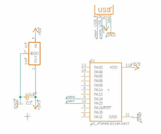
I then used 4 of my 7 remaining pins for my 4 menu buttons and 1 pin for the red status LED, which left me with 2 more digital pins for the
OLED screen.
My custom SD card pads
Taking note of the datasheet peripheral requirements...
...and then designing it according to the requirements
Adding an on/off switch that drives the EN pin of the ESP-32
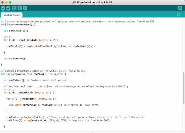
A note about connecting an SD card / the SPI protocol: You might be wondering which pins I used to connect my SD card. To understand the SD card, I
first opened the datasheet of the SSD1306, which you can find here. As any SD card, it uses
the SERCOM (=serial communication) SPI protocol. The protocol requires 4 pins to communicate data: a MOSI pin (=microcontroller output serial input pin), MISO pin (=microcontroller input serial output pin), SCK pin (=serial clock pin) and SS pin (=software-driven serial pin).
Now, when I first read these terms, I did not have any clue as to what this meant and whether or not I could just use any pins from my board. To cut it short: NO, you CANNOT use just any
pins for this. The ESP-32 datasheet lists the pins that can be used for SPI
under the chapter "IO/Multiplexing Considerations". A great and helpful guide to understanding this better can be found here.
If you want to dig deeper and understand the way the signal gets sent, I found this configuration guide to be of great help!
Another video that greatly summarizes it and puts the concept together on a ESP-32-based board is this one by Inventor Andy (embedded below):
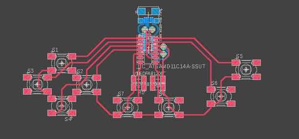
Routing the Traces & Finishing my PCB Board (2-sided)
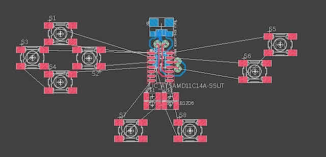
After arranging my board schematic, I switched to Eagle's PCB board tab and continued
by routing the traces of my PCB board. Again, roughly arranging the isolated parts of my board as I
did in my schematics helped me get to a possible physical layout quickly. I highly recommend this as a quick way
to get to an initial design that you can start working on. Although I first had some airwires
overlapping each other in my initial design, I could resolve all of these issues by changing the names of the pin wires my components were
wired to. You'll see some of the choices I made to make my routing as easy as possible in the screenshots below.
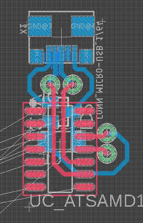
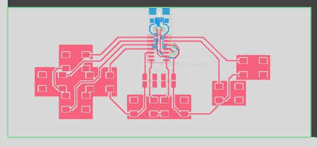
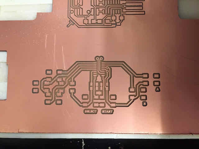
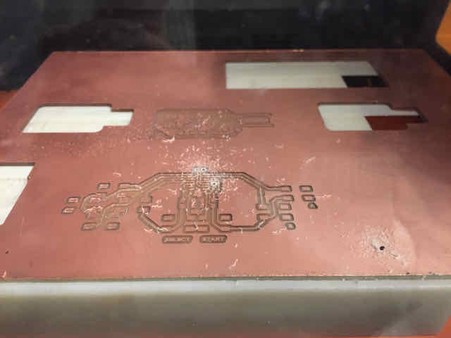
I used vias and a 2-sided setup to do the tracing
The finished PCB board with traces
After I had all my components routed in an efficient way, I added the outline of my
board. Although I did not nearly need as much space as I used in the end, I gave my output board the same dimensions as the input board I prepared last week by
copying the outline of that board. This is to make it easier to glue the two boards back to back. I then exported my final PCB traces and outline as two separate PNGs.
Again, I left the vias on both the traces and outline file to cut them through in my case. However, most people actually recommend exporting three separate files (traces, vias, outline).
I used vias and a 2-sided setup to do the tracing
The finished PCB board with traces
Milling & Stuffing the Board
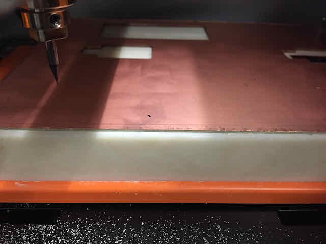
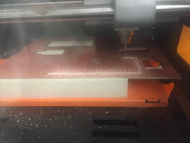
After finishing and exporting both the traces and outline files into a format ready to cut, I went ahead and set up the endmill. I decided to use the Roland SRM-20 CNC machine
for cutting my PCB traces. I put a new copper plate
in the machine and firmly attached it to the sacrificial ground plate with double-sided tape (see this week on how to do this).
Next, I loaded my final PNG with the traces into Mods,
calculated the toolpaths with the default settings and for a 1/64 inch trace cut, and inserted the 1/64 endmill into the machine. All toolpaths looked well separated,
so I went ahead and started milling the traces. Afterwards, I used a 1/32 endmill and calculated the toolpath for an outline cut in Mods, which I subsequently cut.
Both milling jobs came out perfectly clean, with relatively wide traces and almost no copper splinters. I just quickly
washed the board under tab water with dish soap, let it dry, and felt ready to proceed to stuffing.
I used vias and a 2-sided setup to do the tracing
The finished PCB board with traces
The finished PCB board with traces
The finished PCB board with traces
The finished PCB board with traces
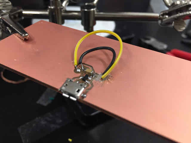
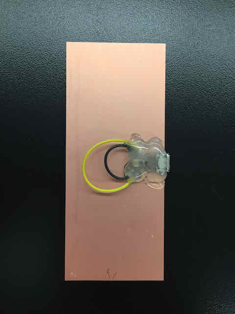
I continued by soldering the components of my board, which took me about 30 mins (not a big deal with the few components I had). I only permanently mounted the buttons and the LED; the
SD card was attached just by soldering on some pin-heads onto the board. I highly recommend using pin-heads for whole isolated component boards like these (I have to remind myself about that).
I used vias and a 2-sided setup to do the tracing
The finished PCB board with traces
The finished PCB board with traces