Idea
After learning the basics about prototyping PCB boards and doing a hello world board two weeks ago, I felt
like I wanted to start making something more complicated and useful. This week is the first part in a series that
I will spread out over the next three weeks or so. As a photography (or, shall I say, imaging) enthusiast, I am
fascinated by the optics and electronics in modern-day cameras. After watching the YouTube recordings of Harvard's DGMD E-10: Exposing Digital Photography
by Dan Armendariz course this winter, I got into the idea of building one from scratch. Another point of inspiration
was Sean Hodgins fantastic 32x32 image sensor (find his detailed protocol on Instructables here).
His monochrome 32x32 image sensor really layed the groundwork for my attempt, and I would love to build onto it and replicate some more
of the features we find in modern-day DSLR cameras. Specifically, I hope to build a DSLR with RGB capabilities, analog ISO, a faster processor,
as well as motorized functional components like a mirror, shutter, and aperture. Maybe even capabilities for flash photography. Let's see how far we can get!
This week will be the first part in a series of posts over the coming weeks. I will start by designing the electronics first, and then build
the housing afterwards (since its dimensions are largely driven by the size of the electronics inside). This week, I will create
a motherboard for my DSLR camera. It is rather simple and should house the main microcontroller (an ARM SAM D21E so far, although I will likely switch to a larger controller later)
and adapters to all necessary peripherals (micro USB, power supply, pins for image sensor, pins for user interface/buttons).
Planning the motherboard
Looking back, I feel like I spent most of my time this week on the drawing board. Although I felt like the motherboard would be rather
simple to design, I quickly realized that I needed to know all peripherals I wanted to add later in advance, in order to choose
a microcontroller with the right capabilities and pins. On the other hand, we did not even have the controllers available that I needed for
the more complex capabilities I envisioned. In the end, I decided to go with the ARM SAM D21 E for a first prototype. Although the controller is
still quite limited with regards to its number of programmable i/o pins, it was the largest we had and I felt confident about finding ways
to use the same pins for multiple purposes. Also, using a small chip helps scope the project down to a manageable prototype first, before
going all the way to a much bigger processor for a final project. One big learning here is that all the time planning a project like this intensively
will greatly pay off later, when you can do the schematics in one simple go, rather than changing components over and over because they aren't right. Another
learning I take from this is that if it takes you too much time to plan for all circumstances (and it's not a NASA mission), it likely means the project has
become too complex for how much you know about it and prototyping a scaled-down version is the right way to go.
Designing the Schematics
I worked in Eagle (in Fusion 360) to design the schematics and PCB layout of my motherboard. First things first, I created a new
project, created an empty schematic and synchronized PCB layout, and loaded the design rules. I chose our fab lab's design rules (the same I used in my first PCB board).
The whole design rule checking process saved me a ton of debugging last time, so there was no point in not getting the basics right. Next, I loaded
the part libraries I wanted to use for this project (in my case, our fab lab's library, as well as the supply and pinhead libraries).
Setting the design rules before any work happens
First, I added all the components I wanted to use on my motherboard to the default schematics sheet of my project. The complete parts list can be found
in the project file below or here (all surface-mount, unless stated otherwise):
- ARM SAMD 21 E17 // microprocessor
- 5x2 pinhead // SWD for SAMD
- 3.3V 100mA regulator // to regulate voltage from power source down
- 10µF capacitor // for regulator to prevent voltage spikes
- Female micro-USB header // for USB connection
- Tactile button // as RESET button
- 10kO resistor // pull-up resistor for RESET button
- Blue LED // as status led
- 500O resistor // as resistor for status led
- 6x1 pinhead (thru-hole) // connecting pins to power supply (to be added later)
- 22x1 pinhead (thru-hole) // connecting pins to I/O board (to be added later)
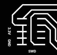
I then started wiring up the schematics using the datasheet provided by ARM, particularly the pinout diagram on page 26 for SAMD21E controllers.
Connecting the 5x2 SWD pinhead, the regulator, capacitor, as well as the RESET and status led logic was quite easy, as I had
used the same components two weeks ago for a SAMD11. For these components, I felt confident in the way they were
hooked up. I had not used a micro-USB header before, so I quickly read up the documentation about how the lines are connected.
Last, I added the 6x1 and the 22x1 pinheads to connect a power supply and an I/O board later. The 6x1 pinhead was directly wired
with consideration of using a 3.7V LiPo battery and the micro-USB header to charge it. It is important to note that LiPo batteries should
never be hooked up directly to the circuit, but always have a charging circuit that takes care of power management (including parallel charging,
safe discharging, and reading the charge level). Luckily, there are tons of ready-made PCB charging boards out there that take care of just that.
The 22x1 pinhead was chosen rather arbitrarily – it simply connects all programmable i/o pins of the SAMD21E, which can be used in a connecting board later. To be honest, I did not
finalize my thoughts about how many pins I would need, so I simply forked out all of them and will later decide about their usage. In hindsight, this
was quite smart, as the pins did not hav any other useful function once I completed the motherboard, so I might as well just pass them down to the next board.

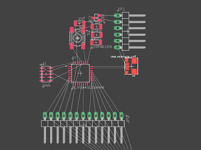
The heart of our motherboard: a SAMD21E
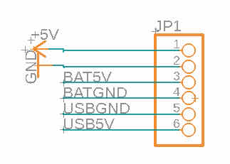
The 6x1 pinhead for the power supply board
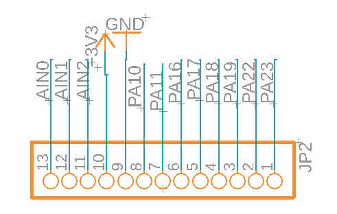
The 22x1 pinhead for all I/O pins

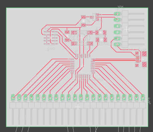
The final schematics
Routing the Traces & Finishing my PCB Board
After arranging my motherboard schematic, I switched to Eagle's PCB board tab and continued
by routing the traces of my PCB board. This was the first time I was starting the routing from scratch and without a template,
and I first struggled to find a good starting point. Eventually, I started with the microprocessor and started arranging the components with the most
connections to it around it, so they would not overlap. In general, I prioritized the pin connections over routing the voltage and ground lines, since I felt like
I could just trace them around the edge of the board later. Although this did not always work, it got the job startd. I made a few more learnings on my way which I will probably refine over the next
weeks, but maybe they help you, too:
- Start with the "main component" with the most connections and then work your way down
- Arrange the components in sections / regions first, so interconnected components are near each other (e.g. regulator and capacitor). Worry about rotations later
- After that, play around with rotating the individual components
- Wire the pin connections first. Worry about voltage and ground later (they are almost everywher across the board)
- Large components have lots of space under them for traces through them (including connecting voltage and ground pins on opposite sides of a microcontroller)
- Buttons, LEDs, resistors, etc. are great bridges across wires
- It's ok to break design rules for a smart hack (usually a connection under something)
Starting the layout of my PCB board
As we use an endmill and one-sided boards in our fab lab, I used a couple of hacks to get to a board design that did not need any vias or bridges. Although jumper wires
or 0O resistors could be used for this purpose, I really wanted to avoid using them. In the end, I was able to get a board that didn't need any more components.
Some of the hacks I used to get to this design can be found in the images below.

Routing the main ground and 3.3v lines under the tactile reset switch
The finished board layout with outline
After finishing my PCB design, I exported the traces and the outline as monochrome PNG images and started cleaning up the design in Photoshop. I created a new document with the same
dimensions as the raw exported images and then embedded both the traces and outline PNG in the working file. I cropped both images down to around the
outline of the board, added a white (non-cut) margin around the board, and added text labels with the name and version of the board. Here I discovered one of the hackiest but best
learnings this week: I could easily fix up small mistakes or issues in the design in the PNG directly (as long as I felt confident about how the
machine paths would be traced around them). I used this to remove some larger footprints to leave more space to some traces.

The final traces in Photoshop (with text)

The final outline in Photoshop (with holes)
I added in some explanatory text for the wiring and also cleared the footprints for the trace under the 5x2 connector

Fixing the space between the outermost traces, as the steep angle creates a gap too narrow for the endmill to cut
Milling & Stuffing the Board
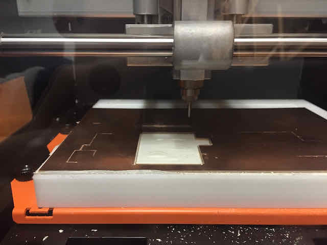
After finishing and exporting both image files into a format ready to cut, I went ahead and set up the endmill. An existing one-sided copper-plated plate was already
in the mill and firmly attached to the sacrificial ground plate with double-sided tape (see this week on how to do this), so I went
ahead with it. I played around with the position of the drill until I got it positioned right next to a previously cut board. I then loaded my final PNG with the traces into Mods,
calculated the toolpaths with the default settings and for a 1/64 inch trace cut, and inserted the 1/64 endmill into the machine. One important thing I learned two weeks ago is
to never trust my design file, so I double-checked the toolpaths preview and looked for anything unexpected. I quickly realized that two of the outermost I/O pins on my board
had very steep angles, putting the traces so near to each other that the mill would not cut a separation between them. Though not ideal, I used Photoshop for the moment to pull the
traces apart from each other.
When I finally started milling the traces, I realized the 1/64 endmill did not cut the traces properly – it barely scratched the copper surface. Clearly, it was too high. After double-checking
all settings, I doubled the cut depth from 0.004 in to 0.008 in and started the job again. This time, the endmill cut the material perfectly. I also noticed the material on one side of the board being cut
more generously than on the other side – a typical sign for an uneven board. As a matter of fact, I was able to see the
slight curvature in the surface of the board, but could not figure out a way to make it flatter. I went with the results this time, but ideally, a new
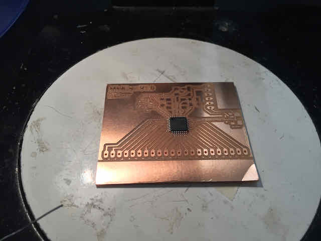
board shouild be attached to fix the problem. After the traces, I cut out the board outline and the holes, which went smoothly. All in all, the
milling took about 1 hr of time – much more, than I would have expected. The final result still had lots of copper splitters, so I scratched the surface of the
board with a metal ruler a few times and then washed it under cold water.
During the first attempt, the endmill was not deep enough, not cutting the traces properly and evenly
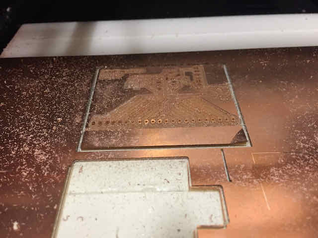
The end result after increasing the cut depth has clear traces, although some are still joined together and have to be separated manually later
I continued soldering the components of my board, took me about 1 hr. By far, the most challenging part was soldering the microcontroller with its numerous pins and the
tiny gaps between them. However, I found two hacks that did the trick for me. First, when I could not get accurate results, I put down solder on and across all pins of the microcontroller
and then used a piece of copper braid to "reduce" the free solder in between the pins. This cleared the gaps between them while leaving solder on the pins themselves. Second, after
a few rounds, I was able to consistently solder the pins on one by one. It is very helpful to keep the heat conductance in mind for this: by heating both the pin and the copper
under it for some time, and then exposing the connected copper trace to some solder, I could usually get the solder to "flow up" the trace to the pin, connecting the two. Another challenge
was the micro-USB port – not so much because of its size, but because the endmill did not separate the traces well enough. I just used an exactor knife to cut
a channel between the connected wires and then soldered the connector on. All other components went with ease.
By far the most challenging part during soldering was the SAMD21E
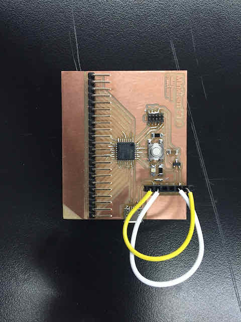
The finished stuffed board with all components soldered on. Note that I used jumper wires to directly connect the +5V and GND lines from the micro USB port to the regulator, as I did not have my power board attached yet.
Programming & Testing the Board (Not Yet)
Because I did not have a power board and battery yet, I used jumper wires on my power board pins that bridged the +5V and GND lines from my micro USB port directly to the 3.3V regulator. Later, I removed these and put the PCB charge board in its place that
uses the USB power to control the charging of the LiPo battery, while controlling the discharging into the circuit separately. I used my programmer from week 3 to program my motherboard.
I connected the target pins of my programmer to the SWD pins of my motherboard and the micro USB to my USB port. Unfortunately, I did not realize the micro USB port was structurally extremely weak on the board, so when I tried pulling the USB cable from it,
I accidentally ripped the port off the board. Even worse, I ripped off the entire power line! Oh boy, this would need some serious surgery. And yes, while I agree it would have been much better at this point to just mill a new board, I thought I could probably get this
surgery done in less time...I returned to the soldering station and soldered on jumper wires for the +5V and the GND lines from the USB port to the power supply board. After making sure I did not short them, I used hot glue to glue the entire structure in place as it was.
Again, not something I can recommend, but I was greedy and really wanted to test my board.
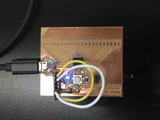
Ready for programming...
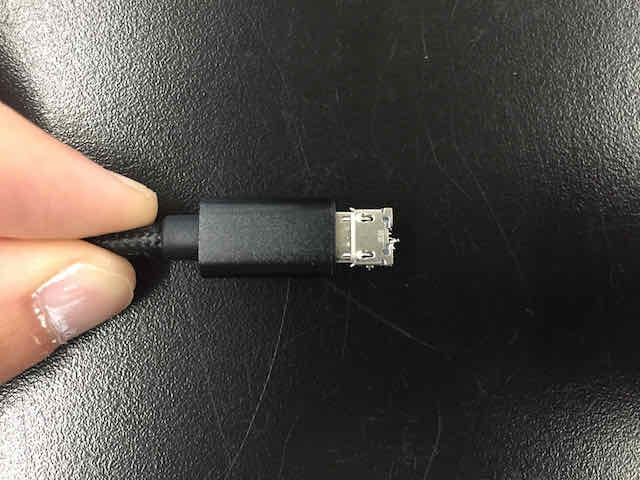
...until this happened
Programming & Testing the Board (For Real)
I hooked up my motherboard to my programmer again with the SWD pins, and the micro USB to my Macbook. To get our motherboard ready to be programmed, we first need to install a bootloader.
As a result of my limited understanding of what actually happens in this step, I assumed I could use the same bootloader (for the ARM SAM D11C from the previous weeks and tried to install it with OpenOCD. Unfortunately,
the programming actually worked (that is, it did not throw an exception), so I assumed it worked. This was, of course not the case. Nevertheless, I spent an hour trying to find why the board was not
programmable until I realized this was my mistake. To install the correct bootloader, I went to the Arduino IDE, selected the exact microcontroller I used (ARM SAM D21 E17A) (this was already in my
library that I installed two weeks ago – see here) and hit "burn bootloader".
Per Arduino's console, this worked without issue – and this time, the board was finally recognized on my USB port!

I was lazy and first tried installing the SAM D11C bootloader from last week, which did not throw an exception but did not give me a programmable board (as mine was a SAM D21E)
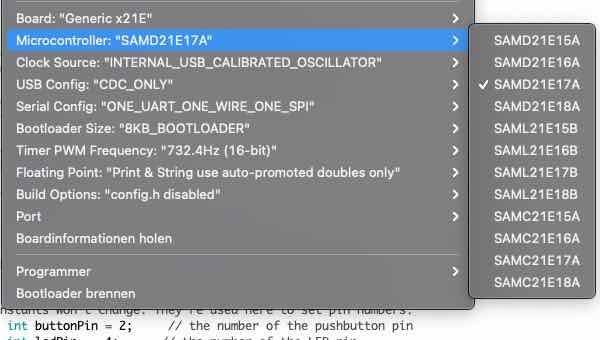
You can also use the Arduino IDE to burn the bootloader for your board. I chose my board from this dropdown menu...
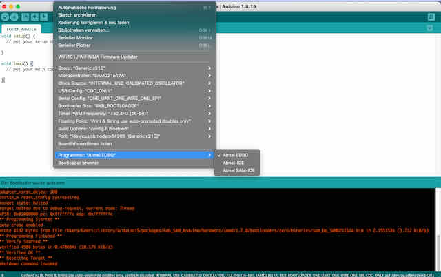
...and then selected the EDBG ICE implementation to burn the bootloader to my board. Keep in mind that this requires your programmer to be connected to your machine – not just your unprogrammed processor (as this one cannot be identified by your machine just yet)
I disconnected my programmer from the motherboard to just use the micro-USB connection, and used the Arduino IDE to write the
simple blink example to it to make the on-board LED blink. I also finally connected the power board with the LiPo battery to the
motherboard, so it could work even when not connected to the USB cord. I also tested the reset button and all I/O pins individually, which worked without issues.
I also tested the serial communication on port 9600, which worked flawlessly. Next week, I will build onto this project and
use some of the forked out I/O pins to connect a custom-built image sensor made from an array of photoresistors. Stay tuned!
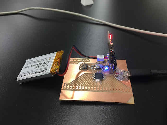
The final programmed motherboard with the power board and a LiPo attached