Assignments
The individual assignments for this week are:
- use an EDA tool to design a development board to interact and communicate with an embedded microcontroller
Designing a board
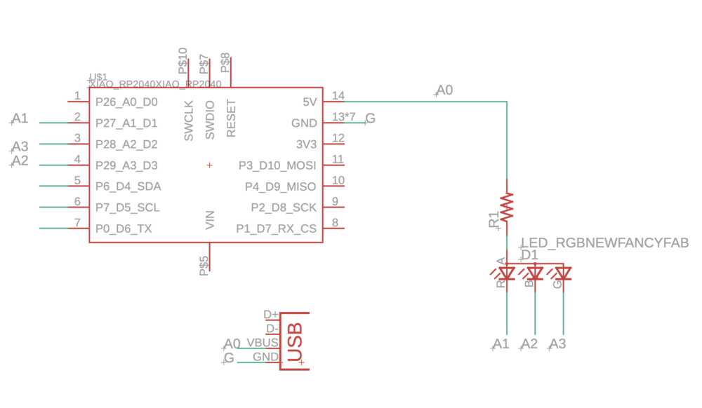
The Schematic
Since I have no prior experience in designing PCB’s and it was recommended in class, I decided to use Eagle in Fusion 360 for my PCB design.
Since I’m still undecided on my final project, and hence I’m not sure what I want the board to be able to do, I decided to just have the board have a few pins broken out, and have a simple feature.
Thus, I decided to have the board connect to a RGB LED, as well as have an USB A connector broken out.
The schematic looked like this
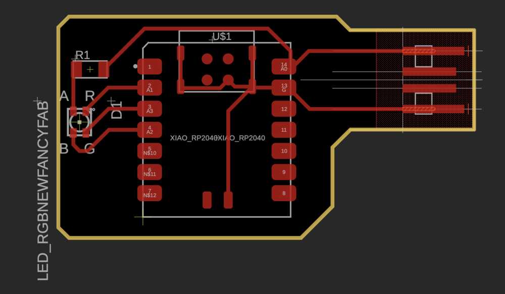
The PCB
The board had a simple design where three pins were broken out to control each of the RGB color channels in the LED. I connected each of the pins to their respective pin on the LED.
I used the trace sizes recommended in class on the board, and only ran into a few issues with how close the traces were, which I fixed quickly by moving them around.
The final step was to draw a box around the entire thing, which would be the outline of the PCB. I chose to add bevels to the corners so that they wouldn’t catch as easily on clothing/poke when handling.
And the final PCB looked like this
Later board design
For my final project, I designed a different PCB that had three Xiao ESP32S3 Sense boards on it. The key requirements for this design were that the three boards would communicate with each other using I2C which was built into the PCB, breaking out the I2C lines for communication with another device on a different board, and all of the remaning analog/touch pins being broken out for detecting multiple holds. I also had each board have an additional non analog GPIO pin be broken out, for use as a digital line if I needed it.
More details can be found at the top of Networking and Communication Week