Having been introduced to embedded microcontroller systems for the first time in Week 3 (embedded programming), my only experience with these devices was in soldering and programming one. This gave me some familiarity to the components that may be involved and their basic functionality, but I am still very much a beginner to all things electrical-- as Anthony, who kindly explained the functionality of pins to me about four times in one day, could attest.
In our introductory discussion to embedded microcontroller systems, we reviewed the Autodesk Fusion (FKA Eagle) workflow for designing boards. I was pleased to learn of this tool integration because Fusion has quickly become my preferred environment for mechanical design, CAD, and now electronics. To get acquainted with the basics, I watched the Fusion section of this Recitation from 2023 and reviewed this demo about schematic design in Eagle.
From an interface point of view, one of the biggest challenges to me this week was wrapping my head around the fact that different representations of microcontrollers will show different information about the same physical component. This is a factor in the Fusion enviroment which shows the
Schematic
(diagrammatic outline of a board; components are not spatially connected but logically linked by labels) and
PCB
(components are spatially connected, not labeled; you have to draw the tracks to confirm connections) expressions of the board separately. For me, this complexity was most apparent in the differences among these represntations and the actual pinout of the microcontroller component.
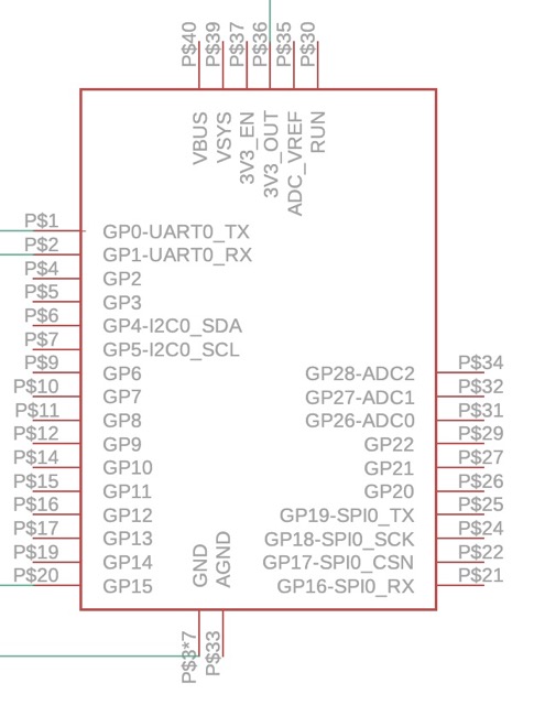
For this week's project, I chose to use the PICO W microcontroller by Raspberry Pi, thinking it would strike the right balance between great docs and resources online, native simplicity, wireless access, and enough pins for the sensors I want to use down the line. In Fusion, below is the
Schematic
> visual of the component:
This image is very sparse, and it's useful for diagrammatic organizing but I did find it difficult to learn from because it's so abstract. For example, it took me a while to understand that some of the pins on the left side are missing (it skips from pin 2 to pin 4 for example) because these are connected to ground, and therefore not available for connections in the schematic.
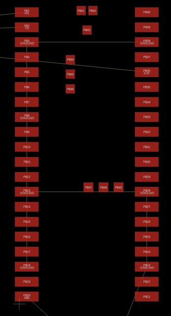
Meanwhile, in the
PCB
> representation above, the ground pins reappear. This visual is one step more physically realistic because it deals with the necessary factors for fabricating the PCB, including the footprints of the components and the tracking between them. Here, you can see the physical outline of the design even though most of the maneuvering of components needs to happen iteratively on the schematic side: that is, in order to change a connection between two components, they should be modified using the logic labels on the schematic first, so that their lines will reorganize automatically on the PCB interface.
Even though the PCB representation is slightly more literal relative to the fabrication of the board, it still doesn't show very clearly what the components look like. For this, it is necessary to also consider the
Pinout
of the microcontroller, published by its manufacturer.
The pinout shows all fo the labeled components of the board on a visual representation that looks just like the actual physical component, without abstracting away any connections. After some difficulty understanding the information represented by the design environments, it became clear that this ground truth is essential to effective PCB design; at least for myself, it is not possible to work from the abstractions alone.
Designing an Embedded Microcontroller System
Considering the aspirations of my Final Project to integrate depth and moisture sensors with location tracking, I wanted to design a PCB this week that could serve as a first draft for that more complex version later. Since the sensor components other than the GPS module may not be physically attached to the board, I focused on designing a GPS board first. The basic idea is to have a button that you can press to record a GPS location at the present position and time, and that a little LED will light up with successful measurements.
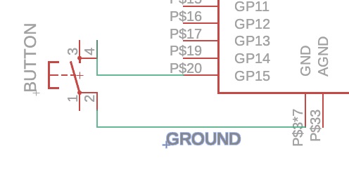
To create this, I first brought in the PICOW component from the fab tool library. As a first peripheral component, I added a button using the
SW_SWITCH-TACTILE_2PIN
component from the library, and I connected it to the PICOW by Pin 20 and Ground.
This would be the on-board button that could test the GPS. Next, I wanted to connect the GPS module. The module listed in the Full Class Inventory is this one. It connects to the board with 5 pins but is not ultimately an embedded PCB component, so I added a 5-pin pinhead to the board in order to support it.
The pin I did not connect directly to the PICO-W; instead I just labeled the different pins for TX (transmit), RX (receive), 3.3 Volt power, PPS (Pulse per Second, for timekeeping), and Ground. I labeled pins 1 and 2 on the PICO to be TX and RX, as it was indicated in their names on the board. For PPS, it can be connected to any GIPO pin but Google said that GPIO 4 would be typical, so I followed suit.
At first I wasn't sure on the schematic which pin was actually Pin 4, since the labels starting with "P" and those starting with "G" were different. However, on the PCB viewer the PPS pin was labeled, so I stuck with P$4. Anthony had pointed out that even when pins are interchangeable, one should never use a named pin when you only need a basic one-- I assume that the converse applies, that when the named pin is available one should use it.
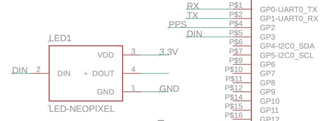
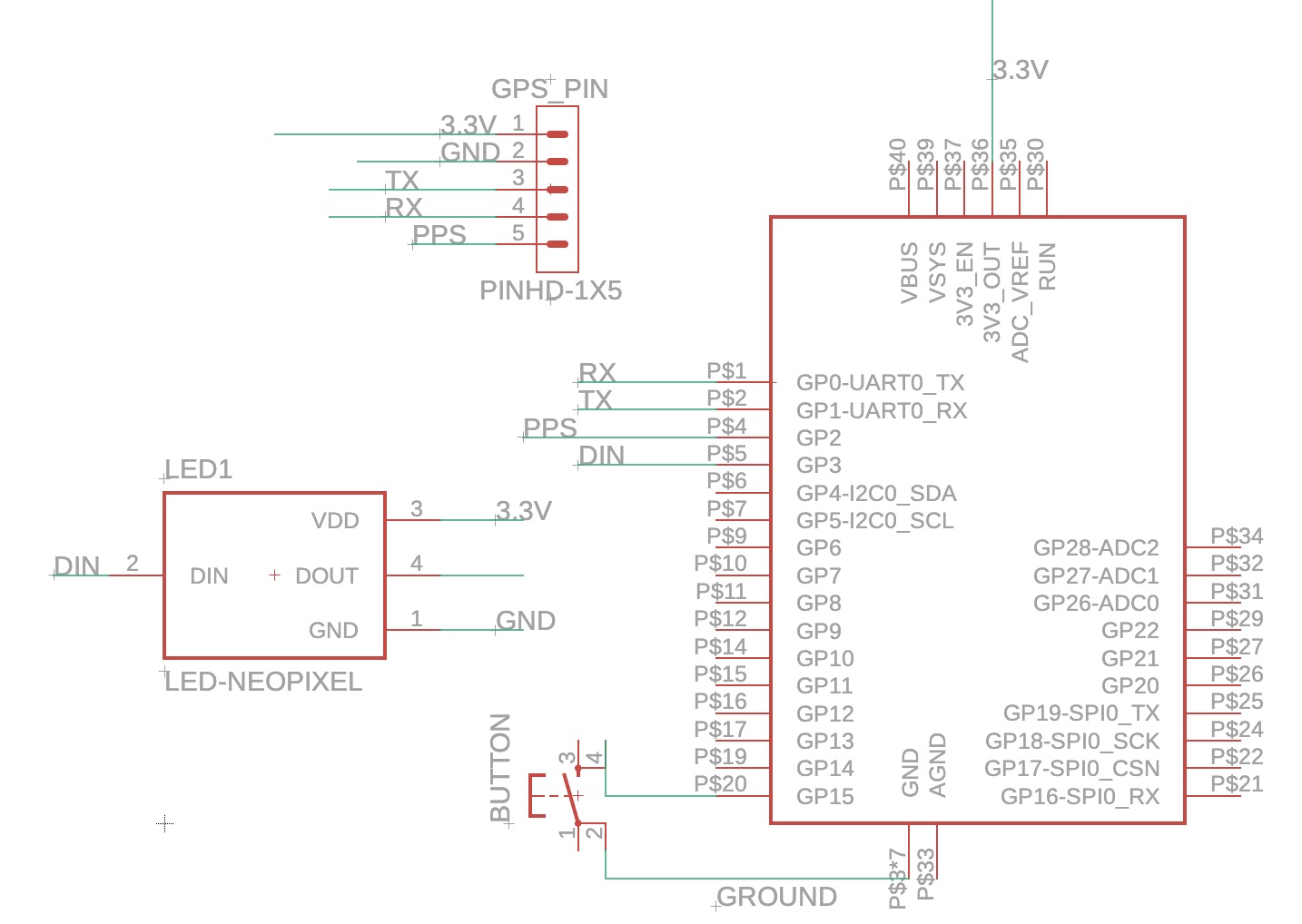
Next I connected an LED to the board, placing it next to the GPS pinhead. I also designated pin P$5 as the DIN for this element and connected it to power and ground.
With these components, the basic functionality of my board was in place, and in the schematic all the parts I needed for now seemed to be available:
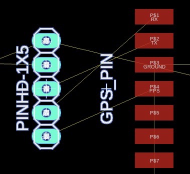
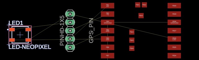
At this point, I moved to the PCB viewer in order to lay down the tracking. At first my LED and GPS pinhead were very tangled, with "air wires" overlapping in confusing ways:
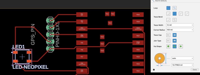
I rotated and moved the elements so that the wires would not be overlapping (this also required switching some of the pin names in the schematic so that they would reshuffle on the PCB, including the DIN on the microcontroller which I moved to pin P$9), and then I used the "route" function to put them in place, using 12 mil traces:
Design Rules for Fabrication
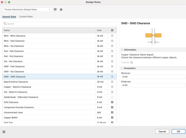
With the routes in place, I ran "DRC" in the command line to run a design rule check. When the menu came up I followed Anthony's directive to change the first six parameters (for wire clearance and via clearance) to 16 mil, and then ran the check.
I received 39 Copper Clearance errors which surprised me because they were for routes that Fusion did automatically! Running
ratsnest
to automatically clean things up did not fix them.
Since the issue was components being too close to one another, I moved some more pins around and re-routed everything together giving it much more space to breathe. I do note that the resulting organization seems far from optimal, but I couldn't figure out how to get the GPS pinhead and the LED to cooperate with the locations of the 3.3v and TX / RX pins without overlapping wires:
Simulating Operation
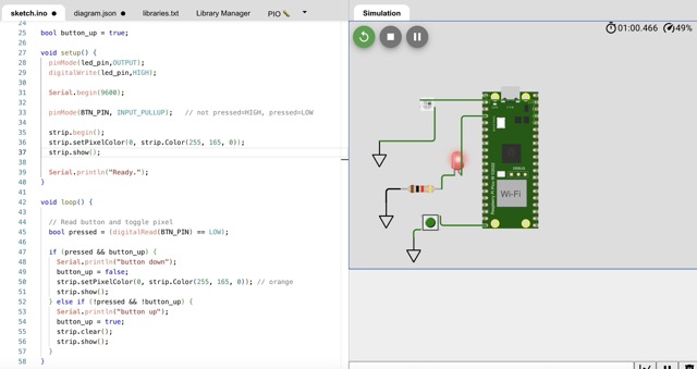
In the spirit of spiral development, I started simulation in Wokwi by implementing Neil's button test button LED demo, specifically the Arduino version (not micropython). This was a straightforward starting point (and demonstrated to me that the correct pin indexing is the GP numbers, not the straight numeric ones).
Since Wokwi does not have the GPS module, my board would do essentially the same thing as this example (bypassing the GPS reading so that the button just turns on the LED directly) except that it uses a neopixel LED. So I set about changing it so that the button would illuminate this different component.
While it would seem straightforward to simply exchange and rewire one component, this proved a major hitch because the neopixel requires different adafruit libraries, different wiring, and therefore new debugging. I encountered a situation of changing only a few things but between an unresponsive serial monitor, an unresponsive LED, and new code, being completely lost about how to debug the combined system...
Above is my new test, with a regular LED per Neil's example that I turn on in setup to ensure that the code is running even though my serial monitor is not. The Neopixel is also supposed to be turned on in setup, but I have never succeeded in getting it to respond, either to hard coded illumination or to manipulation by the button. As of class on October 8th I have not figured this out yet!
Testing Operation of a Microcontroller
The following is a link to our Group Assignment. Anthony and I had experimented with the multimeter on my project in Week 3, but this was a more in-depth review of assessment methods for determining the way a PCB works (or doesn't).
Trials and Tribulations
Following are some observations of the process this week, and some challenges or disappointments to record:
While I ultimately figured it out more or less, it took me a long time to understand what the PCB design interfaces show and what they don't. Without the intuition of electrical engineering in mind, I found it difficult to grasp what details they would be omitting.
I think my PCB is not very efficient-looking due to the trace that goes all the way around the board for the 3.3V connection of the GPS pinhead. This was necessary to avoid any overlap with the USB cable to the Pico or overlaps with other wires, and because I couldn't manage to get traces underneath the microcontroller while complying with the design rules.
I struggled mightily with the simulation this week, and part of my frustration with this was my uncertainty as to whether the problems I encountered in Wokwi were *real* problems (that would present the same way on a physical board implementation) or *fake* problems arising from misuse or limitations of the interface.
Learnings and Progress
Below is the delta between where I started on the skills for this week and where I arrived:
I had never designed a PCB before and learned a lot about the components that go on them, how they interact with one another, and the principles of electrical design in doing so. Cool!
Through the simulation I became more comfortable with Arduino code and debugging.
Resources and Acknowledgments
Thank you again to Anthony for going over the design with me individually, as I could not join the group office hour after recitation this week.
In debugging my simulation I did attempt to consult ChatGPT although no part of the linked conversation was actually helpful.
Design Files
My Fusion / Eagle files are in the course cloud folder online
And here are the sketch .ino and diagram .json that I was using in Wokwi.
 This image is very sparse, and it's useful for diagrammatic organizing but I did find it difficult to learn from because it's so abstract. For example, it took me a while to understand that some of the pins on the left side are missing (it skips from pin 2 to pin 4 for example) because these are connected to ground, and therefore not available for connections in the schematic.
 Meanwhile, in the
 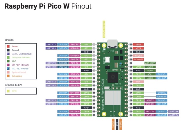 The pinout shows all fo the labeled components of the board on a visual representation that looks just like the actual physical component, without abstracting away any connections. After some difficulty understanding the information represented by the design environments, it became clear that this ground truth is essential to effective PCB design; at least for myself, it is not possible to work from the abstractions alone.
 This would be the on-board button that could test the GPS. Next, I wanted to connect the GPS module. The module listed in the Full Class Inventory is this one. It connects to the board with 5 pins but is not ultimately an embedded PCB component, so I added a 5-pin pinhead to the board in order to support it.
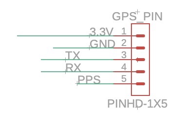 The pin I did not connect directly to the PICO-W; instead I just labeled the different pins for TX (transmit), RX (receive), 3.3 Volt power, PPS (Pulse per Second, for timekeeping), and Ground. I labeled pins 1 and 2 on the PICO to be TX and RX, as it was indicated in their names on the board. For PPS, it can be connected to any GIPO pin but Google said that GPIO 4 would be typical, so I followed suit.
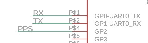 At first I wasn't sure on the schematic which pin was actually Pin 4, since the labels starting with "P" and those starting with "G" were different. However, on the PCB viewer the PPS pin was labeled, so I stuck with P$4. Anthony had pointed out that even when pins are interchangeable, one should never use a named pin when you only need a basic one-- I assume that the converse applies, that when the named pin is available one should use it.
 Next I connected an LED to the board, placing it next to the GPS pinhead. I also designated pin P$5 as the DIN for this element and connected it to power and ground.
 With these components, the basic functionality of my board was in place, and in the schematic all the parts I needed for now seemed to be available:
 At this point, I moved to the PCB viewer in order to lay down the tracking. At first my LED and GPS pinhead were very tangled, with "air wires" overlapping in confusing ways:
 I rotated and moved the elements so that the wires would not be overlapping (this also required switching some of the pin names in the schematic so that they would reshuffle on the PCB, including the DIN on the microcontroller which I moved to pin P$9), and then I used the "route" function to put them in place, using 12 mil traces:
 I received 39 Copper Clearance errors which surprised me because they were for routes that Fusion did automatically! Running
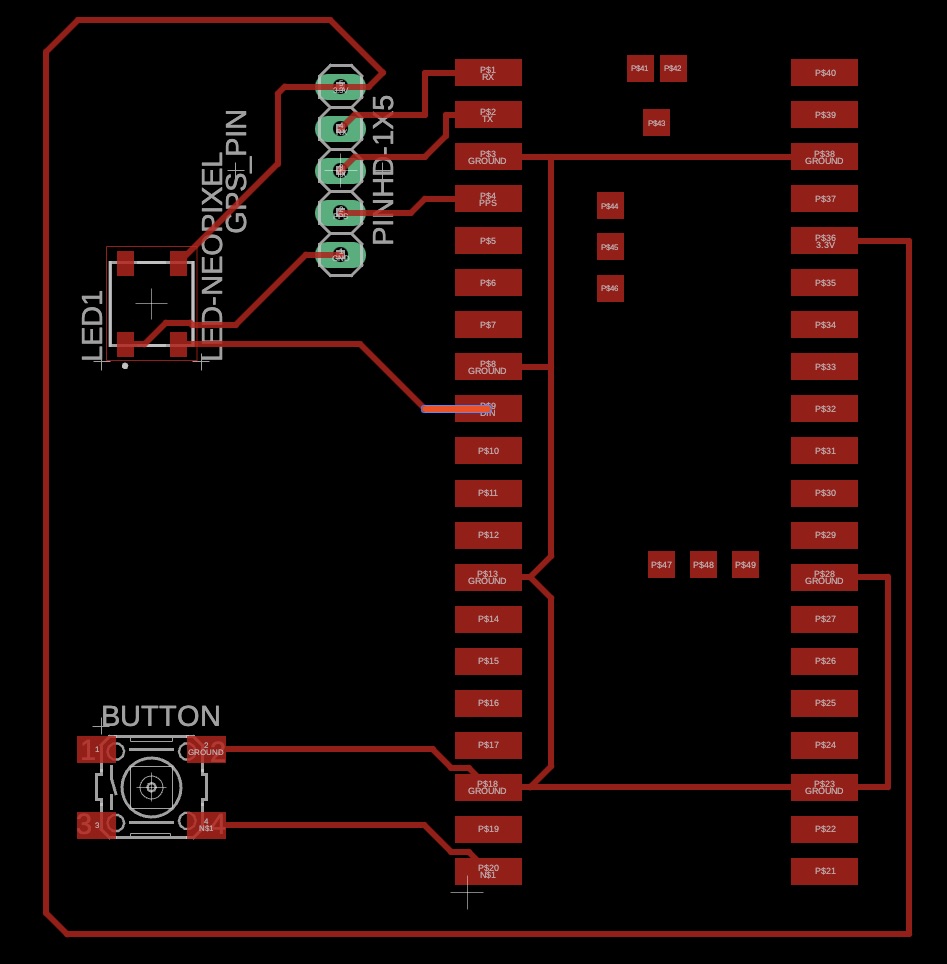
 Above is my new test, with a regular LED per Neil's example that I turn on in setup to ensure that the code is running even though my serial monitor is not. The Neopixel is also supposed to be turned on in setup, but I have never succeeded in getting it to respond, either to hard coded illumination or to manipulation by the button. As of class on October 8th I have not figured this out yet!