Week 5
AVR DU
I chose to focus on the AVR DU family of microcontrollers. These microcontrollers are based on the 8-bit AVR CPU and can run at up to 24MHz. Notably, they also include USB 2.0 support. Although they are not currently part of the inventory, I believe these microcontrollers will be a good addition in the future.
I initially focused on CPN AVR32DU28T-I/SS.
The 32 indicates 32KiB of Flash, 4KiB of SRAM and 256B of EEPROM
(there are also 16 variants, with half the Flash and SRAM,
and 64 variants, with double the Flash and SRAM).
The 28 indicates 28 pins, including 21 GPIOs.
The larger 32-pin variants add 4 more GPIOs (and ADC channels);
there are also 14- and 20-pin variants.
The SS indicates that this is the SSOP package.
This same chip is available in VQFN and SPDIP packages as well.
Other variants are also available in SOIC and TQFP packages.
KiCad Library
The first step was adding this chip to the fab KiCad library.
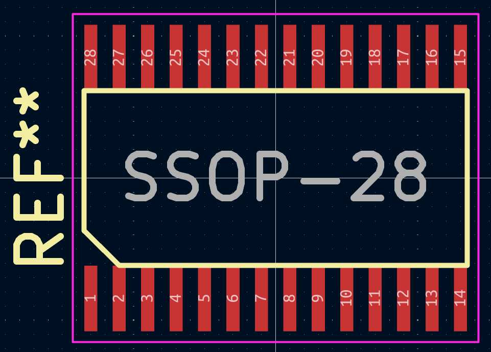
I created a SSOP-28_3.9x8.8_P0.65mm footprint,
which I based on the existing SSOP-16_3.9x4.9_P0.65mm footprint.
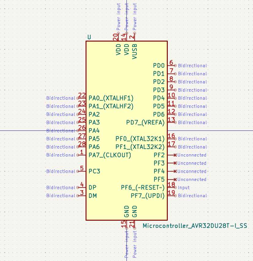
I created a Microcontroller_AVR32DU28T-I_SS symbol from scratch.
I included the 4 pins that exist on the 32-pin variants as NC. This way, if we decide to upgrade to one of those variants, or add one of those variants to the inventory, existing schematics can be updated with a drop-in replacement symbol.
Schematic
Basics
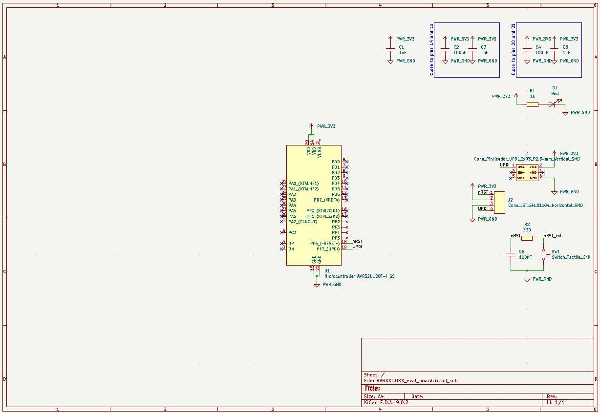
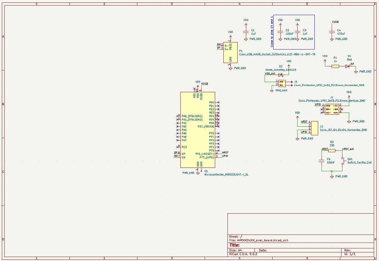
The second step was creating a schematic. I started with Chapter 4 of the datasheet to get decoupling, reset and programming down:
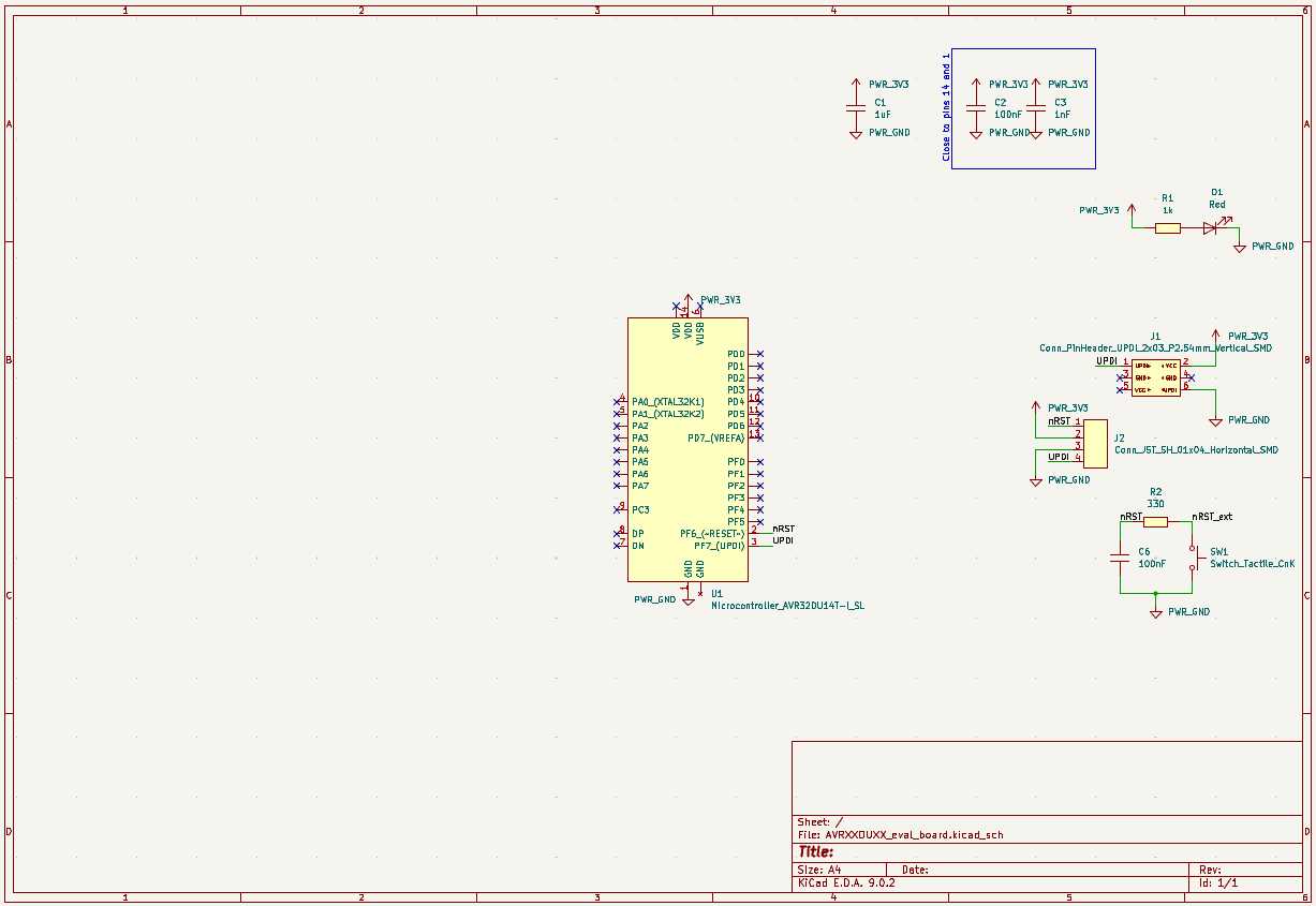
Then I realized that the package we had in hand was the 14-pin SOIC
(AVR32DU14T-I/SL).
So, I made a new Microcontroller_AVR32DU14T-I_SL symbol,
and linked it to the existing SOIC-14_3.9x8.7mm_P1.27mm footprint.
I updated the schematic and removed one set of decoupling caps:
Power
Then I had to figure out a power supply scheme.
The chip has two power domains available externally - VDD and VUSB,
on pins of the same names.
VDD supplies the I/O structures, the internal oscillator, and the regulator driving the core
(the two pins on the larger variants are shorted internally, as are the GND pins).
VUSB seems to only power the USB transceiver.
It has to be 3.3V (not 5V).
There is a regulator on chip that can generate it,
as long as VDD is at least 4.5V.
The datasheet doesn’t spec the regulator, so I can’t rely on it as an output pin for peripherals.
Furthermore, the transceiver is only in use when the device is connected over USB,
and there is always 5V available when the device is connected over USB.
So, it seems to me that the VUSB pin is only useful in two scenarios:
- I want
VDDto be less than 4.5V even when 5V from the USB connector is available. In this case, I would need off-chip 3v3 regulation (for which the USB’s 5V is available if needed) - I care about efficiency and want to generate 3v3 in a more efficient manner than it would be from the (presumably) linear on-chip regulator
I want the board to be able to run off of USB alone, and there is no reason for now not to have VDD at 5V in that case, since energy efficiency is not a concern and I have not added any 3v3 peripherals. So, I simply connect a 470nF cap to the pin, as recommended in Table 36-2 in the datasheet.
I want the board to be able to run off of an external supply as well,
so I added a header for that.
To prevent reverse current in the scenario where both supplies are connected,
I added a Schottky diode to the external supply
(the voltage drop is okay in this scenario, so a fancier scheme is not necessary).
Of the three devices in the inventory, I chose BAT46ZFILM
because it was the only one for which I could find a SPICE model
(see Simulation section below).
I changed out the fab:PWR_3V3 symbol for the generic power:VDD symbol throughout
to communicate to the reader that the voltage is not set.
Finally, I added a USB port.
I used the mini port because I find it a little easier to solder on.
Peripherals
With everything needed to run the chip, it was time to add some peripherals.
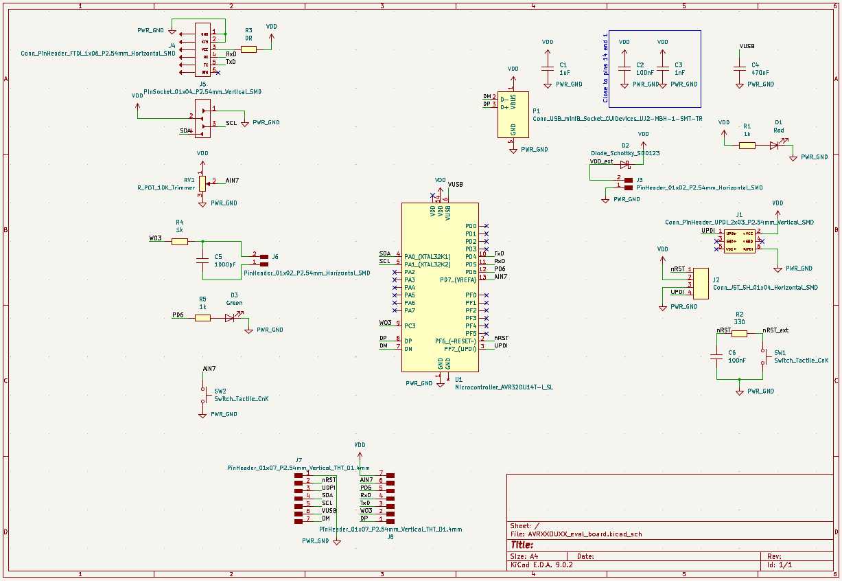
The first was UART. Serial communication should be possible over USB,
but I don’t want to have to bring up USB to be able to do serial debug.
Referring to the table in 3.1 of the datasheet,
the default pins for USART0 are 4 and 5,
but those are the only pins available for TWI on the 14-pin variant.
I picked 10 and 11 instead, which are firmware-selectable alternatives.
I decided to forego the sync pin (XCK0) and flow control pin (XDIR0).
I placed the UART pins onto the middle 4 pins of a 6-pin connector with what I think is
pretty standard ordering.
I added a removable 0R in line with the power in case we want to disconnect that.
Next, I hooked up a header for TWI (to test I2C). I used the OLED pinout from the inventory so that one of those screens can be plugged in easily.
Next, I wanted to have a way to test the ADCs.
I picked pin 13 for the ADC test, because that’s also the VREFA pin.
I added a trim pot to that pin.
Next, I wanted to test the Timer Counters.
The only pins left were 9 and 12, but only 9 had a TC output, so I picked that.
I added a simple LPF to smooth out the PWM output and create an analog value, kind of.
I picked a cutoff frequency of 159kHz.
This is above 20kHz to allow for audio, but relatively low to minimize ripple.
I picked R=1k so that it doesn’t compete with any parasitic resistance (which would lower the cutoff),
so C=1000pF.
I added a connector to the output.
The eval board was still missing the two most basic peripherals: a button and an LED. I didn’t want to use the UDPI and Reset pins, to keep things simple. So, I added the LED to the last free GPIO (pin 12), and I put the button on the same pin as the trim pot (which can be set to double as a pull-up).
There are of course other things to evaluate. Notably: comparators, SPI, the event system and the configurable custom logic. The listed on-board hardware provides functionality for most basic evaluation, however.
Direct pin access
Finally, I wanted to provide easy access to the pins directly. This can be used to read out voltages on a logic analyzer or oscilloscope, drive voltages directly from a power supply or function generator, or attach additional peripherals. I spaced the headers in a multiple of 100 mils to allow for easy compatibility with obsolete technology.
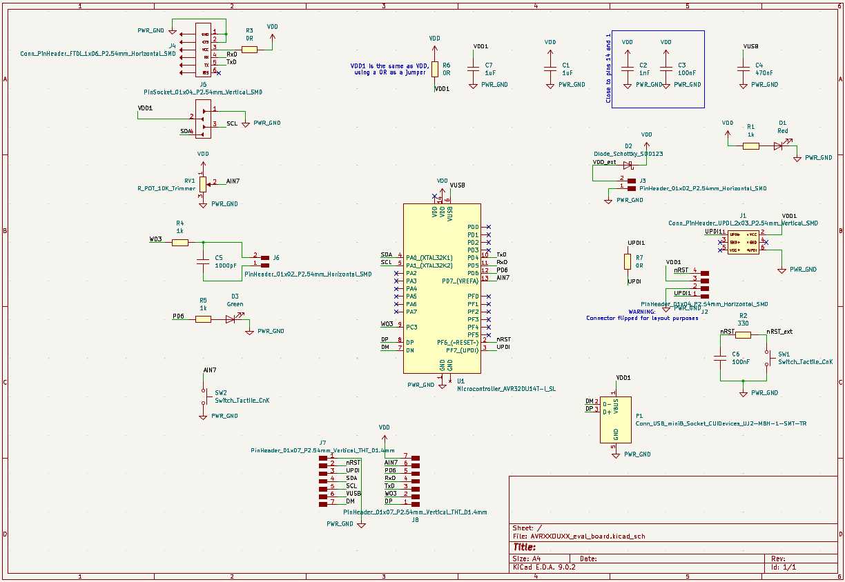
The updated schematic is shown below:
Simulation
Instead of simulating the entire circuit, I simulated functional blocks.
I had never used ngspice before, so I took this opportunity to learn a new tool.
I am documenting what I learned here.
I installed ngspice directly from the Debian Trixie package repos.
I got a downstream of version 44.2 which is only one major version behind upstream,
and was released in January of this year - impressive turnaround for Debian stable!
$ ngspice -v
******
** ngspice-44.2 : Circuit level simulation program
** Compiled with KLU Direct Linear Solver
** The U. C. Berkeley CAD Group
** Copyright 1985-1994, Regents of the University of California.
** Copyright 2001-2024, The ngspice team.
** Please get your ngspice manual from https://ngspice.sourceforge.io/docs.html
** Please file your bug-reports at http://ngspice.sourceforge.net/bugrep.html
** Creation Date: Sun Jan 12 08:19:15 UTC 2025
******
I tried using ChatGPT to learn how to use the tool, but I was not able to get much useful information from it. (At the end of our conversation, the chatbot gave me a nice wish: “All the best with your work in MAS.863 — sounds like a fun course!”. MAS.863 is definitely a fun course, but I don’t remember mentioning it. Maybe I did in my ChatGPT attempt last week. Does it refer to prompts from previous threads? This gives me a very uneasy feeling.) I will keep practicing good prompt engineering, but for now I turned to the official documentation, which was clear and succinct. I also found the tutorials on the official website to be pretty good.
Schottky
Having figured out ngspice, I started simulating functional blocks.
The first block I looked into was the dual power supply.
Specifically, I wanted to use SPICE to pick one of the three available Schottky diodes.
Unfortunately, I only found
a model
for BAT46ZFILM.
It is technically for BAT46W, but based on the
datasheet,
it seems to be the same diode in a different package.
I ran the simulation for 6 different loads. I used section 10 of this tutorial to figure out how to iterate over different loads. The script I came up with is given below:
Test of available RBC devices

.model DI_BAT46W D(IS=603n RS=0.280 BV=100 IBV=5.00u CJO=7.96p M=0.333 N=1.70 TT=7.20n)

VDD vdd 0 DC 5

VDDEXT vddext 0 DC 5

D1 vddext vdd DI_BAT46W

R1 vdd gnd_r1 1k
VR1 gnd_r1 0 0

.dc VDDEXT 0 10 0.01

.control
let plotstr_vddext = ' '
let plotstr_vdd = ' '
let plotstr_vr1 = ' '
foreach load 1 10 100 1k 10 100k
    alter R1 $load
    run
    set plotstr_vddext = ( $plotstr_vddext {$curplot}.i(VDDEXT) )
    set plotstr_vdd = ( $plotstr_vdd {$curplot}.i(VDD) )
    set plotstr_vr1 = ( $plotstr_vr1 {$curplot}.i(VR1) )
end
plot $plotstr_vddext
wrdata output_vddext.csv $plotstr_vddext
plot $plotstr_vdd
wrdata output_vdd.csv $plotstr_vdd
plot $plotstr_vr1
wrdata output_vr1.csv $plotstr_vr1
.endc

.end
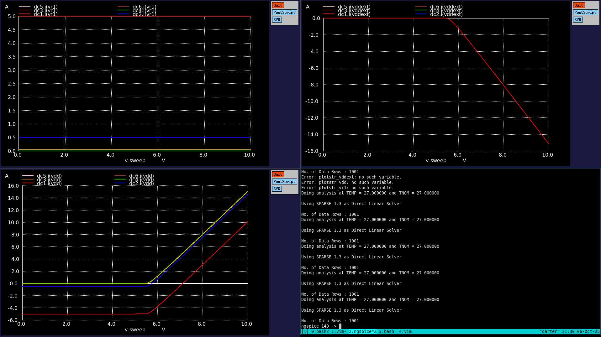
The output of the script is shown below:
Top-left shows the current through the load. Bottom-left shows the current through the USB port. Top-right shows the current through the external supply port. (Note that the latter two are negative; I couldn’t figure out how to flip them with this loop setup.) There are ways to make the plots prettier, but this validates the circuit for now: up until past 5V, this Schottky diode prevents reverse current.
I tried plotting these on a semilog plot,
but ngspice rightfully refused because of the existence of negative values.
So, I exported the data and
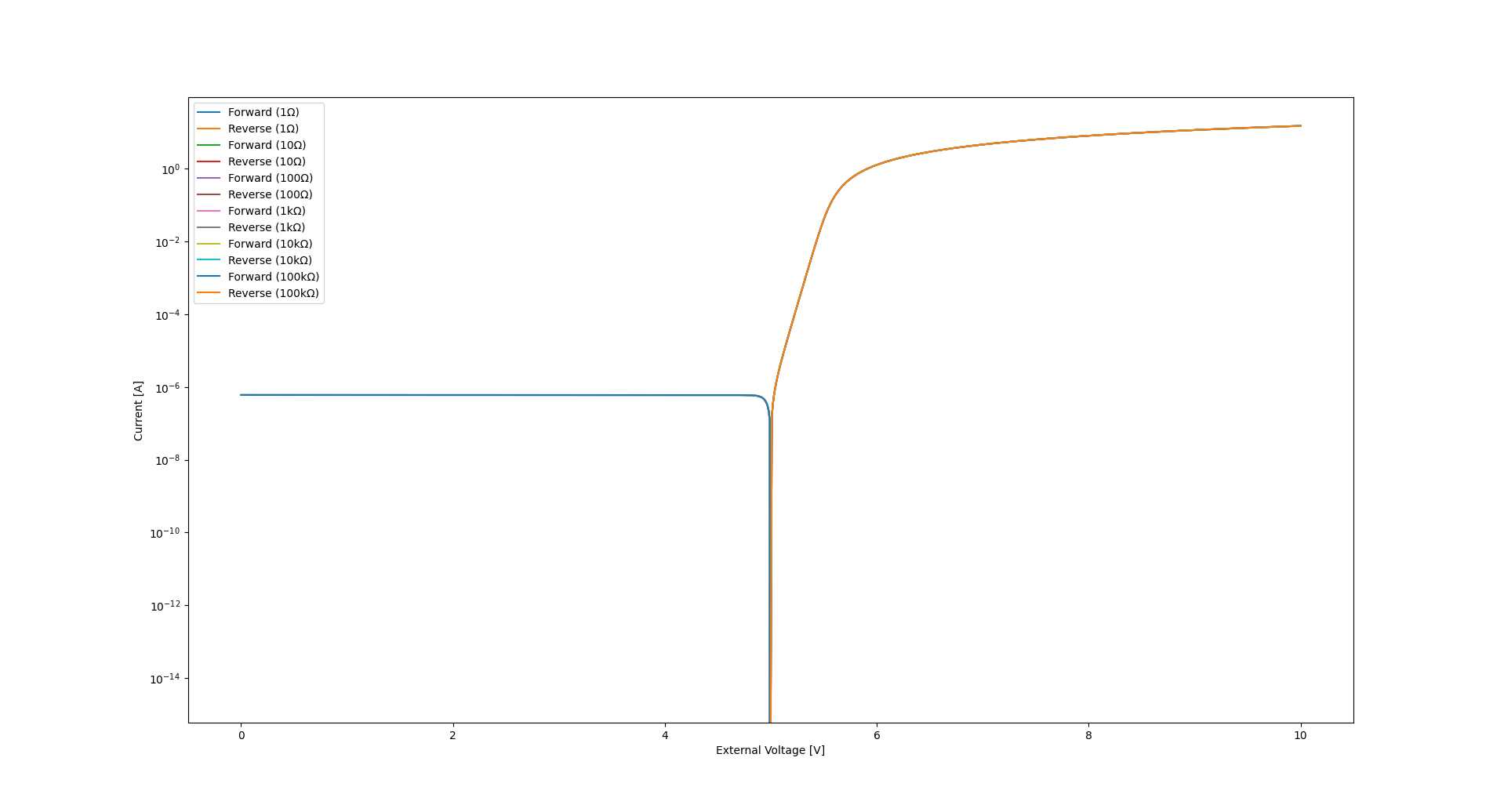
plotted the current through the external supply port using matplotlib,
which I’m more comfortable with:
This shows that for external voltages below 5V, the reverse current is only 1μA. It also shows that the behavior is not dependent on load.
Layout
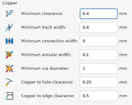
With the schematic done and simulated, I bagan layout. I used the design rules from recitation to start:
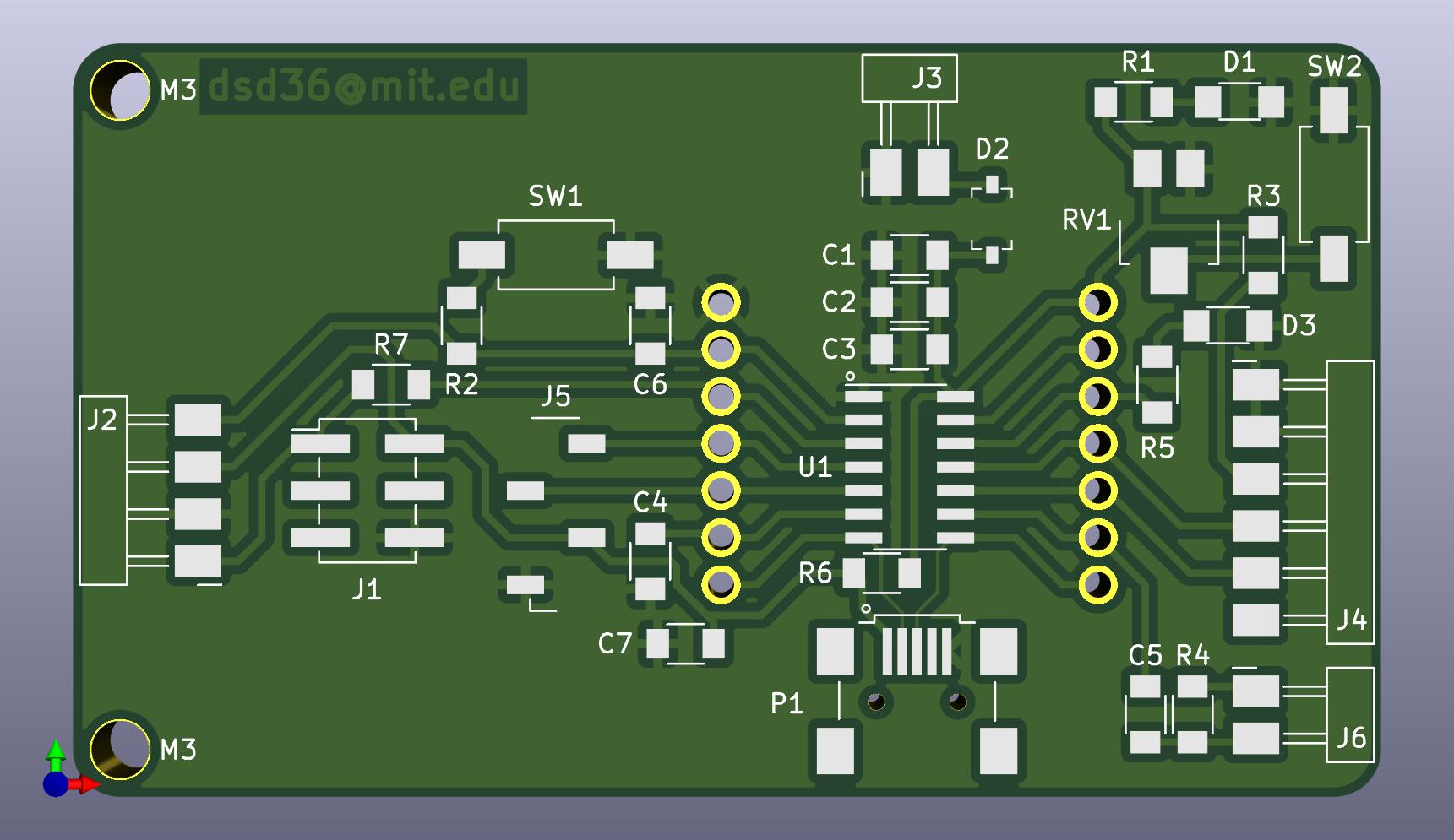
I placed the chip in the middle and the decoupling capacitors close to its power pins. I placed the USB mini connector on the other side, close to the USB data pins. I placed the pin headers alongside it, spaced 800 thau apart. Then, I placed all the components near the pins they connect to and routed them.
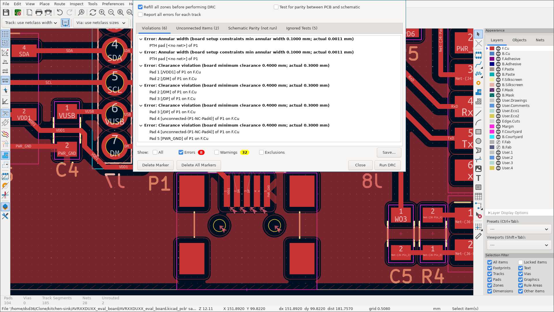
The only issue was the USB mini connector, which fails DRC out of the box:
I also had to add a few 0R jumpers. The final schematic is shown below:
The final layout is shown below:
