Turning digital schematics into physical reality
Serves: One ambitious electronics chef
Total Time: Several hours of exporting, milling, soldering, and fixing mistakes
This week I took the PCB I designed in Week 4 and moved it from the digital realm into the physical world. The first step was exporting the fabrication files from KiCad. From the schematic and PCB layout, I navigated to:
File → Fabrication Outputs → Gerbers
For desktop PCB milling, we only care about a small subset of these files:
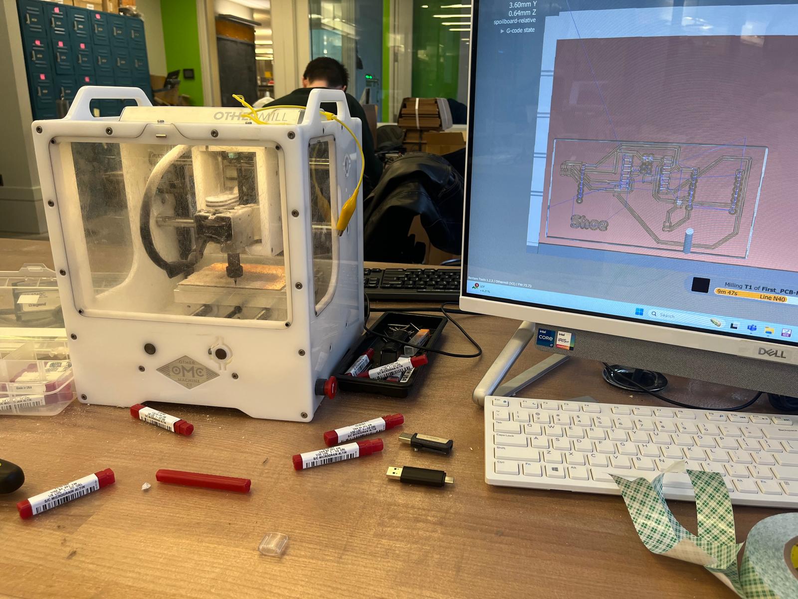
Once these files were generated, I transferred them to the lab computer connected to the PCB milling machine. At this point, the design was no longer abstract — any mistakes I had made in Week 4 would now become very real.
Before milling could begin, the machine itself had to be carefully prepared. I mounted a fresh copper-clad board to the mill bed using four strips of double-sided tape on the back. This step is deceptively important: uneven tape or poor adhesion can cause the board to lift mid-cut, instantly ruining the traces.
I aligned the copper board to the bottom-left corner of the sacrificial bed, making sure the edges were square. This alignment ensured that the origin in software matched the physical board location.
To set the machine’s origin and Z-height, I used the familiar yellow calibration tools. These were used to carefully find the corner of the board and establish an accurate Z-zero so that the end mill would remove just enough copper without cutting too deeply into the substrate.
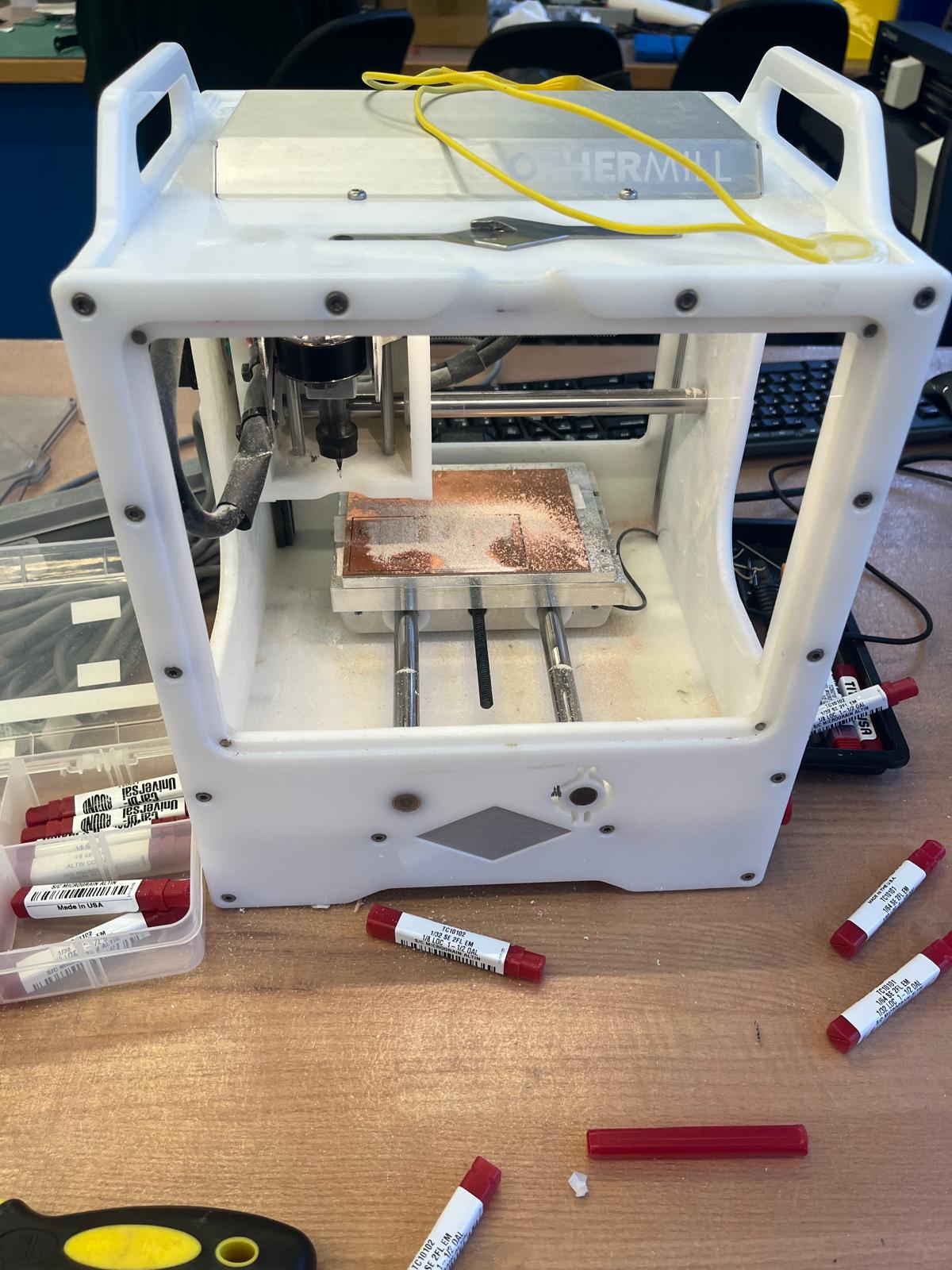
Milling a PCB is a multi-step process that requires different tools for different jobs. I began with a 1/64” flat end mill, which is used to mill the fine copper traces. This bit is extremely fragile, but it allows for clean isolation between closely spaced traces.
Once the traces were completed, I switched to a 1/32” PCB conservative end mill. This larger bit was used to cut out the board outline defined by the Edge.Cuts layer. Using a conservative toolpath reduces stress on the bit and minimizes the risk of snapping it during deeper cuts.
Each tool change required resetting the Z-height, and any mistake at this stage could destroy the entire board. This week taught me that patience and careful setup are far more important than speed.
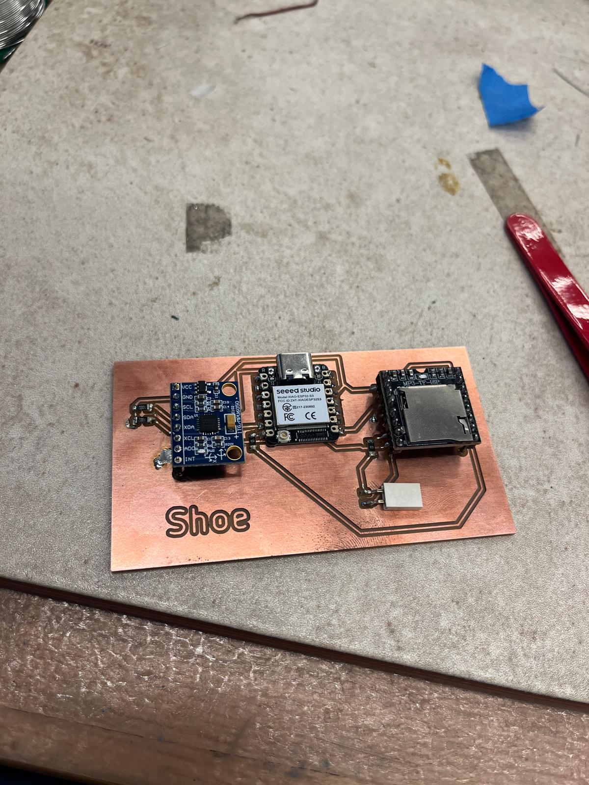
After milling, I carefully removed the board from the bed and inspected all traces under a microscope. Once I was confident that everything looked correct, I began soldering components onto the board.
I started with the smallest components first — resistors and capacitors — before moving on to larger modules like the ESP32-S3, MPU6050, and DFPlayer Mini. This ordering made it easier to access pads and reduced the risk of accidentally bumping already-soldered components.
During initial testing, I discovered a very small break in one of the copper traces. This tiny defect caused inconsistent behavior and took some time to diagnose. Once found, I was able to manually bridge the connection and restore continuity.

This week was a powerful lesson in how theoretical design decisions become physical realities. A trace that looks perfect on a screen can fail due to milling tolerances, tape placement, or tool wear. Electronics production is equal parts precision, patience, and problem-solving.
Successfully holding a working PCB in my hands for the first time was incredibly satisfying — and it laid the foundation for every input, output, and system integration project that followed.
For more details on how this board was used in later weeks, see Week 7 (Inputs) and Week 8 (Outputs).