Basic of Input Device
Group Assignment
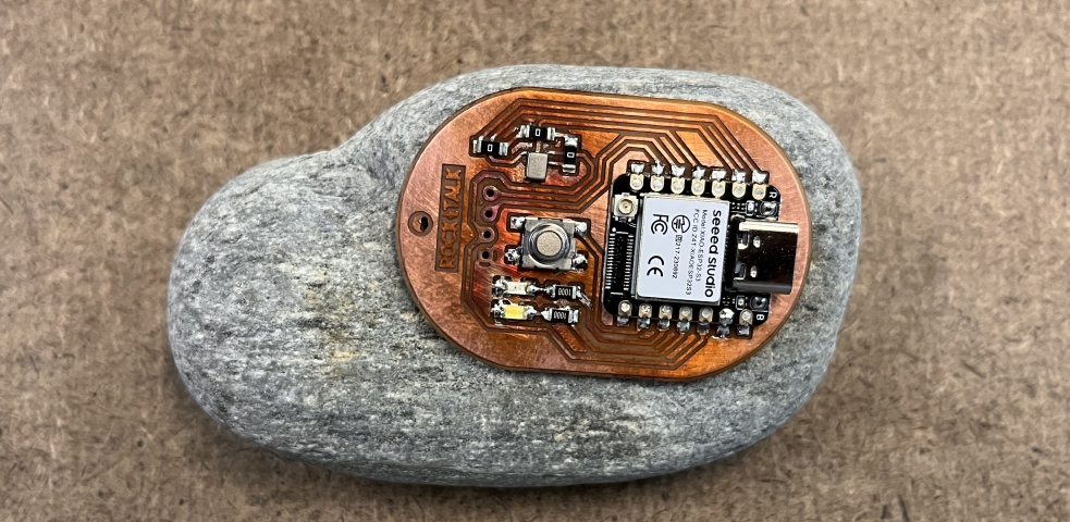
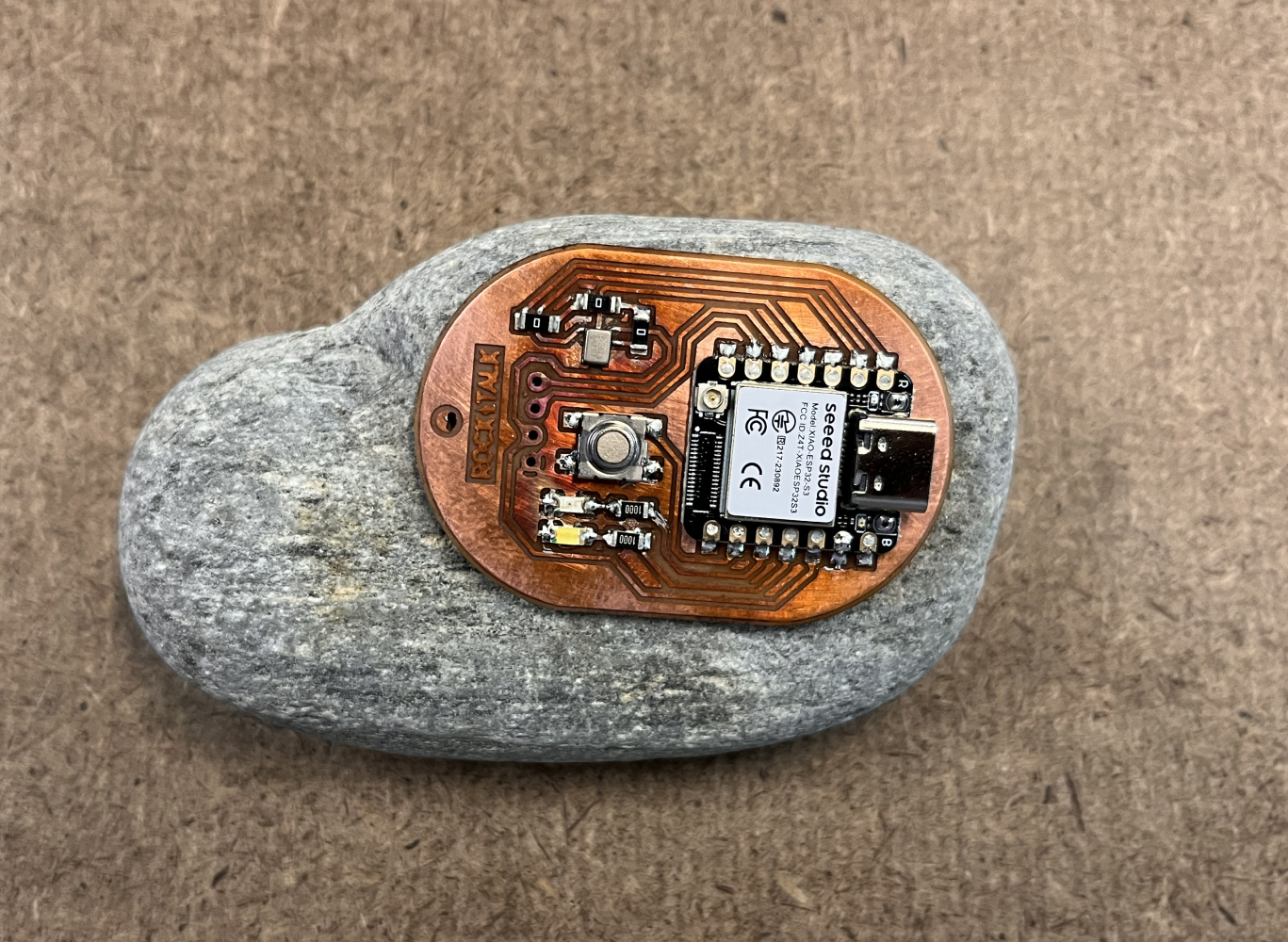
PCB Design
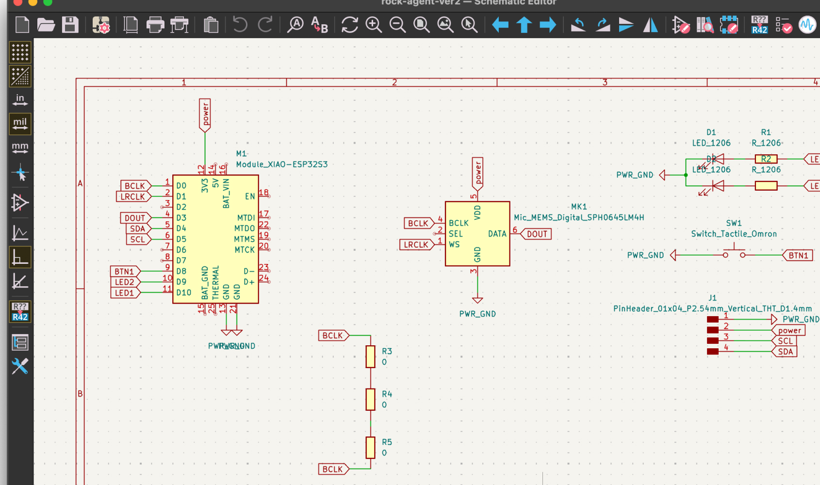
For PCB design, it was similar to previous week6 PCB Production week. To make the final PCB board for the rock device, I finalized the flow and the components.
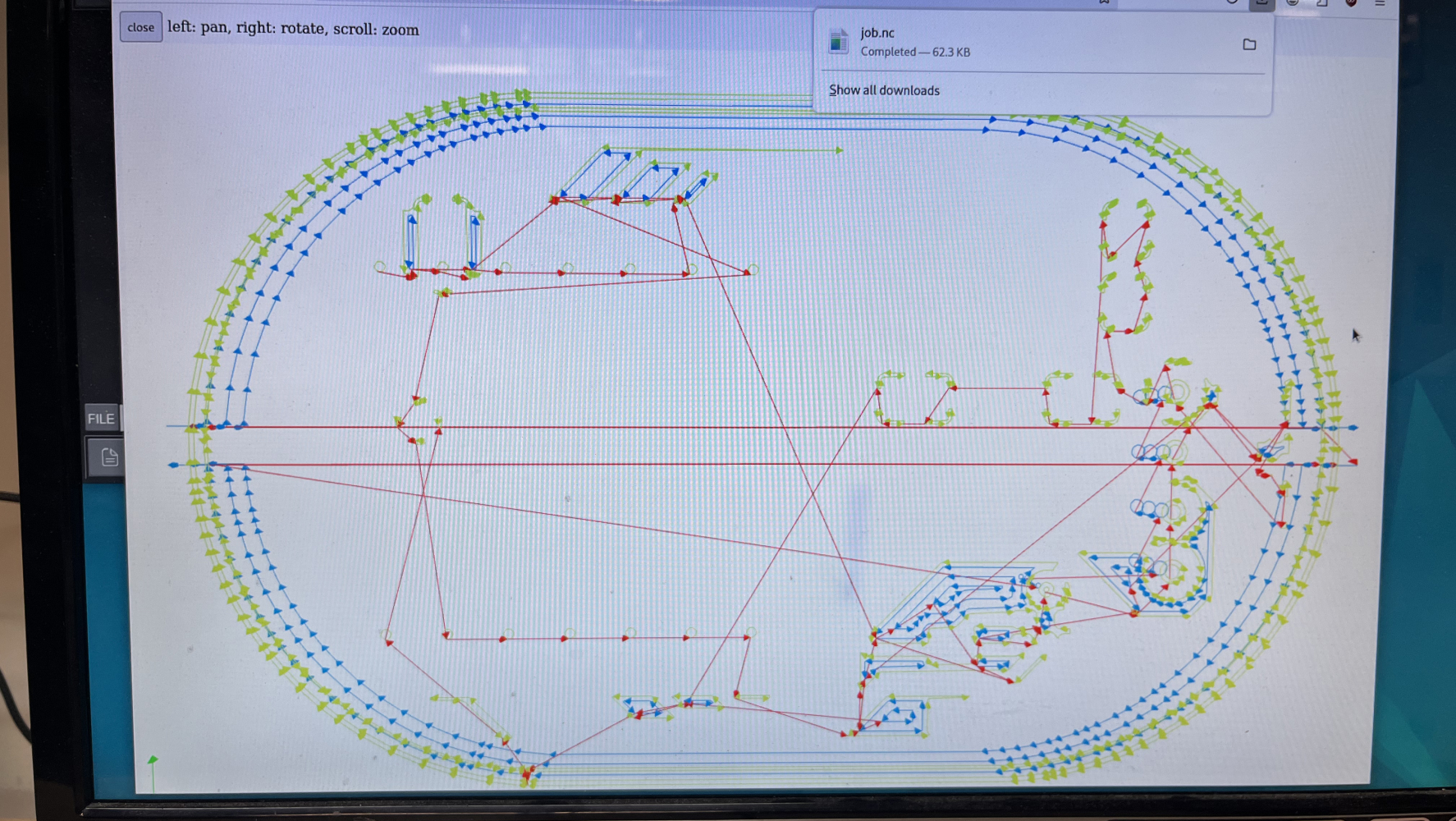
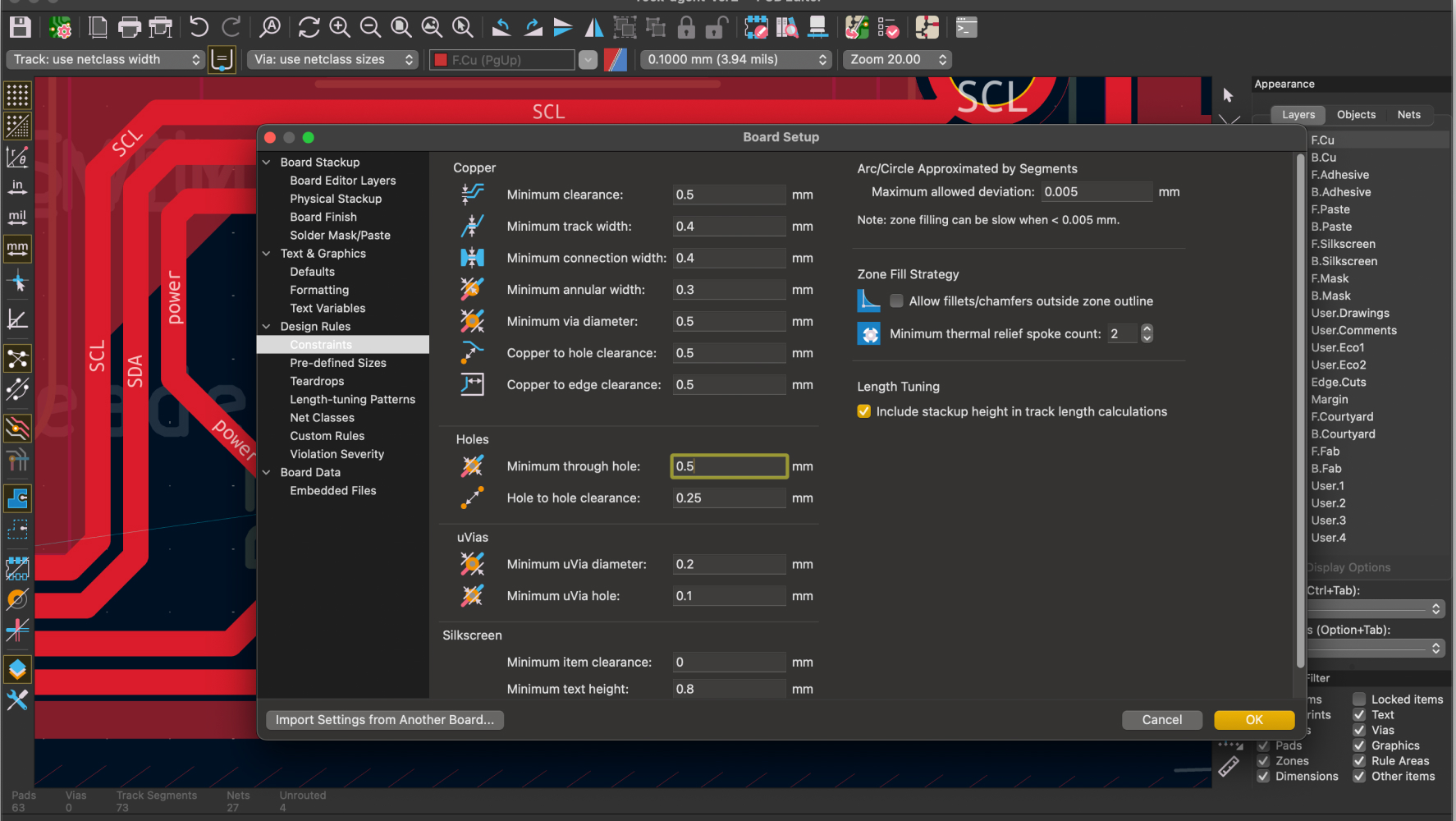
After implementing the design to cavera, I realized that I didn't initialized the design rules in the KiCad.... REMEMBER every time you open the new kicad file, you need to re-change the design rules that fit to your cavera machine, or you should import the design rules from your previous file as a template.
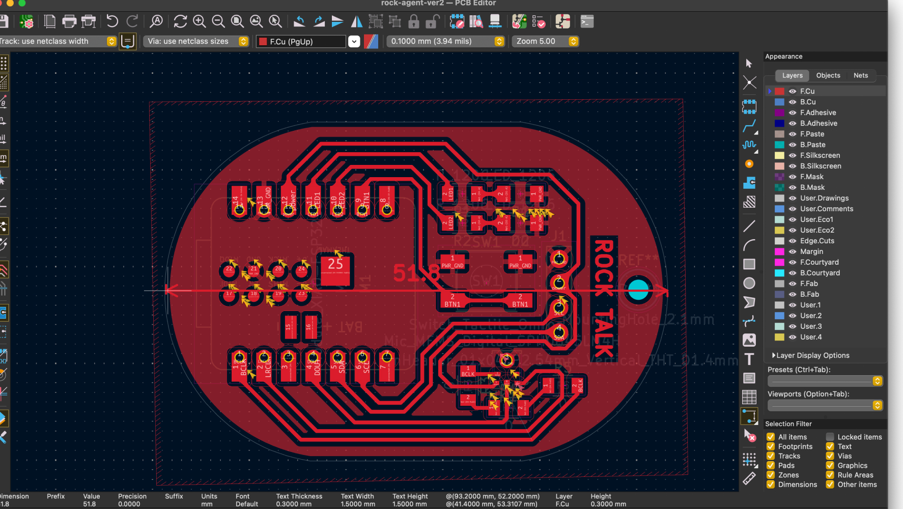
I checked the size of PCB to make sure it can be implemented inside the rock.
Soldering
Soldering Paste
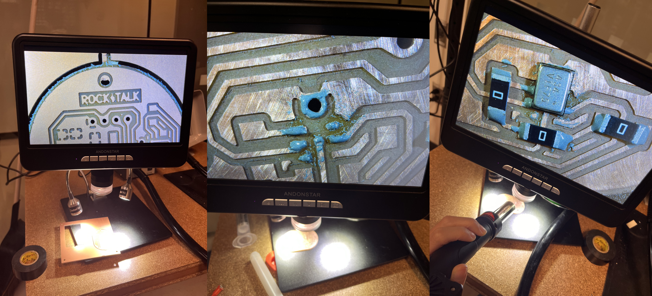
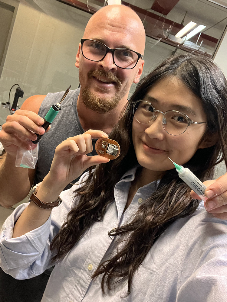
Thanks for Kristof for training the PCB design and soldering!
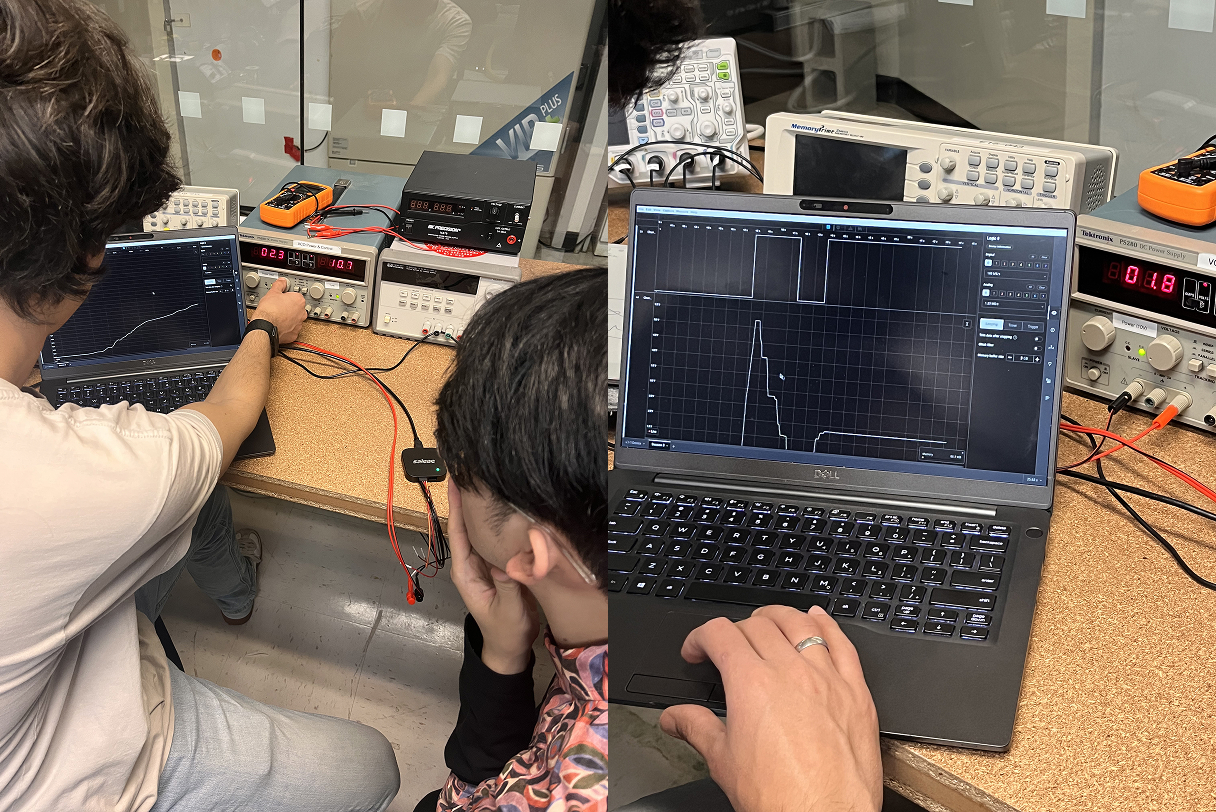
Test
After soldering all components, I tested the microphone input with the ESP32-S3. The LED responds to sound levels, confirming proper microphone functionality.
Appendix
Learning from Failures
- Always set Design Rules FIRST: Before starting any PCB layout in KiCad, immediately configure the design rules to match your milling machine capabilities (trace width, clearance, via sizes). Don't wait until after routing!
- Import design rule templates: Save time by importing design rules from previous successful projects rather than reconfiguring from scratch each time.
- Size verification is crucial: Check physical dimensions against your enclosure early in the design process, not after milling.
- Component orientation matters: Double-check microphone placement and orientation - the acoustic port must be accessible and properly positioned.
- Test points save time: Add test points for power rails and critical signals to simplify debugging with a multimeter.
- Breakout flexibility: Consider designing components on breakout boards for easier testing and replacement if needed.