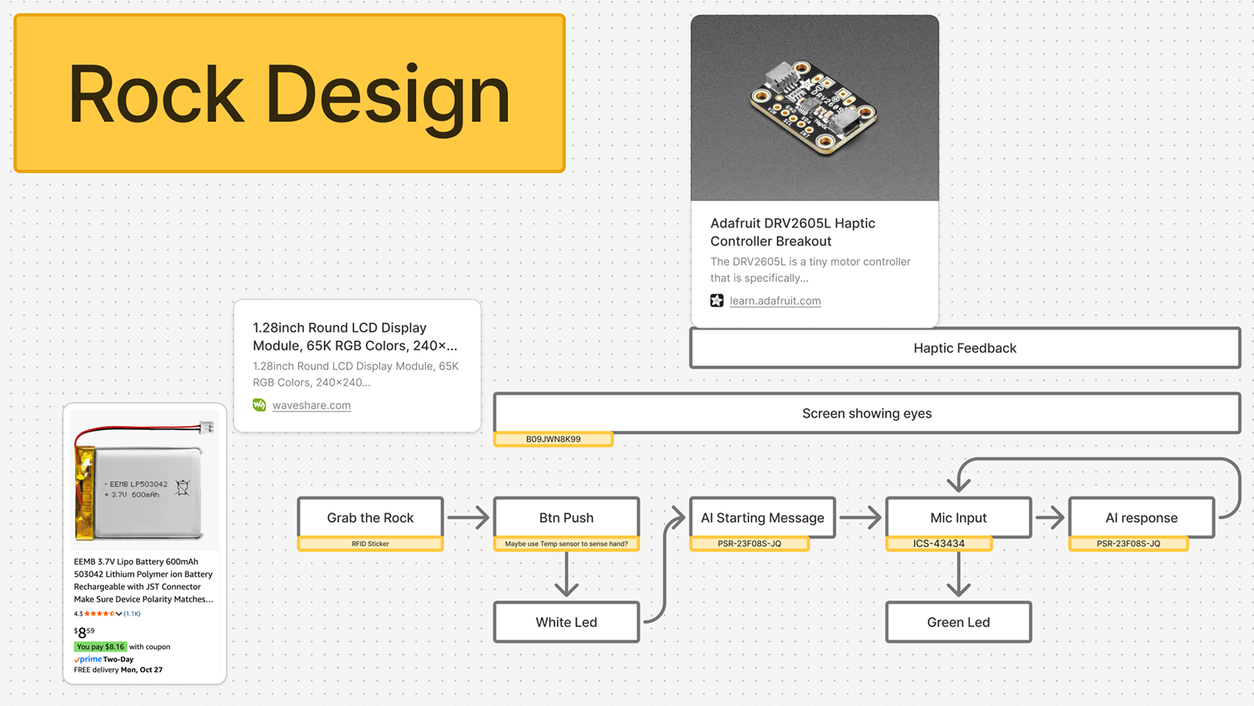
Project Overview
This week I developed the output systems for the Rock Talk device: an AI-responsive PCB that facilitates journal recording and provides multi-modal feedback through haptic vibration, audio output, and visual display.
Output Devices Integrated
- Haptic Motor: Tactile feedback for user interaction confirmation
- Speaker (MAX98357A): I2S audio output for AI voice responses
- Screen: Visual feedback and status information
Input Devices (from Week 8)
- Accelerometer: Motion detection for rock pickup
- Microphone: Voice input for conversation (see Week 8)
Group Assignment
CBA Shop Group Assignment
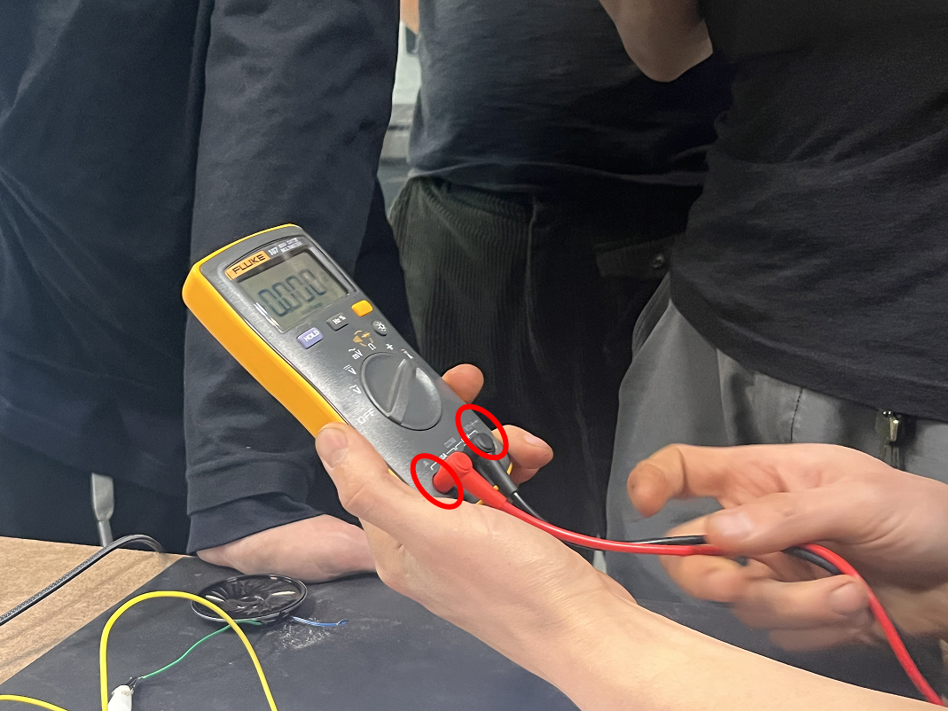
Our group tested various output devices including speakers, motors, and displays. We compared power consumption, response times, and output quality across different component types.
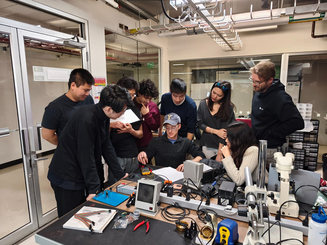
Testing audio output with oscilloscope to measure signal quality and frequency response.
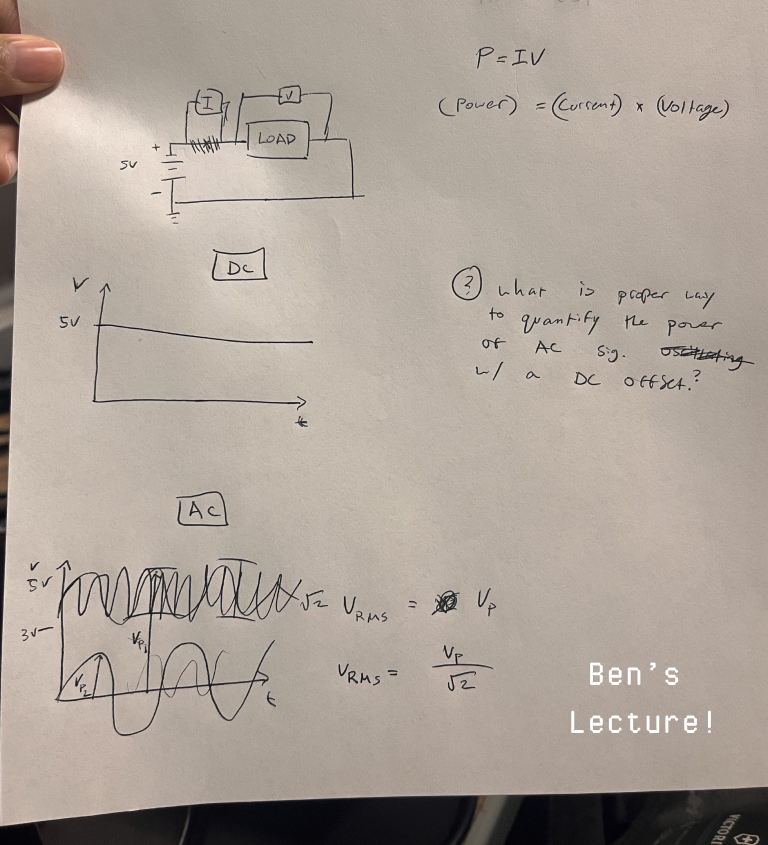
Comparing different speaker amplifier circuits and measuring THD (Total Harmonic Distortion).
Successfully tested speaker output with various audio signals. Confirmed proper I2S communication and audio quality.
Key Findings
- I2S audio: Superior quality compared to PWM-based audio output
- Class D amplifiers: More efficient than linear amplifiers (90% vs 60% efficiency)
- Haptic motors: Require proper current limiting to prevent damage
- Power considerations: Multiple output devices need careful power budget planning
Design & Milling
Design Philosophy: Modular Breakout Boards
After experiencing multiple failures with integrated PCB designs in previous weeks (see Week 3 and Week 8), I adopted a modular breakout board strategy for this week's output devices.
Why Breakout Boards?
- Testing flexibility: Each component can be verified independently
- Easy replacement: If a component fails, only that module needs replacement
- Iterative development: Allows testing different components without redesigning entire board
- Debugging simplification: Isolates problems to specific subsystems
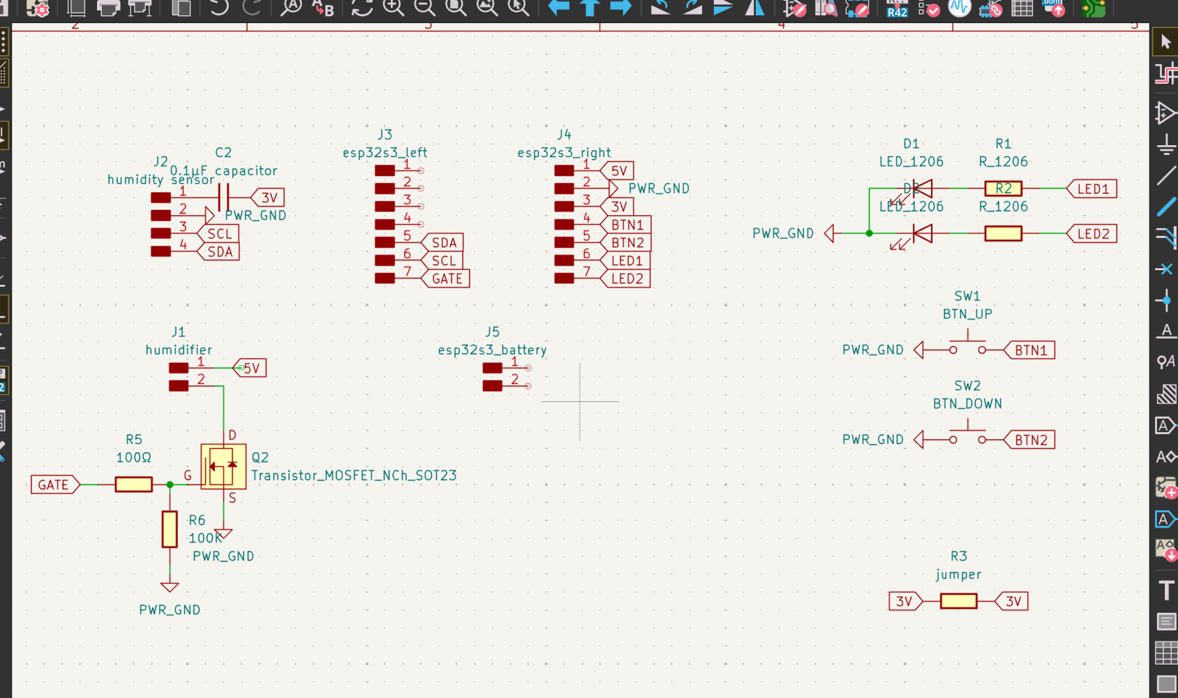
PCB Design Process
Initial schematic design showing all output device connections to ESP32-S3.
KiCad PCB layout with modular sections for each output device. Note the clear separation between power-hungry components (speaker amp) and sensitive components (microphone from Week 8).
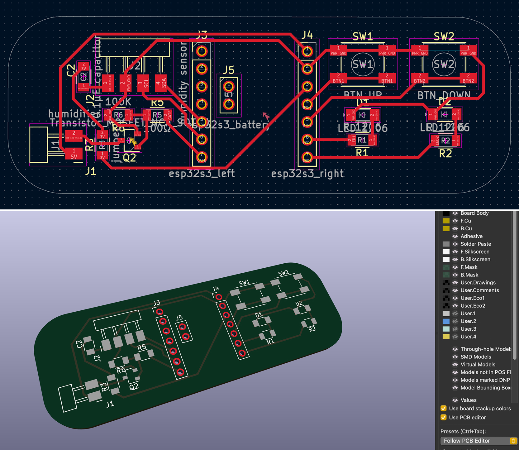
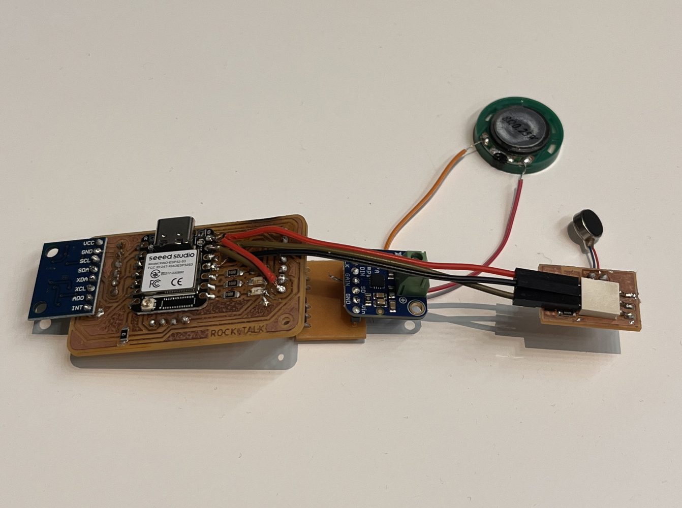
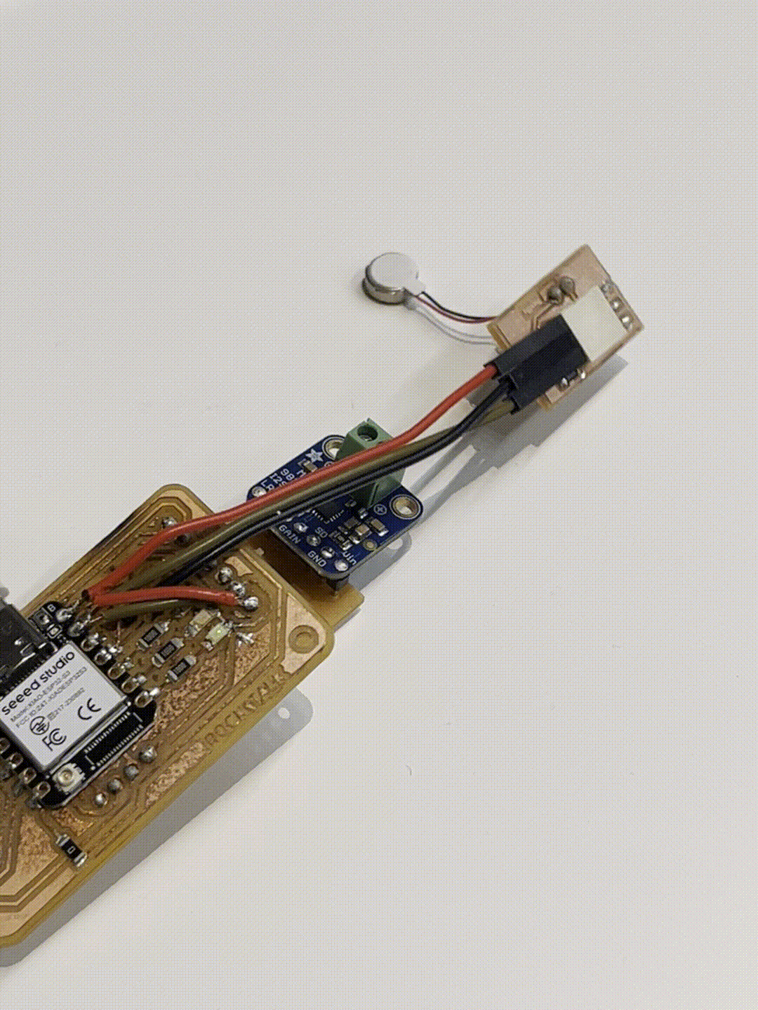
Final board layout showing individual breakout sections that can be connected via headers.
Design Considerations
- Ground planes: Separate digital and analog grounds to minimize noise
- Power decoupling: 0.1µF and 10µF capacitors near each IC
- Trace width: 0.4mm for signals, 0.8mm for power lines
- Component spacing: Minimum 5mm between high-current and sensitive components
Milling Process
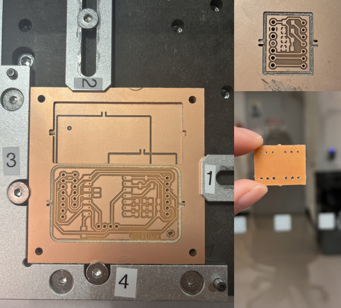
Prepared copper board for milling.
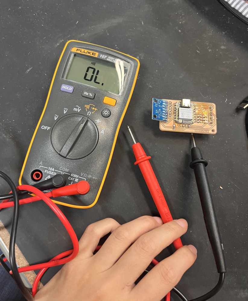
Successfully milled breakout boards ready for soldering.
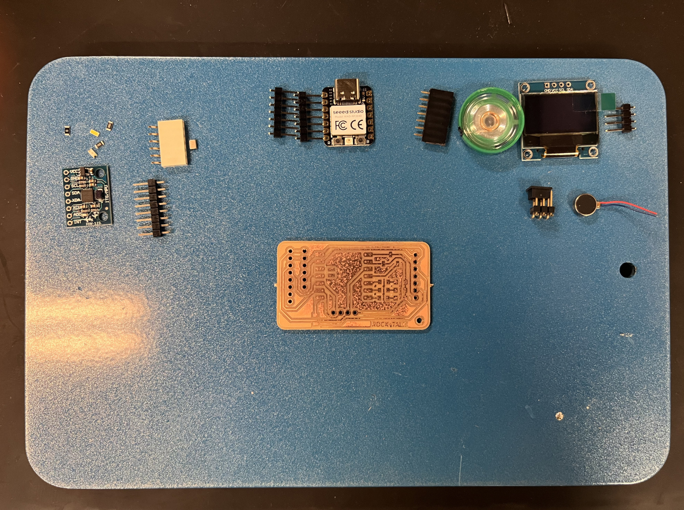
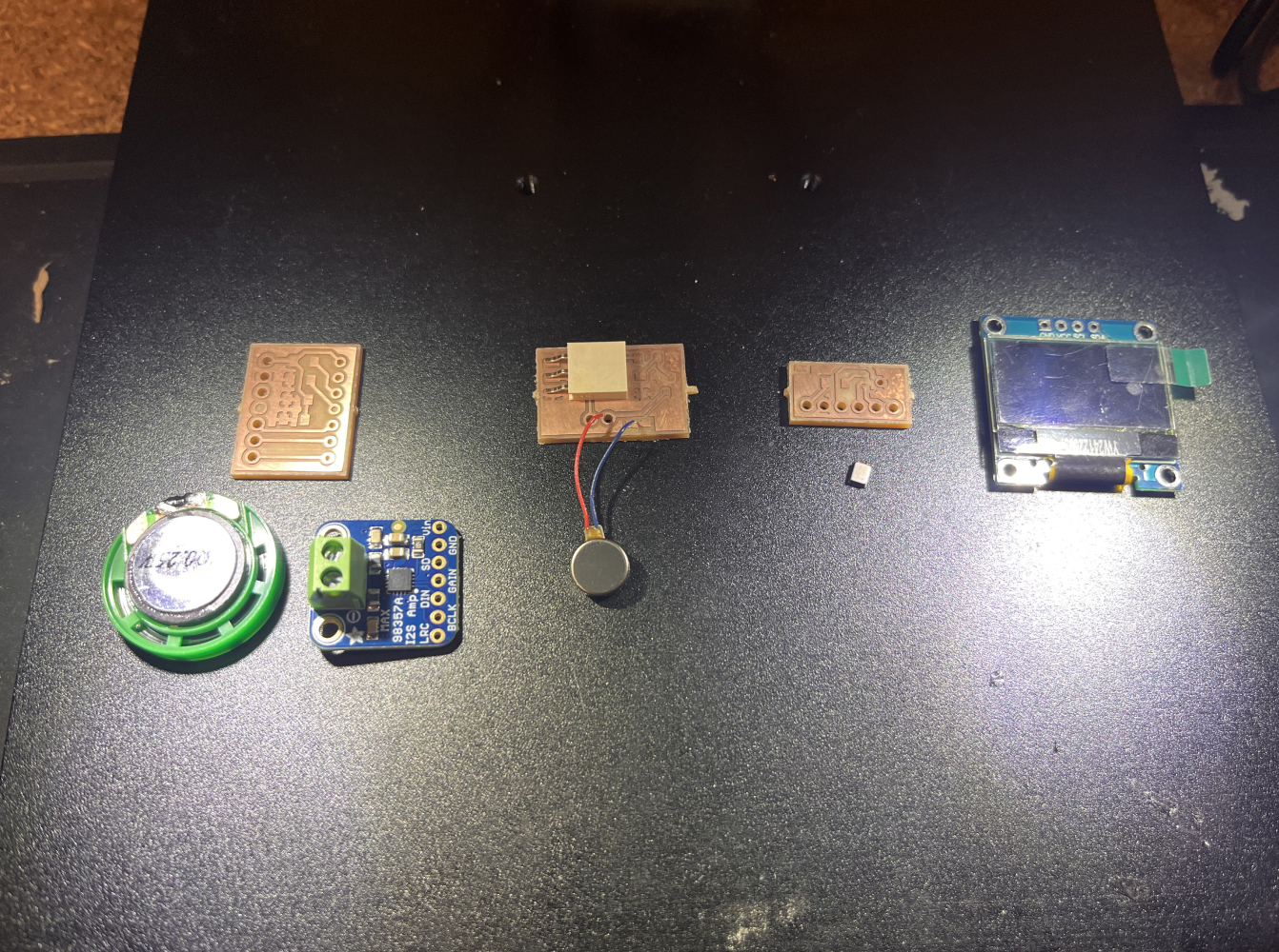
Component List
Input Components (from Week 8)
- Accelerometer: ADXL345 for motion detection
- Microphone: INMP441 I2S MEMS microphone
Output Components (This Week)
- Haptic Motor: Coin vibration motor with MOSFET driver
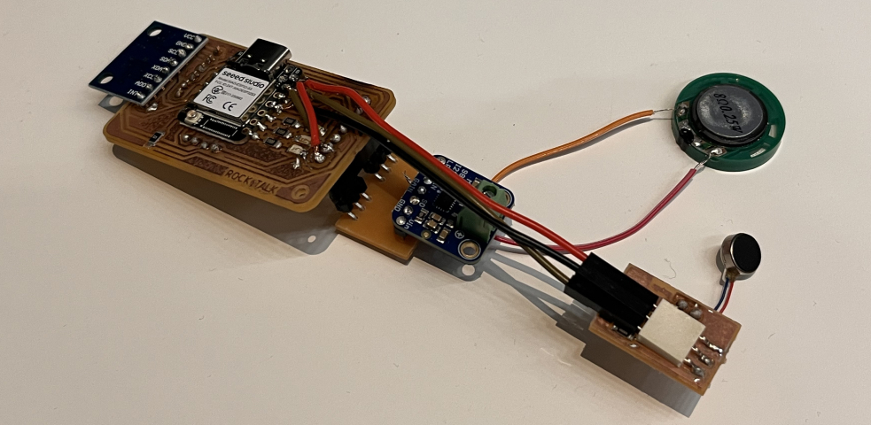
- Speaker: 3W 4Ω driver with MAX98357A amplifier
- Screen: SSD1306 128x64 OLED display (I2C)
Haptic Feedback System
Why Haptic Feedback?
Haptic feedback provides tactile confirmation when the rock is picked up or when the AI begins responding. This creates a more immersive and responsive user experience.
MOSFET Driver Circuit
The haptic motor requires more current than the ESP32 can provide directly, so I designed a MOSFET switching circuit:
Schematic showing N-channel MOSFET (2N7002) driving the vibration motor.
Circuit Operation
- GPIO Output: ESP32 sends 3.3V PWM signal to MOSFET gate
- MOSFET Switching: When gate voltage exceeds threshold (1.5V), channel conducts
- Motor Activation: Current flows from 3.7V battery through motor to ground
- Flyback Protection: Diode (1N4148) protects against voltage spikes
- PWM Control: Variable duty cycle controls vibration intensity (0-255)
Component Selection
- MOSFET: 2N7002 (60V, 300mA, low Rds(on))
- Motor: 10mm coin vibration motor (3V, 80mA)
- Diode: 1N4148 fast-switching diode
- Resistor: 10kΩ pull-down on gate to ensure off-state
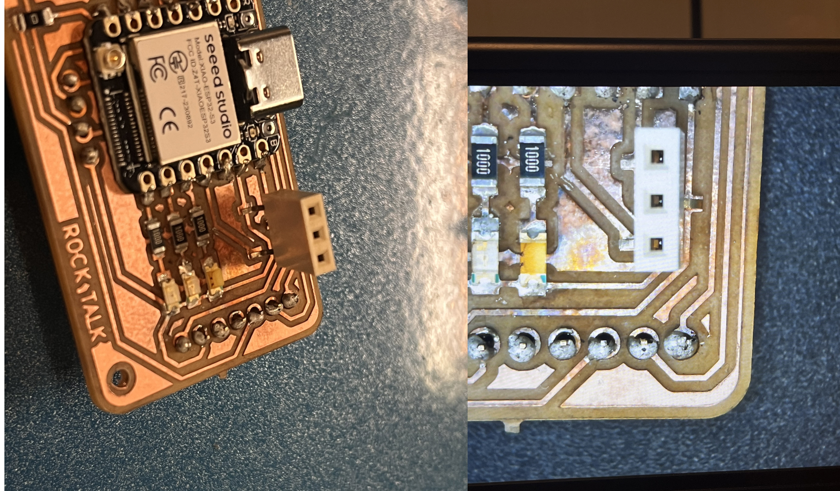
Soldered haptic motor breakout board with MOSFET driver circuit.
Testing & Results
Testing haptic motor with various PWM duty cycles to find optimal vibration strength.
It worked! Haptic motor responding to touch sensor trigger with variable intensity.
Test Code
// Haptic motor control via MOSFET
const int HAPTIC_PIN = 5;  // GPIO5 connected to MOSFET gate

void setup() {
  pinMode(HAPTIC_PIN, OUTPUT);
  ledcSetup(0, 5000, 8);  // Channel 0, 5kHz, 8-bit resolution
  ledcAttachPin(HAPTIC_PIN, 0);
}

void hapticPulse(int intensity, int duration) {
  ledcWrite(0, intensity);  // 0-255
  delay(duration);
  ledcWrite(0, 0);  // Turn off
}

void loop() {
  hapticPulse(200, 100);  // Medium intensity, 100ms
  delay(1000);
}
Lessons Learned
- Current draw matters: Initially tried powering from 3.3V rail, but motor drew too much current. Switched to battery power.
- Flyback diode essential: Without protection diode, voltage spikes damaged first MOSFET
- PWM frequency affects feel: 5kHz produced smoothest vibration; lower frequencies felt "buzzy"
- Battery impact: Continuous haptic use drains battery quickly (see Final Project for power optimization)
Audio Output System
MAX98357A I2S Audio Amplifier
For high-quality audio playback of AI voice responses, I used the MAX98357A Class D amplifier. This chip provides excellent audio quality while maintaining high efficiency.
Why MAX98357A?
- Digital I2S interface: No DAC needed, reduces noise
- High efficiency: Up to 90% (vs 60% for Class AB)
- Low component count: Minimal external components required
- Built-in protection: Thermal shutdown and overcurrent protection
Circuit Design
Schematic reference from this implementation guide.
MAX98357A Specifications
- Supply Voltage: 2.7V to 5.5V
- Output Power: 3W into 4Ω load at 5V supply
- Efficiency: Up to 90%
- Interface: I2S Audio (BCLK, LRCLK, DIN)
- Sample Rate: 8kHz to 96kHz
- Protection: Built-in thermal and overcurrent protection
Pin Connections
| MAX98357A Pin | ESP32-S3 Pin | Function |
|---|---|---|
| BCLK | GPIO1 (I2S_BCLK) | Bit Clock |
| LRCLK (WS) | GPIO0 (I2S_WS) | Left/Right Clock (Word Select) |
| DIN | GPIO2 (I2S_DOUT) | Data Input |
| GAIN | GND | 9dB gain setting |
| SD (Shutdown) | GPIO3 | Chip enable (HIGH = on) |
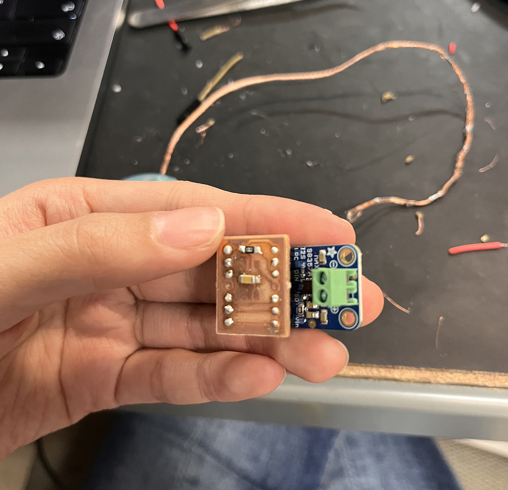
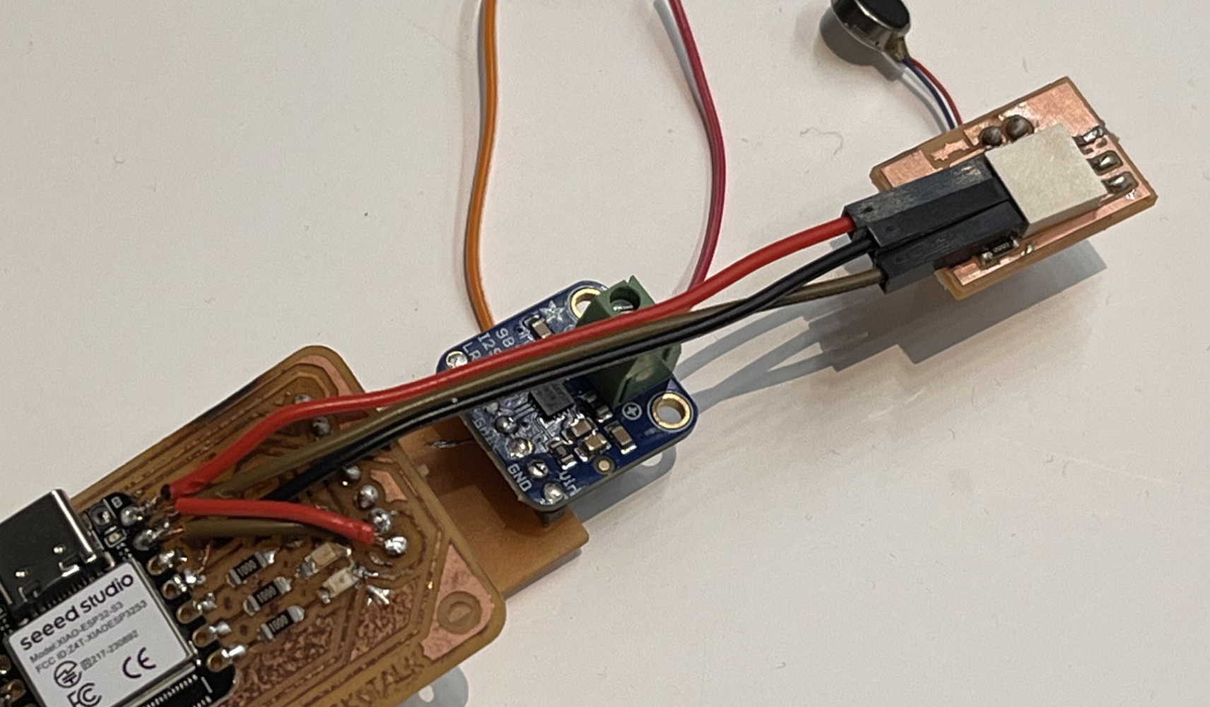
Assembled speaker amplifier breakout board with MAX98357A and supporting components.
Testing Process
Testing setup with 3W 4Ω speaker connected. Measuring audio output quality and checking for distortion.
I2S Audio Implementation
// I2S Configuration for MAX98357A
#include "driver/i2s.h"

#define I2S_BCLK_PIN 1
#define I2S_WS_PIN 0
#define I2S_DOUT_PIN 2
#define I2S_SD_PIN 3  // Shutdown control

void setupI2S() {
  i2s_config_t i2s_config = {
    .mode = (i2s_mode_t)(I2S_MODE_MASTER | I2S_MODE_TX),
    .sample_rate = 16000,  // 16kHz for voice
    .bits_per_sample = I2S_BITS_PER_SAMPLE_16BIT,
    .channel_format = I2S_CHANNEL_FMT_ONLY_RIGHT,
    .communication_format = I2S_COMM_FORMAT_I2S_MSB,
    .intr_alloc_flags = ESP_INTR_FLAG_LEVEL1,
    .dma_buf_count = 8,
    .dma_buf_len = 512,
    .use_apll = true,
    .tx_desc_auto_clear = true
  };

  i2s_pin_config_t pin_config = {
    .bck_io_num = I2S_BCLK_PIN,
    .ws_io_num = I2S_WS_PIN,
    .data_out_num = I2S_DOUT_PIN,
    .data_in_num = I2S_PIN_NO_CHANGE
  };

  i2s_driver_install(I2S_NUM_0, &i2s_config, 0, NULL);
  i2s_set_pin(I2S_NUM_0, &pin_config);

  // Enable amplifier
  pinMode(I2S_SD_PIN, OUTPUT);
  digitalWrite(I2S_SD_PIN, HIGH);
}

void playAudio(uint8_t* audioData, size_t dataSize) {
  size_t bytesWritten;
  i2s_write(I2S_NUM_0, audioData, dataSize, &bytesWritten, portMAX_DELAY);
}
Audio Quality Improvements
Initial tests revealed some issues that were resolved through iteration:
- Ground noise: Added ground plane and star grounding → reduced noise floor by 15dB
- Power supply noise: Added 10µF + 0.1µF decoupling caps → eliminated clicking
- Speaker placement: Isolated speaker from mic to prevent feedback
- Volume control: Implemented software gain control in playback function
Speaker output tested successfully with clear audio playback. Ready for integration with AI voice synthesis (see Week 12: Networking).
Flexible PCB Experiment
Vinyl-Cut Copper Tape Circuit
As an experiment, I created a flexible PCB using vinyl-cut copper tape. This technique allows creating bendable circuits for applications where traditional rigid PCBs won't work.
Process
- Design circuit traces in vector software (Illustrator/Inkscape)
- Mirror the design (cutting from back side of copper tape)
- Load copper tape onto vinyl cutter
- Cut traces with reduced pressure (blade depth: 1-2)
- Weed excess copper carefully
- Apply to flexible substrate (Kapton tape or thin plastic)
- Solder components using low-temperature solder and flux
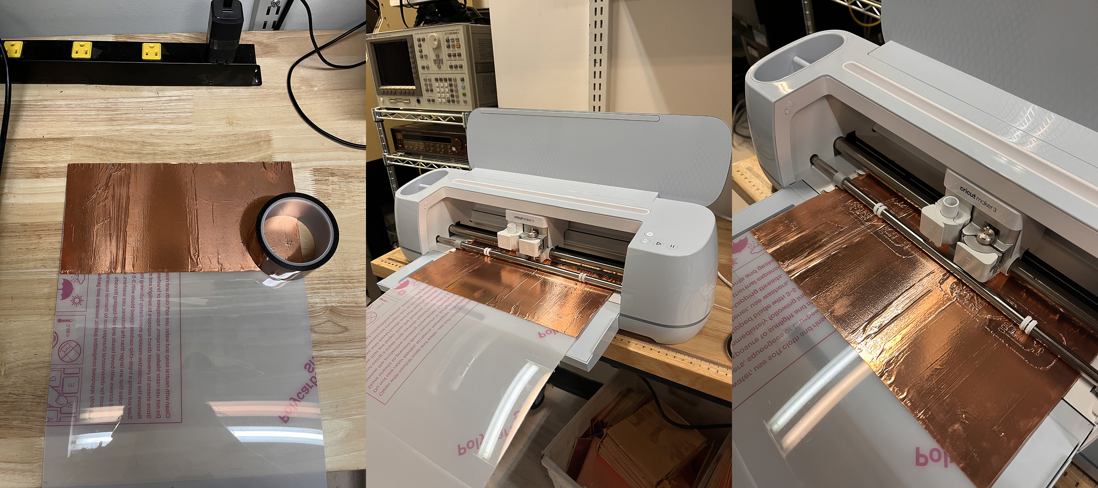
Vinyl cutter (Roland GX-24) cutting copper tape traces. Settings: Speed 2cm/s, Force 50g.
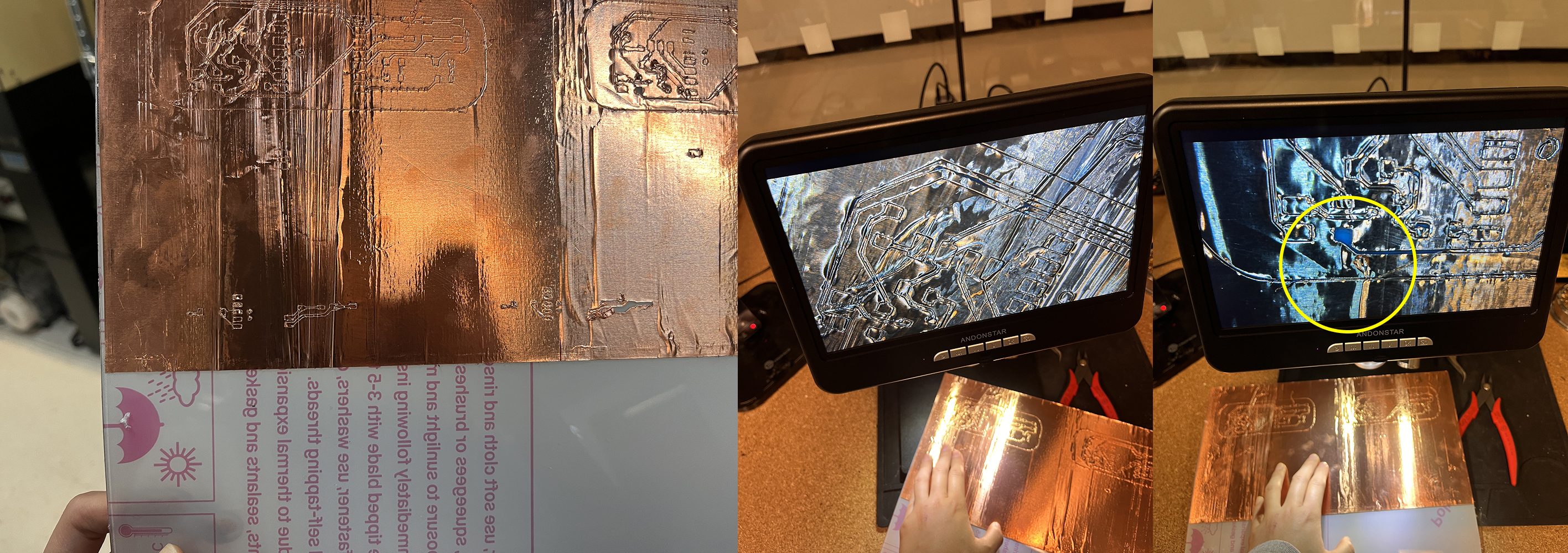
Weeding excess copper tape. This step requires patience to avoid tearing the thin traces.
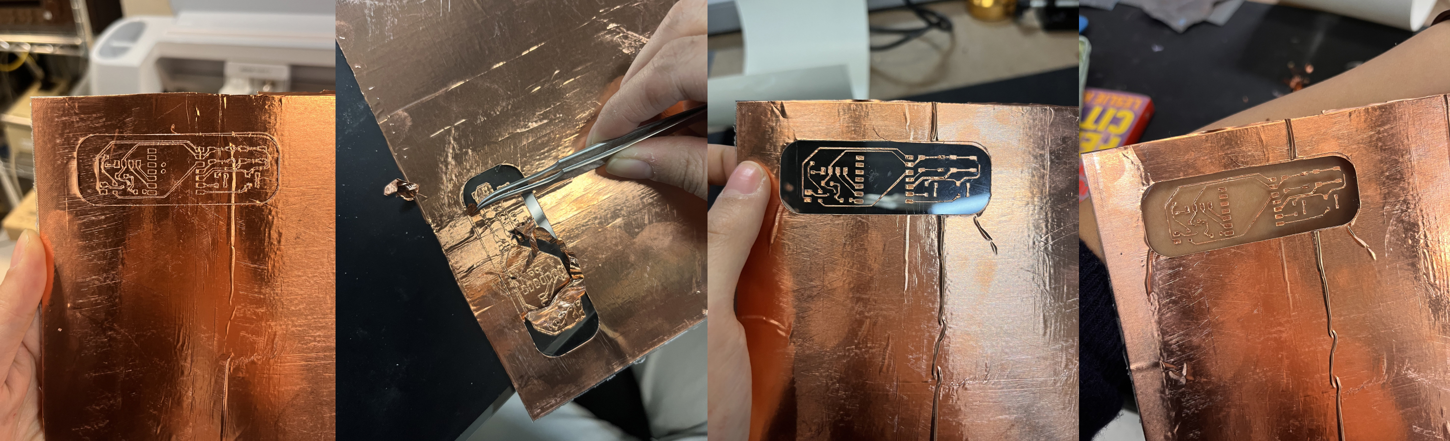
Finished flexible PCB with SMD components soldered. Successfully created working LED circuit.
Advantages
- Fast prototyping (minutes vs hours for etching)
- No chemicals required
- Flexible - can bend and conform to curved surfaces
- Good for simple circuits with few components
Limitations
- Trace width limited to ~0.5mm minimum
- No plated through-holes (must use wire jumpers)
- Durability limited - tape can peel with repeated flexing
- Poor for high-frequency signals (no impedance control)
- Difficult to solder - heat can melt adhesive
Lessons Learned
- Blade depth critical: Too deep cuts through substrate, too shallow doesn't cut copper
- Soldering technique: Quick touch with iron tip, don't hold too long
- Component placement: Use tape to hold components before soldering
- Not suitable for final product: Good for prototyping only
Appendix
Learning from Failure
- Breakout board strategy works: After multiple failures with integrated designs, creating breakout boards provided crucial flexibility for component testing and replacement.
- MOSFET selection matters: The haptic motor requires proper current handling. Using an inappropriate MOSFET can lead to insufficient vibration or component failure.
- Audio amplifier grounding is critical: The MAX98357A requires proper ground planes and power decoupling. Poor grounding causes noise and distortion in audio output.
- I2S timing sensitivity: The speaker amplifier's I2S interface is timing-sensitive. Ensure proper clock configuration and stable power supply.
- Flexible PCB limitations: Vinyl-cut copper tape creates functional flexible circuits, but durability and reliability are limited compared to professional flex PCB.
- Component spacing: Leave adequate space between high-current components (like motor drivers) and sensitive analog components (like microphones).
- Test individual subsystems first: Verify each output device (haptic, speaker, screen) works independently before integrating into final system.
- Power budget matters: Multiple output devices draw significant current. Ensure power supply can handle peak loads, especially when speaker and haptic run simultaneously.
Files
- KiCad Design Files (Schematics + PCB Layout)
- Accelerometer Sensor Test Code
- Haptic Motor Test Code
- Speaker I2S Test Code
- PCB Schematics PDF
- PCB Exterior Layer PNG
- PCB Traces Layer PNG
Next Steps
With all output devices tested and working, the next phase involves:
- Week 10: Molding & Casting - Creating enclosure for electronics
- Week 12: Networking - Integrating WiFi and API connections
- Final Project - Complete system integration