SmartPi Embedded Controller Design
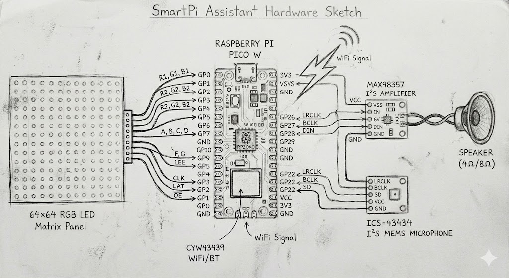
The SmartPi Assistant is an embedded interactive device built around the Raspberry Pi Pico W microcontroller. It integrates a 64×64 LED matrix panel as the primary visual display, a 3–4 Ω speaker for audio output, and an Adafruit MAX98357 amplifier to drive the speaker with clear sound. The design also accommodates an Adafruit ICS-43434 digital I²S MEMS microphone for capturing voice commands, enabling natural, voice-based interaction.
Why Raspberry Pi Pico W?
The Raspberry Pi Pico W is an ideal choice for the SmartPi Embedded Controller because it combines affordability, performance, and built-in wireless connectivity in a compact form factor. Powered by the RP2040 dual-core ARM Cortex-M0+ processor, it provides sufficient computational power for real-time sensor data acquisition, control logic, and lightweight edge AI tasks, while maintaining low power consumption—critical for continuous operation.
Display Interface: HUB75 LED Matrix Connection
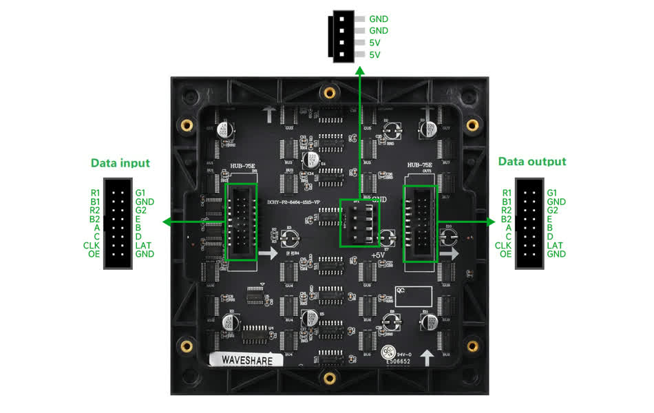
The HUB75 (2×8) connector serves as the standard interface between the Raspberry Pi Pico W and the 64×64 RGB LED matrix panel. It provides a set of 16 data and control lines, including color data inputs (R, G, B), row address lines, latch, clock, and output enable signals, which together allow precise control of the timing and brightness of individual LEDs.
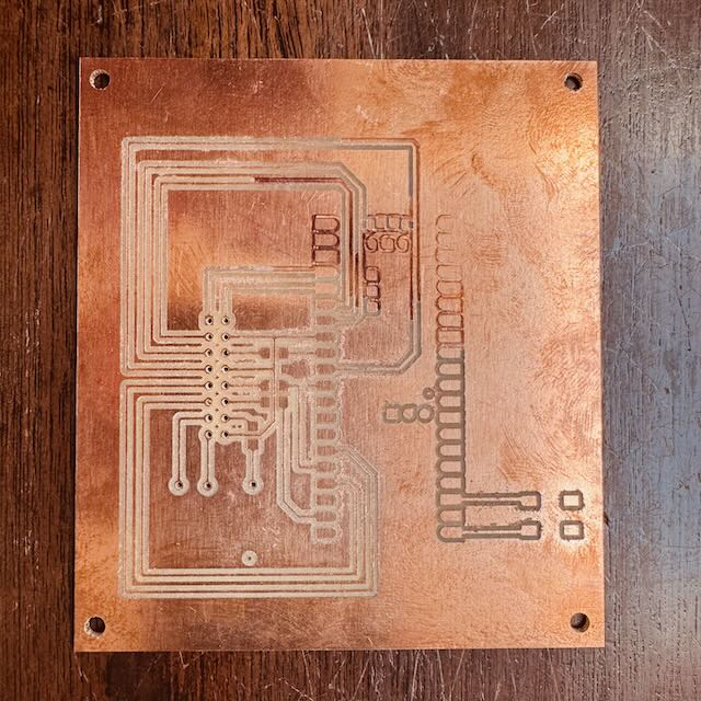
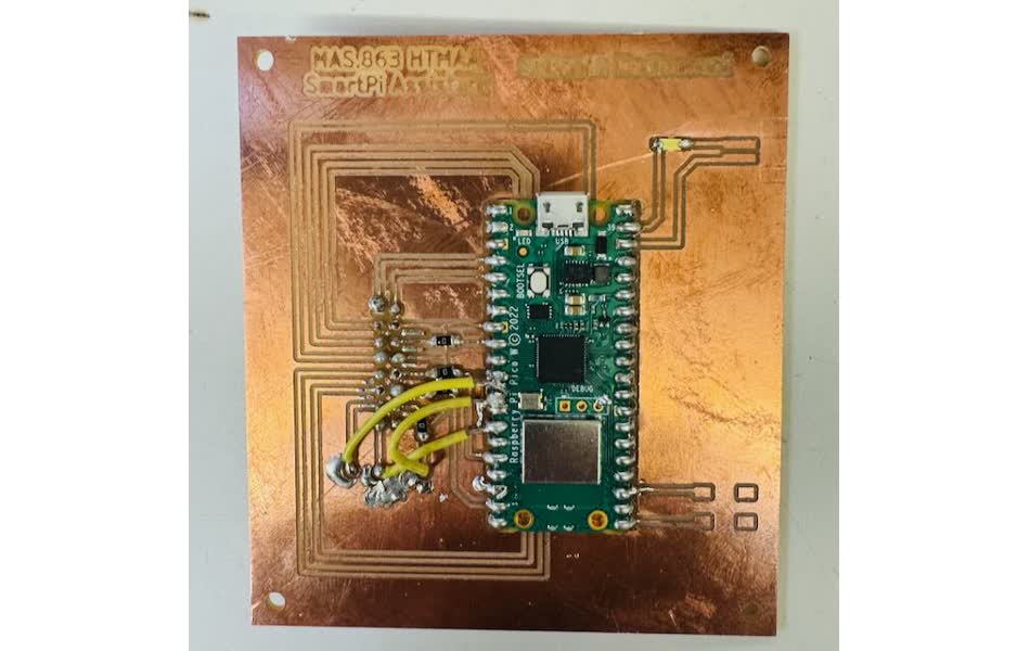
Hardware Implementation: First Prototype
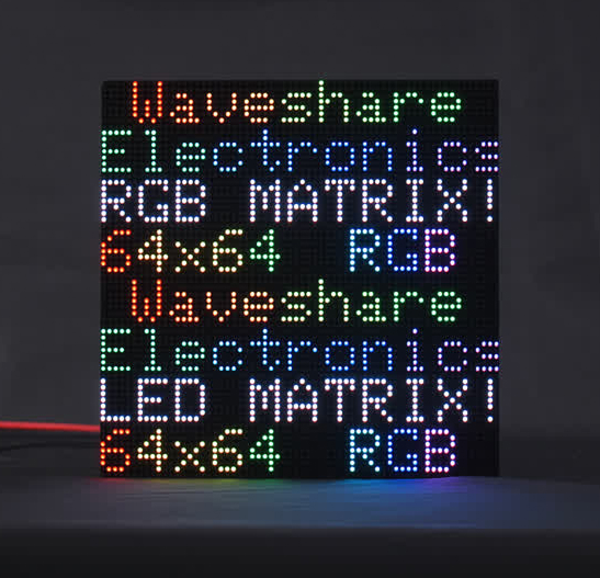
- I procured a 64×64 full-color LED matrix panel with 2mm pitch from Waveshare.com. These are modular pieces that can be daisy chained together to create larger LED matrices.
- I designed a PCB board to interface the LED matrix panel with Raspberry Pi Pico W using the HUB75 standard socket
- Created the traces in the layout view
There were some crossover issues after the manual trace layout, so I dealt with a couple of crossovers using zero ohm resistors as bridges. There were 3 more crossovers to handle. Instead of opting for a 2-sided board (and the more involved milling process), I discussed with Anthony and came up with making 3 holes through which we'd run wires to connect the HUB75 CLK, LAT, and OE pins from the back of the board, using header pins on the Raspberry Pi Pico.
Added a JST connector for power and a switch to turn the device on/off.
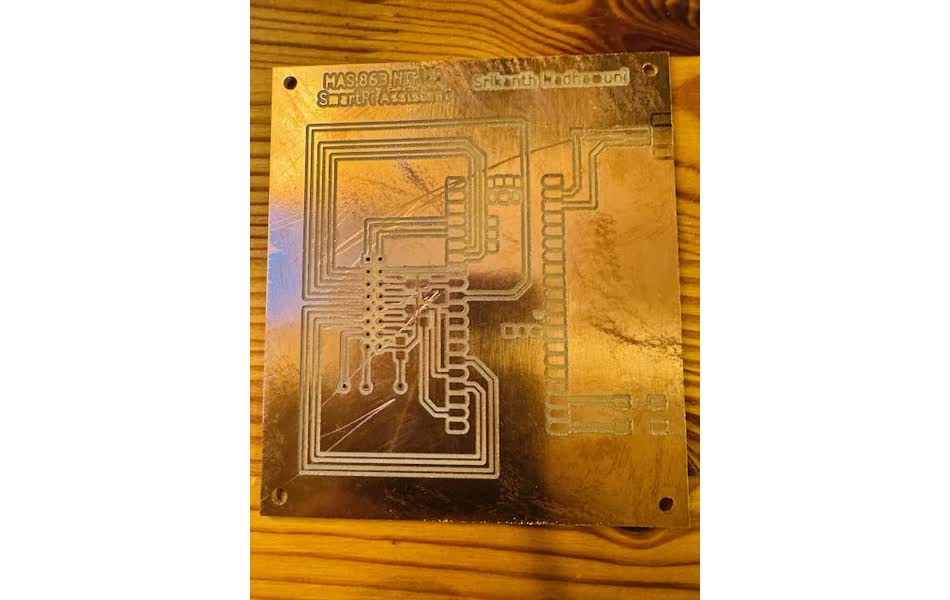
PCB Fabrication Process
- Created an Eagle 9.x compatible board file (.brd extension) from AutoCAD Fusion
- Loaded the .brd file into the Bantam software connected to the OtherMill milling machine
- Taped a single-sided board using double-sided tape, ensuring no overlaps (which would mess up the milling if the board is uneven)
- Loaded the 1/64" mill bit and started milling the .brd file
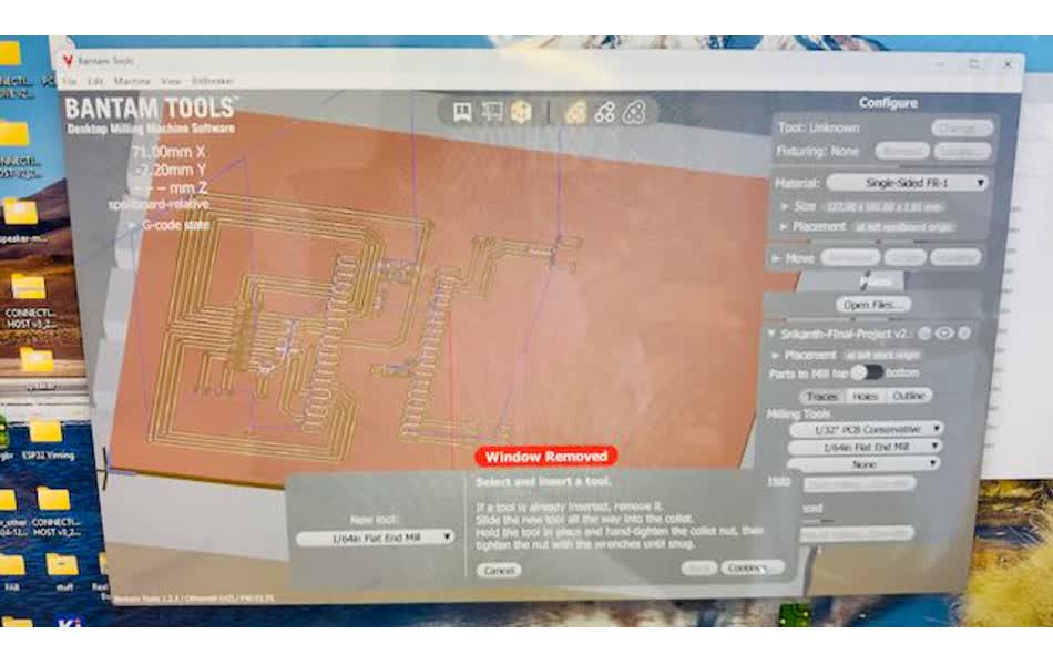
- Clicked "Mill All Visible" with the 1/64" mill bit to mill the finer portions
- After fine milling, loaded the 1/32" larger mill bit for fast milling of larger areas
- After completing all traces, used the 1/32" mill bit to drill holes and cut the outline
- After all this, discovered the board was incomplete—missing the right side Raspberry Pi Pico pins, power points, and the course name text!
- Anthony exported a .gerber file and loaded its constituent parts for the trace, holes, and outline, and restarted the job
- This time the milling machine completed the entire board with all pins, traces, holes, outline, and importantly the text with the course and my name on it
Assembly and Soldering
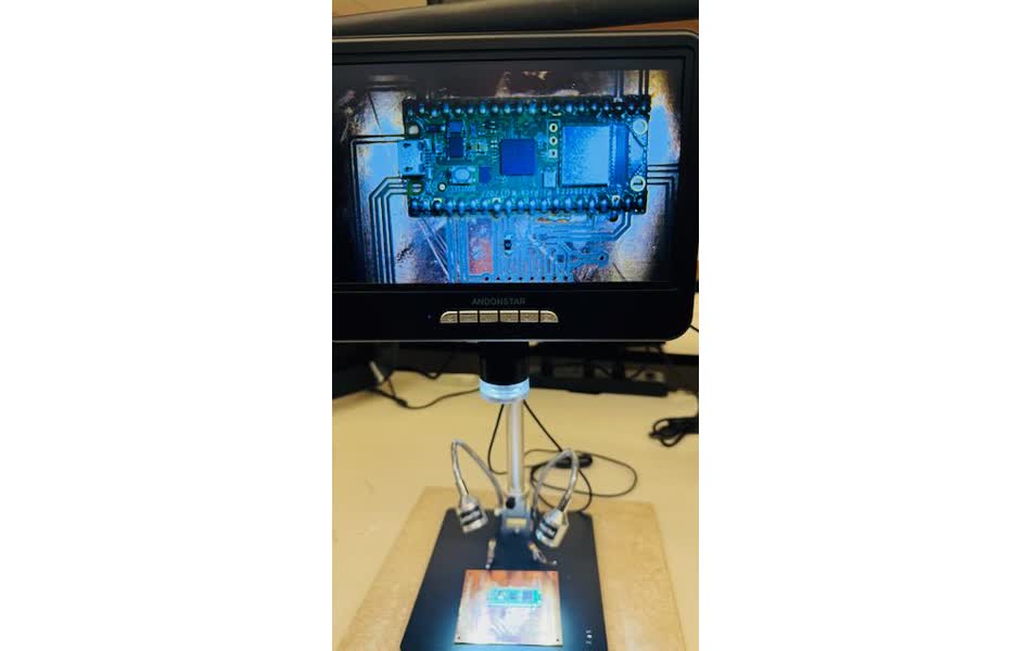
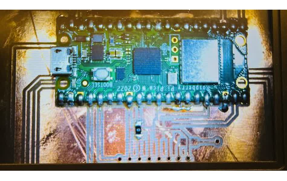
- Started soldering the Raspberry Pi Pico W onto the newly milled PCB. The Adonstar digital magnifier was super useful for precise placement, ensuring the tiny copper pads were centered correctly.
- Cleaned my soldering iron with a small amount of solder to get good flow, then put a blob of solder on the bottom left pin. Holding the RP Pico W down, I applied the soldering iron and got one pin securely fastened. After that, it was just a matter of completing the rest.
The digital magnifier was not actually useful for soldering itself—it helped more to inspect the solders and ensure there were no bridges between pins.
- Proceeded to solder the zero ohm resistors, which were super tiny and difficult to keep in place. They would move as the soldering iron approached, getting soldered at weird angles. Heating the trace pad again and ever so slightly moving them back into place was challenging. Got all 3 zero-ohm resistors soldered to bridge underlying traces and tested connectivity—all was fine.
- Finally soldered the diode from the external 5V Vcc point to VSYS (pin 39), ensuring the tiny (barely visible) arrow mark was in the correct direction. Added the 3 wires needed to avoid trace crossover challenges.
Lessons Learned: PCB Design Mistakes
Despite careful planning, several critical mistakes emerged during the PCB fabrication and assembly process. These errors provided valuable learning experiences about PCB design considerations.
1. Inverted HUB75 Connector Placement
Since I didn't have a female HUB75 connector component in the lab, I had to make the HUB75 connector using header pins. Due to the single-sided PCB board, I was forced to solder the header pins on the milled side, with pins sticking out at the bottom. This resulted in wrong (inverted) connections to the display matrix.
2. Missing Power Supply for LED Matrix
The LED matrix needs a 5V power supply with high current capacity. I made no provisions to drive the display board besides powering the Raspberry Pi Pico W itself—a rookie mistake. A 64×64 RGB LED matrix can draw several amps.
3. Poor USB Connector Accessibility
By placing the Raspberry Pi Pico W in the middle of the PCB board, I made it hard to insert the micro USB port. The board should have been designed with the RP Pico at the top edge for easy access.
Key Takeaways
- Connector orientation matters: Verify that through-hole connectors will mate correctly with their counterpart cables
- Power budget planning: Calculate maximum current draw early and provision adequate power supply connections
- Physical accessibility: Place connectors and buttons near board edges
Derisking the Project with temporary Adapter Board
I needed to go to India for 10 days for a meeting and event. I knew the PCB still had power connections and switch to be connected and the HUB75 pins to be tested. It was unlikely all this was going to work in a day. There was also learning the software environment and developing software to test the LED matrix board.
I decided to de-risk the project by using a pre-fabricated RGB Matrix Adapter Board, which I had bought when I ordered the Matrix Board itself. This was a life saver.
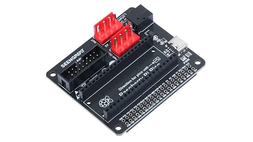
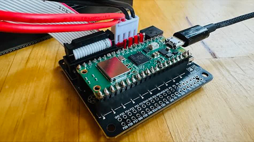
- Soldered header pins to the Raspberry Pi Pico so it could readily fit into the adapter board
- Pushed the RP Pico W with header pins into the adapter board and connected the HUB75 ribbon connector and power supply JST connector
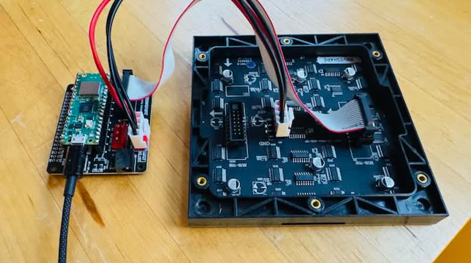
- Connected the adapter card to the RGB Matrix
- Connected the micro USB cable to the Raspberry Pi Pico and the other end to my MacBook
Setting up CircuitPython Environment
I decided to use CircuitPython on the RP Pico with the Mu Editor. Setup instructions:
- Downloaded the CircuitPython UF2 file
- Held down the BOOTSEL button, then plugged the Pico into a USB port
- Released the BOOTSEL button after connecting. It installed as "RPI-RP2"
- Dragged and dropped the CircuitPython UF2 file onto "RPI-RP2" volume
- The Pico rebooted, a new disk drive "CIRCUITPY" appeared—done flashing
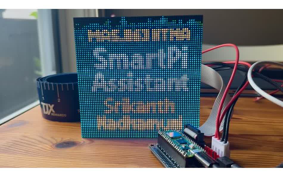
Initial Test Program
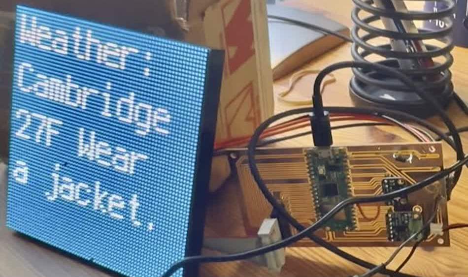
This CircuitPython test program initializes a 64×64 HUB75 RGB LED matrix connected to a Raspberry Pi Pico W using the specified GPIO pin mapping. It creates a full-screen bitmap with a single palette color and repeatedly cycles that color through red, green, blue, white, and black. This verifies that the panel wiring, color channels, and basic timing/refresh are all working correctly.
import board
import displayio
import framebufferio
import rgbmatrix
import time

displayio.release_displays()

# HUB75 + Seengreat Pico adapter pin map
rgb_pins = [board.GP2, board.GP3, board.GP4,
            board.GP5, board.GP8, board.GP9]
addr_pins = [board.GP10, board.GP16, board.GP18, board.GP20, board.GP22]
clock_pin = board.GP11
latch_pin = board.GP12
oe_pin = board.GP13

WIDTH = 64
HEIGHT = 64

matrix = rgbmatrix.RGBMatrix(
    width=WIDTH, height=HEIGHT, bit_depth=5,
    rgb_pins=rgb_pins, addr_pins=addr_pins,
    clock_pin=clock_pin, latch_pin=latch_pin,
    output_enable_pin=oe_pin,
    tile=1, serpentine=False, doublebuffer=True
)

display = framebufferio.FramebufferDisplay(matrix, auto_refresh=True)

palette = displayio.Palette(1)
bitmap = displayio.Bitmap(WIDTH, HEIGHT, 1)
tg = displayio.TileGrid(bitmap, pixel_shader=palette)
group = displayio.Group()
group.append(tg)
display.root_group = group

def fill(rgb_hex):
    palette[0] = rgb_hex
    time.sleep(0.5)

while True:
    fill(0xFF0000)  # red
    fill(0x00FF00)  # green
    fill(0x0000FF)  # blue
    fill(0xFFFFFF)  # white
    fill(0x000000)  # black
The test program worked!
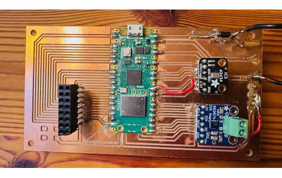
Adding Voice Interaction Capabilities
Following insights from the MAS.863 classes on input and output devices, I recognized an opportunity to enhance the SmartPi by adding bidirectional audio capabilities. While the initial design focused solely on visual output through the LED matrix, the addition of audio I/O transforms the device into a truly interactive assistant.
This enhancement enables:
- Audio Output (Speaker): Vocalize displayed messages for situations where visual attention isn't possible
- Audio Input (Microphone): Voice input shifts SmartPi from passive display to interactive assistant supporting a "pull" model
I chose to implement a fully digital audio path using the I²S (Inter-IC Sound) protocol. This eliminates the need for external ADC/DAC converters, reduces noise, simplifies PCB routing, and ensures bit-perfect audio transmission.
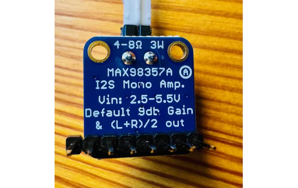
Audio Output: Adafruit MAX98357 I²S Amplifier
The Adafruit MAX98357 is a digital-to-analog Class-D audio amplifier that converts I²S digital audio into high-quality analog sound capable of driving a speaker directly. The Raspberry Pi Pico W lacks both a DAC and sufficient output power for a low-impedance speaker. The MAX98357 fills this gap by delivering up to 3 watts of power to a 3–4 Ω speaker.
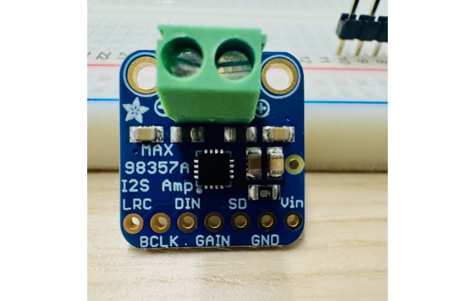
MAX98357 Connection to Raspberry Pi Pico W
| MAX98357 Pin | Connect to Pico W | Notes |
|---|---|---|
| VIN | VSYS (5V) | Power supply 2.5V–5.5V. At 5V can deliver up to 3W into 4Ω speaker |
| GND | GND | Common ground with Pico |
| SD | GP16 | Shutdown/Mode pin. Controls stereo mode and shutdown |
| GAIN | GP17 | Sets amplifier gain. Default 9dB (floating) |
| DIN | GP18 | I²S Data In - receives digital audio data |
| BCLK | GP19 | I²S Bit Clock - timing signal |
| LRCLK | GP20 | I²S Left/Right Clock (Word Select) |
Audio Input: Adafruit ICS-43434 I²S MEMS Microphone
The Adafruit ICS-43434 is a digital I²S MEMS microphone that captures high-quality audio and outputs it as a clean, noise-free digital signal. Unlike analog microphones requiring external amplification, the ICS-43434 performs analog-to-digital conversion internally and transmits audio data directly to the Pico W over I²S.
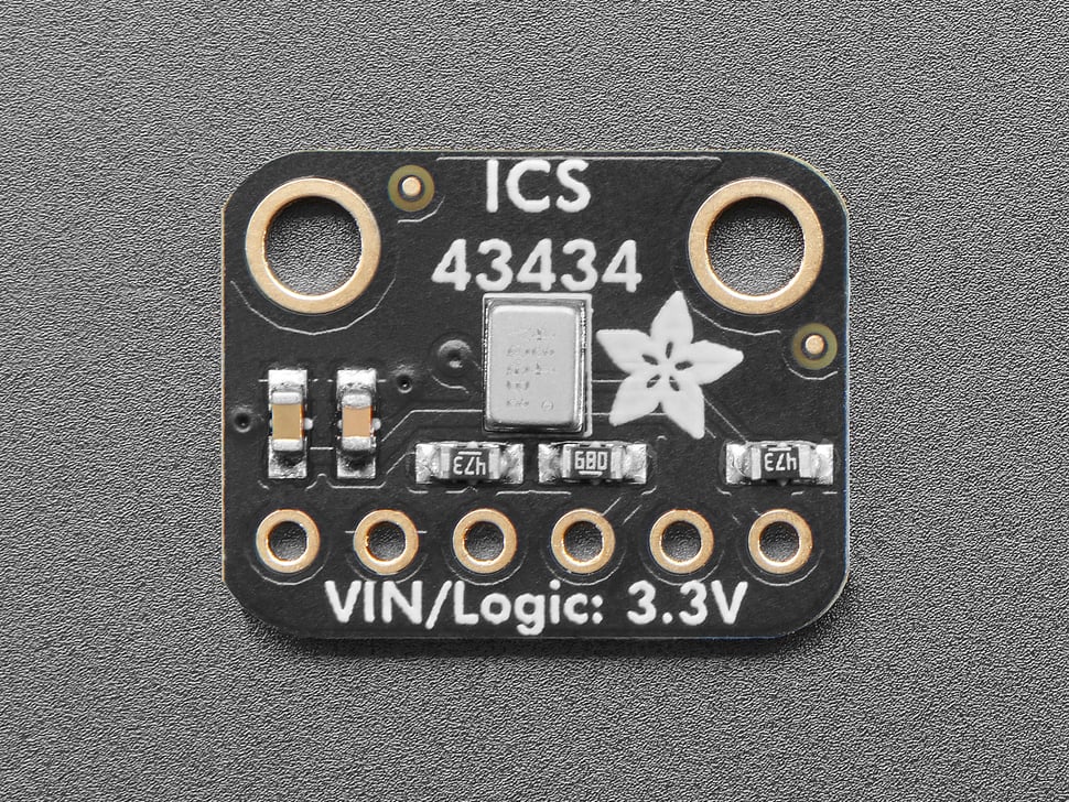
ICS-43434 Connection to Raspberry Pi Pico W
| ICS-43434 Pin | Connect to Pico W | Pico Pin # | Notes |
|---|---|---|---|
| 3V3 (VDD) | 3V3(OUT) | 36 | Power supply 1.6V to 3.6V. Use 3.3V |
| GND | GND | 28 | Power and data ground |
| WS (LRCLK) | GP22 | 29 | Left/Right Clock (Word Select) |
| SCK (BCLK) | GP26 | 31 | Bit Clock (data clock) - 2-4 MHz |
| SD (DOUT) | GP27 | 32 | Data Output from the mic |
| SEL | GP28 | 34 | Channel select. Low = left channel (mono) |
PCB Version 3: Final Production Design
Building upon lessons from previous iterations, PCB V3 represents the final production-ready design with all components integrated, proper power distribution, and optimized routing.
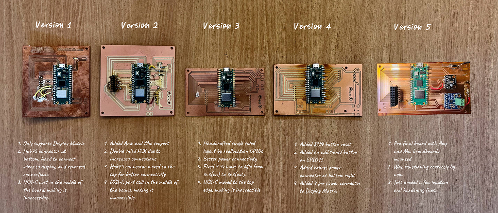
Key Improvements
- Proper HUB75 connector orientation: Female connector mounted correctly
- Dedicated 5V power supply: Separate power input for LED matrix (up to 4A capacity)
- Improved component placement: Pico W at edge for easy USB access
- Integrated audio subsystem: Both MAX98357 and ICS-43434 on-board
- Two-layer design: Proper via routing eliminates wire jumpers
Conclusion
The SmartPi hardware development journey demonstrates the iterative nature of embedded systems design. From the initial single-sided PCB with manual wire jumpers to the final two-layer production board with integrated audio, each iteration addressed specific design flaws and added new capabilities.
Key Achievements
- ✅ Successfully interfaced 64×64 RGB LED matrix via HUB75 protocol
- ✅ Integrated digital I²S audio input and output
- ✅ Designed and fabricated three PCB iterations with progressive improvements
- ✅ Achieved reliable wireless connectivity via Pico W's built-in WiFi
- ✅ Created production-ready hardware platform for ambient intelligence
The final hardware platform provides a solid foundation for the SmartPi Assistant, combining visual display, audio I/O, and wireless connectivity in a compact, low-power package suitable for continuous operation as an ambient intelligence device.