Switching Power Supplies
With all that said, how could we get around the limitations of linear supplies? Poor efficiency + low max power output. Instead let’s use switching (FETs or BJTs), and filtering to step voltages down or up, without so many wasteful components.
Background
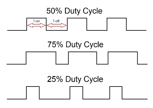
Duty Cycle
- We could imagine a 10V supply chopped at 50% duty cycle might start to look like a 5V supply if chopped at high enough frequencies. Note the distinction between switching frequency and duty cycle!
The Canonical Cell
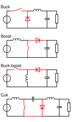
- Pretty sure this is sort of an antiquated term, but it refers to the recurring use of a switch, inductor, and capacitor. These components are at the core of the 4 primary switching power supplies we will discuss in the sections below (including the flyback which is not shown in the picture below). By just rearranging them we can accomplish everything we will discuss in the next section.
- Note that sometimes schematics will show the “switch” as a transistor and a diode (as shown in the pictures below), and sometimes they will show two transistors. Swapping the diode for a transistor is a matter of improving efficiency (no voltage drop across the diode), but introduces other challenges such as shoot-through (another point for half-bridge drivers).
Half Bridges
- The word “switch” used in the section above is an oversimplification.
- In reality we rarely leave loads floating (particularly if they’re inductive because of flyback) - we want to either supply them with current or ground them to discharge.
- To avoid worrying about timing (what happens if both transistors are on simultaneously?) as well as the complexity of driving high side transistors (what’s happening to the source voltage of the high side transistor while we switch), it’s common to use a dedicated IC to drive both high and low side FETs called a half bridge driver.
- As an example, here’s the infineon IR2104 Half Bridge Driver.
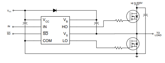
Note the gate drive resistors (remember that everything is an inductor and capacitor) + bucket capacitor tapping into high side source voltage + bypass capacitor. Why are these components here?
Characterizing Converter Performance
Three criteria are generally used to characterize the performance of a switched power supply
CCM vs. DCM - Is our inductor running out of current?
Current Ripple - How much steady state current fluctuation can our load tolerate?
Voltage Ripple - Same for output voltage (remember we
The equations below can be used to calculate these parameters for a buck converter, but see the first link for each converter for their specific equations. Think about changing switching frequency effects specs. Note that the inductor is driving our current ripple spec, and the cap is driving the voltage ripple spec.

Buck Converter
- Overview of buck converter design and component selection
- Good animation of a buck converter in operation
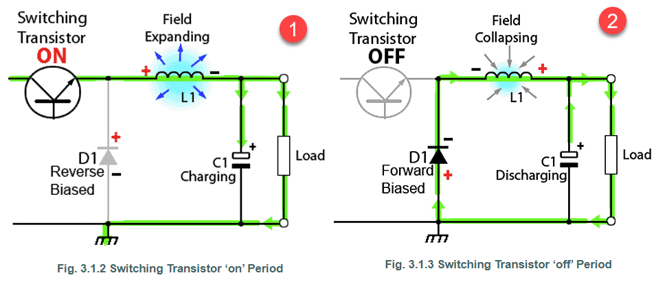

We can relate output voltage to input voltage as a proportion of duty cycle. At D = 1 V_out = V_in. At D = 0.5 V_out = V_in.
Why an inductor and a capacitor? Both are critical for storing energy and they work in tandem to minimize both voltage (capacitor) and current (inductor) ripple. See the equations for voltage and current ripple for a better understanding of why.
Boost Converter
- Overview of boost converter design and component selection
- Good animation of a boost converter in operation
- If we reverse the direction of our buck converter we create a boost converter. Now we will charge up an isolated inductor in series with the load, and then switch such that both the inductor and source voltage are applied simultaneously to charge the capacitor and load itself. Now those two voltages will sum and can increase
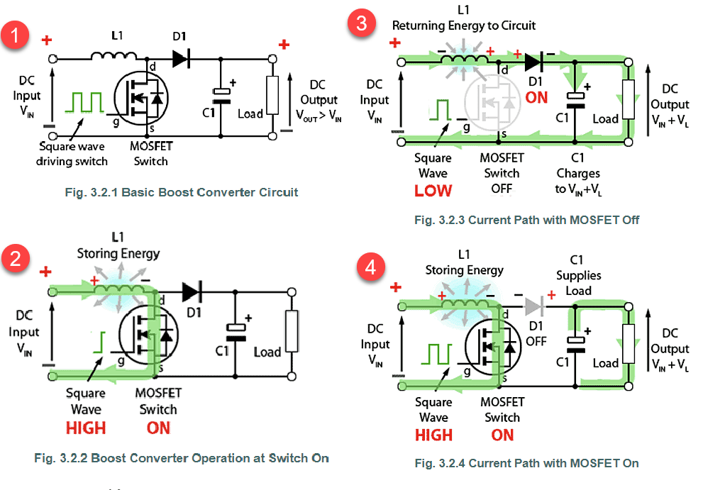

Again we can relate output voltage to input voltage. Let’s think about what happens at low duty cycles. For D = 0.1, V_out = 1.11 _ V_in. For D = 0.9 V_out = 10 _ V_in.
The above suggests that we could achieve infinitely high voltages as D approaches 1. In reality buck converters are not typically run at duty cycles greater than 80%.
Buck-Boost Converter
- Good animation of a buck-boost converter in operation
- Allows us to produce voltages either greater than or less than the supply voltage from a single supply. Often the most economical solution for power supplies <100W when voltages both greater and less than V_in are needed.
- An indirect power supply - the load never sees the input directly, everything is transferred through the cap and inductor.
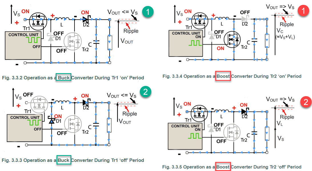

We can switch between acting as a buck converter for D < 0.5, and a boost converter for D > 0.5.
Flyback Converter
- Flyback Converter Summary
- A buck-boost converter with the inductor split to form a step-up transformer between the switching and filter stages.
- Flyback converters are useful for creating high voltages
- Also noted that the two power stages are isolated by the transformer!

https://www.coilcraft.com/en-us/edu/series/a-guide-to-flyback-transformers/
Switched Capacitor Converter
- Switched Cap Summary (also called charge pumps).
- How ICs can leverage the efficiency of a switching power supply without the space (or materials) for an inductor.
- Here’s a great paper outlining a very simple method of designing switched cap converters
- Generally inexpensive and convenient with the right IC for PCB design as well. Typically used to create integer multiples or divisions (or inversion) of a given voltage.
- Also commonly used to get around the floating source voltage we discussed in driving high side N-FETs (look for “charge pump high” and “charge pump low” pins on your datasheet.
