Week 5: Electronics Design
This week's assignment was to modify the hello ftdi board to include one LED and one switch. The switch should go between an unused pin and ground. The LED is connected to Vcc on one end, and each LED (it's an RGB) is connected to an unused pin through a resistor. Then, when the board is programmed, these pins can be connected to ground when the switch is activated (or however I decide it should be done).
The right tool for the right job
I spent most of this week experimenting with EAGLE PCB software. A former colleague of mine used to talk a lot about using "the right tool for the right job" - meaning you should know how thing work to take full advantage of them, and to know when you should be using a different tool. And I know what I want to do (design a PCB), but I was not super sure how EAGLE helped me do that, or how to best use it. Rajesh helped me a lot this week, and showed me how to get EAGLE to understand what I wanted. So, this summary is less about designing electronics in general, and more about using EAGLE to do so.
The Schematic
The most important thing is: the schematic is for humans! Do not use it to plan routing! Use it to show other humans what the important connections are. Practically, the connections on the schematic are not layout as they are in real life (especially for the integrated circuit), so it's sometimes pointless to use it for routing. Also, the schematic can be easier to read when you connect elements to Vcc and Ground, not necessarily to other elements that are also connected to ground. This also allows EAGLE to see what should be connected to one another, and which connections satisfy the schematic specifications. This makes routing easier later.
Elements can be floating off to the side, as long as they are connected to the right signals.
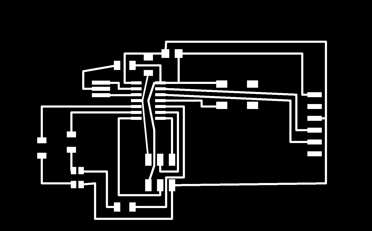
Routing and Board
I spent the most time on this step. Or rather, steps. Because I did it several times. The first time, I was excited to use the 'autoroute' function and thought I'd let EAGLE do all the work. However, I knew that I would be using some 0 Ohm resistors to get over traces. But I wasn't sure how to communicate this to EAGLE. I also wasn't sure until after some routing which traces would need those jumper resistors. For the LED, each has a resistor so that made some routing easier. I did end up putting one 0 Ohm resistor between the resonator and ground. So here's the process I would recommend:
- Make a clear and clean schematic
- Make sure you are using the correct components!! This will affect what EAGLE allows you to do for routing, so it's important that these are correct
- On paper or a dy erase board, plan out your components. It's best to put these components in the right places. If you're pretty sure you'll need a jump, put 0 Ohm resistors on those paths. You can always remove them later.
- Go ahead and try auto-route! You can always undo it
- Setings: 0.016" trace width
- If there are only a couple of unresolved routes (will show up in yellow), then put jumper resistors between them and whatever they need to connect to. Place these over traces on the board, and route them yourself (the resistor goes over the trace you want to bypass)
I found EAGLE very helpful when I set it up correctly - it knew what the layout of components were, so I could be sure that my routing would work out with actual components. I also found the yellow routing handy, as it would highlight what two things needed to be connected. And in the cases of things like ground or Vcc, it would show the other traces to be connected to. But it needed to be set up by placing components in the correct spots. If there is a way to allow EAGLE to move things around as it sees fit, I couldn't find it. I would have appreciated this the most. I ended up doing all my own routing, but this is also because I did it on a plane when my computer battery ran out. Then I just followed what I'd made on paper on EAGLE.
I wanted to fit more traces fown the middle of the IC, and played around with thinner traces, but I found the real problem was how far apart EAGLE made the traces be. I thought this had to do with the 'drill' setting, i.e. that the traces must be at least one drill width apart. But changing this setting did not let me put traces closer together. I still don't know how to get them close together, but should learn how to for future boards. Then I'd be able to make the boards smaller. This page will be updated when I find how to do that.
Cutting traces on the Modela
To get the traces, click on the 'layers' button (has three squares of different colors) and then click 'None' so nothing is displayed, then click 'top' (should be dark red) so only those are displayed (assuming your traces are on your top layer). Then, do File --> Export --> Image and use the settings as given below (but choose your own name, of course), especially the monochrome setting! and 500 dpi.
Layers for showing what you want
Settings for PNG export
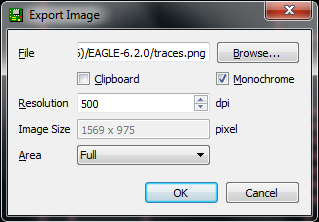
Some classmates found that the image had to be inverted, but I found that EAGLE gave me a black background and white traces, which is what's needed. As a reminder...
No, not this
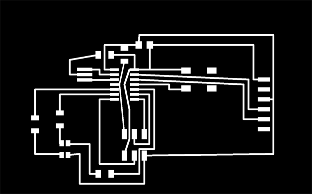
Much better
Using the Modela is as in week 3, and as a reminder: make sure the drill bit is pushed down into the material (lightly, don't break it) before milling or it won't go far down enough. If this is done, then the mill settings should be sufficient.
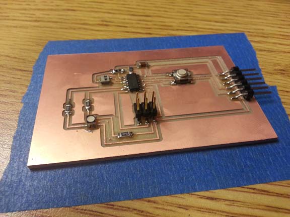
Post-Processing and stuffing the board
I had some trouble with the board, because I'd drawn traces very close to pads that they should be connected to, so I took the soldering iron and Xacto knife to one part, to make sure traces were separated.
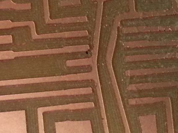
Traces too close