Ben Z. Yuan - How to Make Almost Anything
Week 5: Electronics Design
This week
Electronics design!
Individual assignment: PCB redesign
We were asked to redesign an example PCB, containing an ATtiny44, FTDI header, and ISP header, to add a button and LED.
To do this I used KiCAD (which I had taught myself a couple weeks ago, in the project log). It’s stopped being crashy, which is super important.
Here’s my schematic for the week. Some of the wires could be visually routed a little more cleanly.
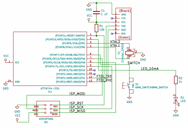
But wait, how does the switch work? The ATtiny44 has configurable internal pull-up resistors, so we don’t need to add one to the circuit ourselves. When the switch is open, pin PA7 will be pulled up, and when the switch is closed, the short to ground coupled with the pull-up resistor will pull the pin down. So PA7 will give us the logical inverse of the switch state.
We put a 1K resistor on the LED to limit the current to 5 mA, which should be within tolerance for our part.
After we have a schematic we need to turn it into a PCB design:
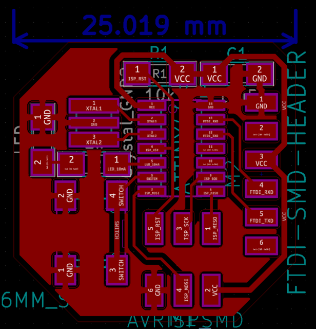
I used trace widths of 0.25 mm (9.84 mils) for most data lines, with a trace width of 0.5 mm (19.69 mils) for VCC, and a zone fill for GND, enforcing by DRC a minimum clearance of 0.396875 mm (1/64 inch).
When reviewing my board specter suggested that a zone-fill for GND might not be the best idea, as it can be difficult to ensure that shorts to ground are absent. I will concede the point – using a zone fill with narrow clearances does require an extremely steady hand in placement and little margin of error when doing the board stuffing. Nevertheless, I’m in a camp that doesn’t want to route more things than it needs to – and since the entire board wants a common ground, a zone fill is the easiest way to accomplish this.
A zone-fill ground also has the convenient property that, if you’re doing oscilloscope work, you can clamp the board almost anywhere with the scope probe’s ground clip and then have ground. (This would not be true if we used solder mask like a normal person.)
I exported my board traces and outline as SVG and performed some minor manipulations in Inkscape and GIMP (e.g. adding a white background) to allow successful import into FabMods.
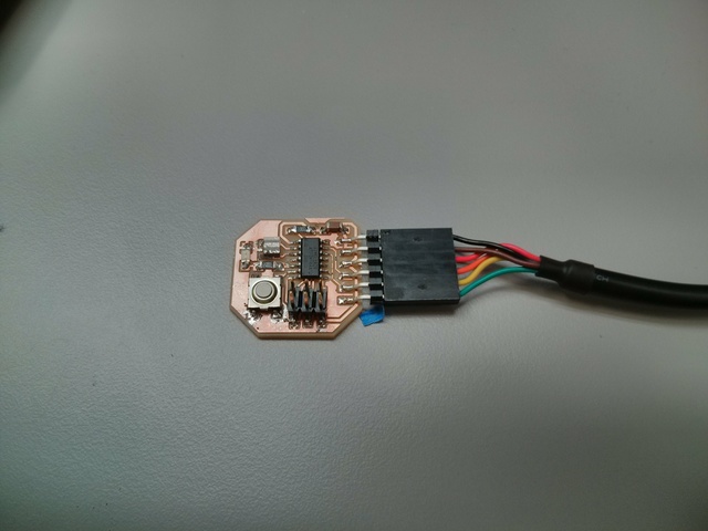
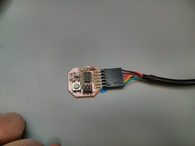
Following this, I machined my board on the SRM20 and populated it by hand:
The trickiest part was populating the crystal. It’s pretty helpful that its contacts encircle the entire package, but it can be especially hard to solder the middle (GND) contact. I ended up soldering along the side of the crystal; using the manufacturer recommended pad layout this ended up being relatively possible and seemed to produce a usable board.
It is also not necessarily obvious which way the button is oriented. Testing with a multimeter can confirm the orientation of an unknown switch. In this case, for our 6mm switch, the contacts across the line defined by the narrow edge strips (through the button) are normally open, and shorted when the button is pressed, while the contacts on the same side of said line are always shorted together and thus belong on the same net.
I modified the provided example source code to support lighting up the LED when the button is pressed (modified source code here). Note the following:
- The ATtiny44 has two ports, PA and PB. Pins can be independently set to be input or output pins, and to be interrupt-throwers, but interrupt vectors are per-port.
- To set a pin as input set the corresponding bit of its
DDRregister (DDRA,DDRB) to 0; to set it as output set said bit to 1. - Setting an input pin’s bit in
PORTA/PORTBto 1 enables the pin’s internal pull-up resistor. Setting an output pin’s bit to a logic value (1 or 0) drives that pin high or low respectively. - The pin’s current value may be read from
PINA/PINB.
So now, in addition to echoing back any characters it receives via FTDI interface, the board lights up an LED when the button is pressed:
Bonus content
Partway during this process, my phone battery decided to go all end-of-life on me by inflating like a pillow. Oops!
This presented a problem since I rely on my phone to carry two-factor TOTP secrets, and I kind of needed to export them since I didn’t have a recent backup (for unrelated reasons).
The Google Nexus 4 has the unfortunate property that it requires battery power to turn on, even if the micro-USB connection can provide enough current to run the entire phone. So we needed to make the phone think there was a battery present, even if one wasn’t.
I disassembled my phone and carefully removed the (glued-in!!!) inflated LiPo battery. The battery connector is of a form factor that DigiKey doesn’t carry (I looked!), so I had to scavenge the existing connector. I did this by cutting the battery cable with wire cutters, then carefully soldering wire to exposed metal contacts where the connector is attached to the cable:
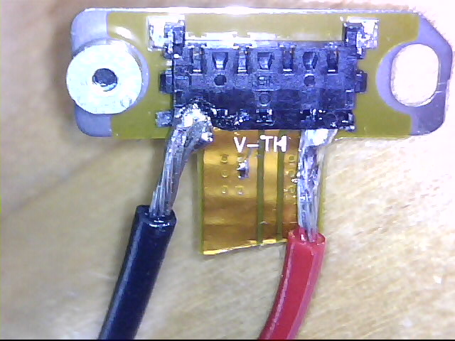
(I didn’t worry about the T pin. On a normal battery, this connects to ground across a thermistor, but I don’t have any thermistors on hand and didn’t want to play any unnecessary guessing games.)
This was good enough to connect the phone to a benchtop power supply set to 3.7 V, which convinced the phone that there was a battery connected with something like 40% charge.
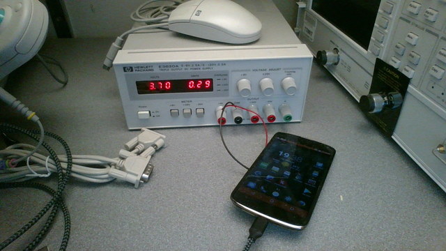
This setup strains the definition of “mobile” in “mobile phone” and is possibly
the worst idea ever, but worked well enough for me to exfiltrate the data I
needed using adb.