Ben Z. Yuan - How to Make Almost Anything
Project Log: A Hardware Password Manager
Here’s a running log of project-related content.
Week 1: ideas
Project
For my final project I’m looking to build a hardware password manager.
Why
Existing software password managers, like LastPass, 1Password, KeePass, …, are very good at managing all of our network service passwords, so we can have different passwords for Facebook, Twitter, LinkedIn, Google, Steam, and other such websites. However, they suffer from one common problem: you have to be logged in to some computer to access them. This means that you can’t (effectively) use them to manage your terminal login passwords, since you aren’t logged in when you need to type them!
At MIT, you use your Athena credentials to log in to many internal websites, but you also use your Athena password to log yourself in to any one of the various physical terminals on campus. If you don’t have a computer of your own, it becomes harder to use a strong unique password for your Athena account like you’re supposed to, because you can’t rely on KeePass etc. to remember it for you.
You could create some application on a smartphone to keep your passwords. But then you run into some problems:
- You have to trust that your smartphone and its operating system aren’t surreptitiously sending your passwords somewhere else.
- You still have to transcribe and type your password in by hand - meaning that someone looking over your shoulder can learn it!
- You now have to secure your phone against people who want to “borrow” it.
We solve these issues by creating a dedicated hardware device that anyone with access to fabrication tools should be able to assemble.
Design specifications
Required features
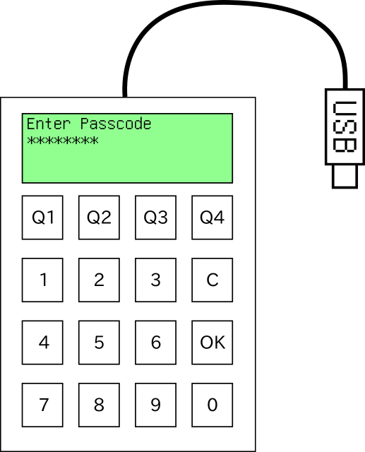
- Emulate a USB keyboard.
- Encrypt credentials on-device; require PIN unlock.
- User interface on-device; all features available without separate software.
- Generate credentials on-device with hardware RNG.
- Store and manage at least one password (preferably many).
- Durable enough for everyday use (no exposed circuit boards, resistant to dropping, etc).
Optional (wishlist) features
- Provide serial interface for backing up and restoring credentials.
- Provide mass storage interface for storing sensitive files (key files, etc).
- Wipe self upon too many PIN attempts.
- Resistant to physical attack / modification.
Prior art
This is not the first hardware password manager by any means; you can buy or build devices right now that mostly do the same thing.
Mooltipass ($80)
Things we like
- Emulates a USB keyboard
- Encrypts credentials on-device (with separate smart card)
- Open hardware and firmware
- Tiny!
- Extremely tamper-evident
Things we don’t like
- Requires separate software to preload or generate credentials
Pastilda ($50)
Things we like
- Emulates a USB keyboard
- Open hardware and firmware
- Encrypts credentials on-device in KeePass-compatible format
- Tiny!
Things we don’t like
- Requires preloading of device credentials
FinalKey ($??)
Things we like
- Emulates a USB keyboard
- Open hardware and firmware
- Encrypts credentials on-device
- Generates credentials on-device
Things we don’t like
- Requires separate companion software to operate
Week 3: random numbers and UI
The common thread between existing known hardware password managers is that they don’t really work without a computer to manage them: typically pre-existing credentials are preloaded, or passwords are generated and stored with the assistance of a software tool. Given the limited user interface provided by such solutions, this approach makes sense – but this is How to Make Almost Anything, and since we aren’t constrained by such challenging size requirements as “has to fit in the size of a USB flash drive”, we can do whatever we like.
So in order to be able to generate passwords on-device, we need a couple of things:
- A competent hardware random number generator.
- A user interface powerful enough to manage many passwords.
Hardware RNG
Probably the canonical way to get “true” random noise is to grab the least significant bit of something hard to predict. Depending on what you have access to, this could be one of:
- Some on-chip timer.
- Some noisy environmental sensor.
- Some noisy circuit (most famously, a reverse-biased diode junction).
- The output from some dedicated crypto-processor that does one or more of these things.
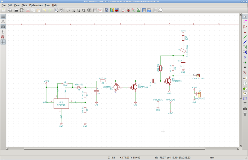
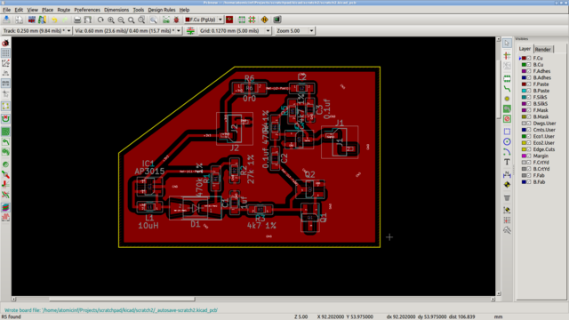
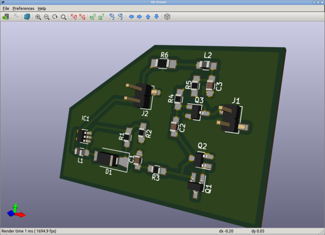
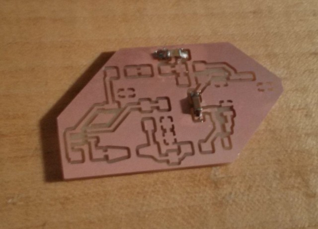
People have done this sort of thing before, of course, and based on some discussion doing this well is apparently deep analog. Since I’m not trained in analog I decided to “directly” borrow the OneRNG’s avalanche noise circuit for now (not replicating their layout directly yet, unless it turns out during testing that I really rather should). In a premonition of Week 5 I used KiCAD to create a schematic and traces for a test board (images below), but time constraints prevented me from milling the board this week. Also, I used 0804 templates by accident instead of 1206, so assembly could be inadvertently more difficult than I wanted! (If this ends up being a problem I can always redo the schematic.)
As an alternative the infnoise claims to be more robust, but I didn’t have time to try to replicate and planarise their schematic. Maybe if the OneRNG method doesn’t work out, I might look at their board again.
UI considerations
For frequent PIN entry there is really no better user interface element than a keyboard or keypad. Given that someone might enter e.g. an Athena terminal login multiple times a day (while moving around campus, or logging in to various network services), PIN entry should be as effortless as possible. This would seem to preclude solutions like the Mooltipass’s scroll wheel with button, but unfortunately places certain minimum restrictions on form factor size.
Grayhill makes a decent-looking 16-key matrix keypad. The unit price is $19.92 which is a little unfortunate, and the keypad itself is 2.5” x 2.7” which, combined with a display device, would make the whole thing a bit bulky. But I won’t know for sure until I prototype. This will require 8 digital GPIO pins to read directly, or as few as 6 if I do some multiplexing in hardware.
In terms of display I’m really tempted by the various 128xFOO pixel OLED breakouts sold by Adafruit. But these are expensive – a 2.5” wide 128x32 display costs $40 as sold. I might have to settle for an ordinary HD44780 ($10 as sold), which is the 16x2 character display you see everywhere.
I briefly entertained doing the whole thing as a TFT touchscreen instead, but I’ve got skepticisms about the durability – it would seem easier to protect a smallish display rather than a larger one, in the absence of whatever type of glass smartphones use, keeping in mind that this device has to fit in a pocket.
Displays with serial support (e.g. SPI) need a minimum of like 5 or 6 digital pins depending on the display type.
Next steps
I think attempt to mill the RNG test board (and stuff if milling succeeds), and also get a keypad module, display module, and pre-assembled microcontroller to play with (and put together a loose-wire prototype of final product).
Will need to think about case related matters as well. Should be able to CAD up an appropriate enclosure with OpenSCAD once I finalize the UI hardware.
Week 4: towards random numbers
I decided after designing the last test board that 1206 is a much better size for surface-mount parts, and since the fab lab inventory stocks 1206 everywhere I might as well redesign the board for that size.
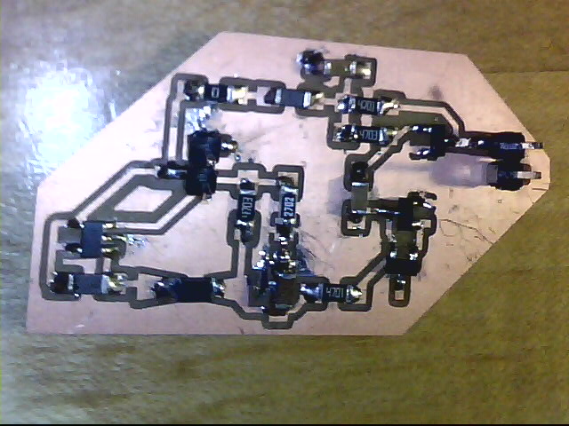
Shop time is possibly the most difficult commodity to get, and I had real problems getting into the shop this week because of constraints. But eventually I was able to find enough time to mill the test board and start populating the parts in stock.
We have some of the parts I need in the fab lab inventory but I’m still going to have to order a few (in particular the MMBT3904s, the AP3015, the inductors, and the odd-sized resistors).
Week 5: noise!
gavindar was kind enough to order enough of all the missing parts that I can make a few of these circuits if they work out well.
I finished populating the board on Tuesday afternoon:
I attached the 3V3 and GND pins on the “left” header (closer to the AP3015) to a benchtop power supply set to produce 3.3 volts. Sure enough, an oscilloscope connected to the SIGNAL pin on the “right” header produces a lot of noise:

This circuit effectively converts a constant 3V3 input into noise between ground voltage and about +2ish volts. This should be well within the range of the AVR on-board ADC. The circuit draws much less than 30 mA of current while operating, putting it well with range of something like a MCP1825 voltage regulator.
Sampling at 1 MHz (above picture) the noise certainly feels noise-like. Sampling at 250 MHz reveals some interesting shape properties:

Notice how the voltage rises seem to level off near the peaks, and generally feel much shallower than the voltage drops.
This is a plausible noise source, but will need debiasing to be useful.
Hallucinated microcontroller requirements
If I want to do all of this on one microcontroller then it probably wants to end up being rather large.
I need the following pins:
- 8 digital pins (4 output, 4 input) for a keypad
- somewhere less than 8 digital pins for a display
- an ADC pin for an entropy source
I also want a USB controller.
It’s hard to say a priori how much Flash memory I’ll need. The AES library from avr-crypto-lib takes up on the order of 2.7KB of Flash and 240 bytes SRAM. LUFA apparently takes up like 8KB of Flash on its own.
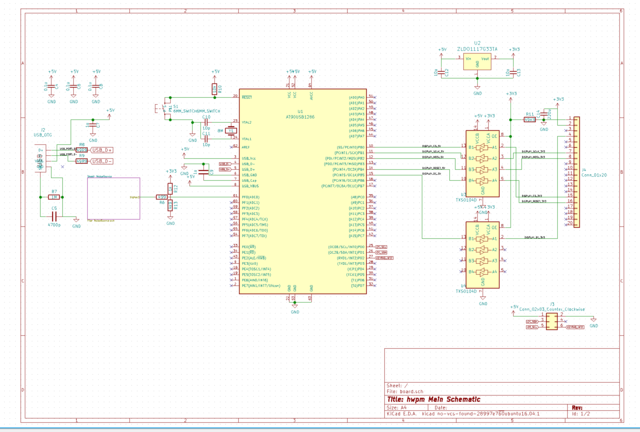
It might be sensible to start with the largest microcontroller we’re comfortable working with, getting our thing to work there, and then think about scaling down. In other words, we’ll want to “science” a board using an AT90USB1286.
Hand-soldering a TQFP64 could be a challenge. But the milling process shouldn’t have a problem producing the necessary traces: the pin spacing is well within our design rules.
I think I can borrow the Teensy++ 2.0 schematic as a base schematic from which to work. (In the event I run out of time or get too frustrated, I could also buy such a board outright, and wire some things together, for a fragile prototype.)
We’re going to have a lot to learn in the next few weeks, that’s for sure!
An alternative is to use two smaller microcontrollers – one with an on-board USB controller for handling the keyboard functions, and one handling everything else – connecting the two with a sensible serial protocol. This would increase the software complexity somewhat, as now I would have to write two separate firmware files.
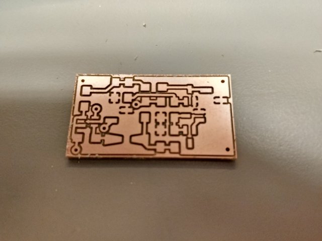
Week 7: 2-sided PCBs and final board.
I milled a double-sided PCB – specifically a 2-sided version of my noise board that eliminates a 0-ohm resistor.
I also created a potential final board design.
Separately, I experimented with a candidate display, a candidate keypad, and using the noise board as a hardware RNG source.
The Othermill
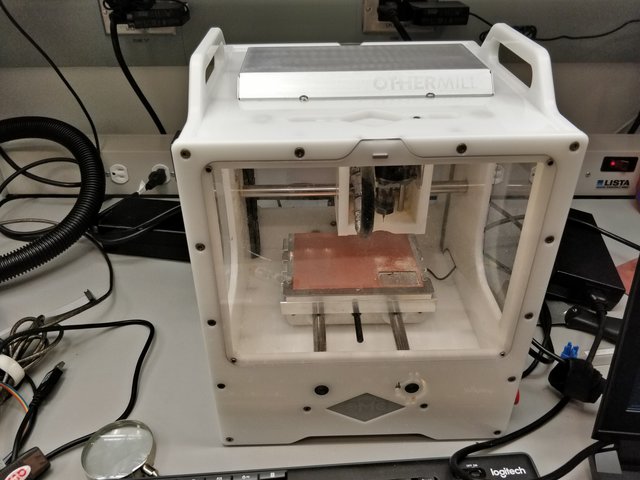
- Takes Gerber files and .drl files. Supposedly takes SVG but KiCad doesn’t export them the right way.
- Mill traces with 1/64.
- Mill holes with 1/32.
- Mill outline with 1/16 NOT 1/32 - the OtherMill software is much more aggressive than the SRM20 software and will happily break 1/32 endmills!
- Via diameter 1.75 mm, drill size 1 mm. (They were originally 1.25 / 1 but the via copper delaminated.)
A double-sided board
My first attempt caused via delamination:
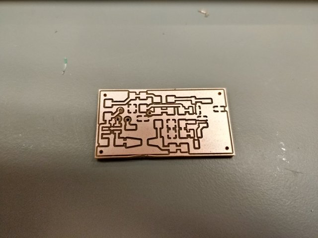
My second attempt turned out a lot better.
On entropy and related matters
Rhys Weatherley provides some useful crypto libraries, including a working entropy pool.
First I tried to update the pool on every ADC interrupt (manually scheduling the next conversion inside the interrupt routine), but the ADC is way too fast (tens of cycles) and I ended up mostly locking up the processor.
So, instead, I update the pool on a timer. It’s a fine balance trying to choose a timeout value that keeps the main system responsive while filling up the entropy pool in a timely fashion. This wouldn’t be a bad task for a coprocessor.
rweather’s RNG, by default, sources entropy from timer jitter. This
semi-reliably provides 48 bits of entropy every few seconds. It can also take
avalanche noise of the type my noise board produces. I modified rweather’s
TransistorNoiseSource to work directly with the AD0 pin instead of going
through an analogRead(), since the ADC is needed for nothing else. This
source takes a significant amount of time (sometimes over a minute) to
calibrate from a cold start, but once it’s calibrated it can provide
high-quality entropy in varying block sizes at impressive rate (even much more
quickly than the timer source).
Since rweather’s RNG uses a 384-bit internal state (using ChaCha20 as a mixing function), it can provide a maximum of 384 bits of true entropy in a single operation. While the RNG can provide pseudo-random bits even after entropy pool “depletion”, doing so increases the impact of RNG state compromise.
Final board design
I created a candidate final board design.
This initially proved unroutable. After determining how to reliably make double-sided PCBs, I was finally able to route the board:
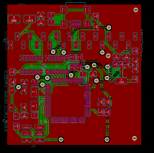
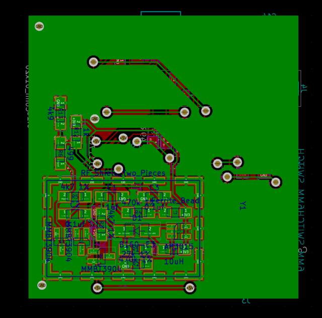
This will be extremely unforgiving to build:
- Clearances and trace widths basically at the allowable limits of our milling process.
- So many vias. Just because they’re possible doesn’t mean they’re easy to assemble; each one needs a wire pole and those have been harder than expected to solder.
- Components on the back (namely, the noise board and its RF shield).
- Main chip is a giant TQFP64. The TQFP32 chip in the AT90USB series has no ADC and is therefore useless to us in a single-MCU design, but might be usable in a later revision with multiple MCUs. While investigating keypad and display functionality, I determined that having additional coprocessors could be a useful innovation, as the AVR platform has limited support for true nonblocking I/O.
Another possible innovation is to change architectures (e.g. to something ARM-based). But doing this particular project in as small a MCU as practical is appealing: it’s much harder to hide something nefarious in a less powerful MCU, making lower-capability design more appealing from a verifiability perspective.
Week 10: board completion and revisions.
I completed revision 0 of my desired project board.
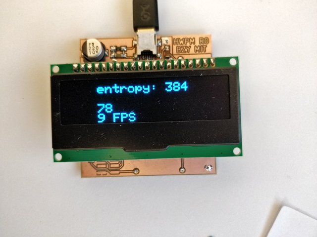
It communicates just fine with an Adafruit Trellis and a SPI OLED module.
Programs are loaded using the LUFA CDC bootloader which I had to burn onto the usb1286 using a temporary board with ISP header. (Fun fact: the usb1286 ships with fuses set for a 8M crystal, and with protection bits enabled – so to change fuses one has to erase the stock bootloader.)
The trouble here is that the pads for the I2C connector are positioned such that a 6-pin header will physically interfere with the display module. This, in addition to some inadvertent physical damage, will lead me to redesign and rebuild this board.
Week 12: a revised board.
I completed revision 1 of my desired project board.
This board moves the I2C header away from the display location. It also adds breakout pads for port A and port C on the usb1286.
It still remains to complete the main system software, design an enclosure with fixturing for all the hardware components, and find some way to replace the Trellis with some self-made input device.
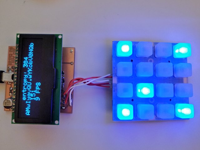
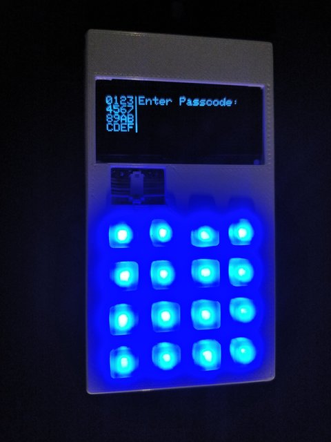
Final push part 1: a tale of terror.
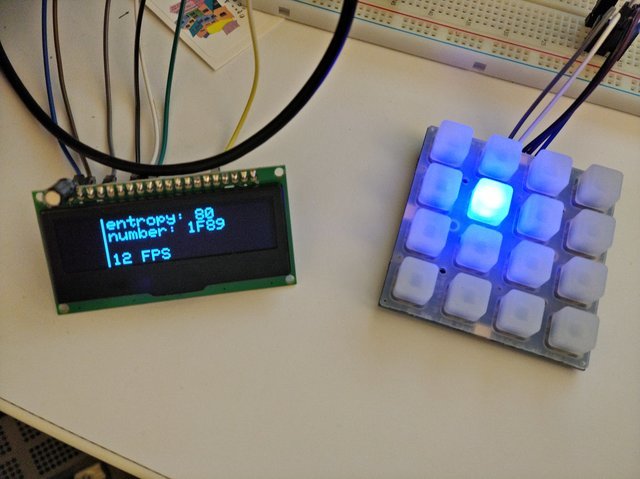
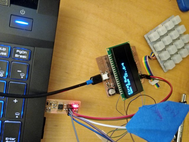
Revision 1 of the board is working great and I’ve completed a first iteration of the software using the Adafruit Trellis that:
- upon first run, asks you to enter and confirm an 8-digit passcode, which it uses in accordance with a randomly generated salt (saved to EEPROM) to generate a system key
- at first run, generates exactly one password entry (entry 0)
- upon subsequent runs, asks you to enter the passcode, tries to decrypt password entry 0, and then lets you type it (with a button press) on success
All this in just under 32K of code (including cryptography and peripheral libraries).
The trouble is that the LUFA CDC bootloader apparently causes terrible things when you try to upload over 32K of code – to the point where the board can fail to initialize correctly.
Without a traditional debug header I am forced to solder tiny wires to the ISP pins and route them to my FabISP.
The programming also takes on the order of 2 minutes rather than 2 seconds – but the board runs without a hitch afterwards.
Unfortunately the process of discovering this led to the waste of a good usb1286, which I don’t feel great about – but the removed MCU can live in my parts collection until I need another.
The process of discovering this has also led to a state where I don’t think I have time to incorporate the other input device! There’s nothing to be done about it though - looks like the alien Trellis and its LEDs are here to stay.
Final push part 2: a tale of encapsulation
I feel like I’m forgetting all of the lessons from Week 2, which isn’t great, but “everyone runs out of time”.
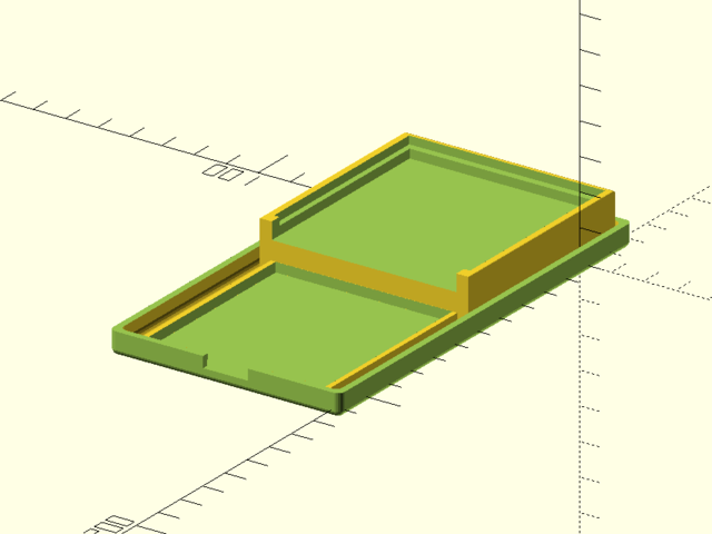
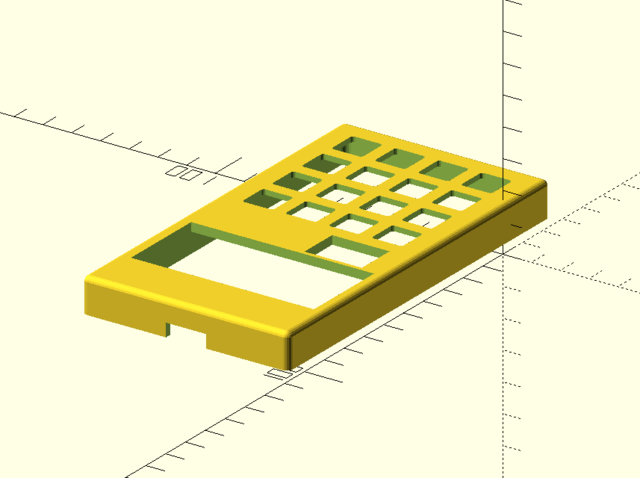
The circuit boards are kept in alignment by trays incorporated into the enclosure design (and, in the case of the Trellis, the enclosure holes coupled with alignment marks in the elastomer layer).
Having 24/7 access to a 3D printer is useful since I’m less tied to shop machine availability (especially since two of the three machines are broken). However, 3D printing is a slow iteration process and I was unable to completely iron out some of my alignment issues.
There are few things more infuriating than misaligning something by less than a millimeter and having to wait an hour for a correction!
The larger problem with the enclosure design is that it is not self-aligning – so you get awkward alignment problems when clamping to glue the case together. (I used a polyurethane-based glue for the final securement.)
A couple of other unfortunate things popped up in the process:
- Adequately aligning the display hole proved difficult. In the end it is presently held in place by mechanical stress on essentially one edge. With more available iteration cycles, the alignment could be tightened; but there is an underlying problem of a 20-pin header being very slightly rotated on the main board that would call for a refabrication of the board.
- A cutout had to be included for the I2C connector, as it is tall relative to the board surface! A solution could have been to use an angled header rather than a vertical one, but angled headers are not on inventory.
- Somehow the separation between the top and bottom halves of the enclosure was too large by about 4 mm, so I had to print an additional spacer to bridge the gap. I think I left insufficient depth for the Trellis; the spacer was the most expedient option, the alternative being to reprint the (time-expensive) bottom enclosure piece.
I also added a couple of extra features before removing the programming wires:
- Generate passwords with a long-press on the second row (row 1) while unlocked.
- Reset the board with a long-press on the lower-right button.
The latter is useful for demoing the system, as the alternative is chip erase requiring programming wires or a working bootloader.
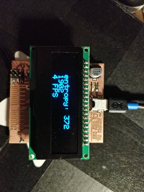
It types passwords:
It also looks “shiny”:
At this point it’s as good as it’s going to get for now.