Idea
Over the past three milestones, I have created a proof of concept for a simple 3x3 pixel image sensor using phototransistors. Feel free
to check it out here to understand the fundamentals and limitations of this type of sensor. Obviously, the 9 pixel sensor I have created before is not
impressive yet – it merely acts as a prototype. To make the magic of imaging happen and actually see someting useful, we need to scale things up. I initially wanted to go for a
32x32 pixel camera (= 1032 pixels). However, as I have to mill the board (as opposed to etching), I could only realize a 16x16 array (= 256 pixels) on a
10x10 cm area, which is sort of the maximum I wanted to go with for my camera body dimensions. Making this double-sided board from scratch
should be enough of a challenge in itself and I am fine with that (side-note: as I have already bought all the components for a 32x32 image sensor, I will
make one in the future – stay tuned).
This is the fourth milestone in a series of posts that cover my final project, where I will be creating a 16x16 pixel DSLR camera from scratch. In my case,
from scratch literally means milling the PCB for the electronics and stuffing it by hand, figuring out the optics and then putting everything into a nice
housing of 3d printed parts and flat panels. By the end, we will hopefully have a working model of a DSLR camera that can (natively!) produce cool pixel-art images
and demonstrates the inner workings of a modern-day DSLR camera.
Creating the Base Schematic of One Pixel (Template)
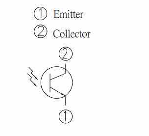
I am using a phototransistors, which is a semiconductor component that combines a
photodiode and a transistor and has a collector and an emitter. As always in a NPN transistor, current flows from the collector to the emitter, but instead of controlling the base electrically, this one opens
if photons hit its photosensitive area. If we send some current through the collector of the phototransistor and then measure the voltage over a resistor connecting the emitter to ground (voltage divider), we
observe that the voltage is proportional to the number of photons hitting the phototransistor. In other words, the measured voltage is low when the phototransistor is dark and high when it is lit up. The resistor value
dictates the voltage range (and, thereby, the sensitivity) of our diodes. Choosing a small resistance (say, 1 kO) makes the phototransistor less sensitive to light, whereas a large
resistance (say, 1 MO) makes it more sensitive or pick up dimmer light. If
you want to learn more about how phototransistors work, this video by Scott Harden is a great demonstration. In my case, I decided to use
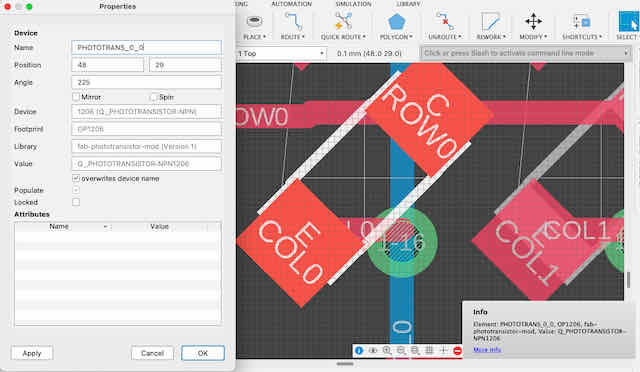
the 1206 package phototransistor PT15-21C/TR8 by Everlight Electronics Co Ltd for its
great photo-sensitivity and because we had it stocked in our fab inventory. The respective datasheet of the phototransistor can be
downloaded here. A footprint with pads for the component can either easily be created
from the dimensions in the datasheet, or downloaded from the FAB library referenced in Week 3.
The phototransistor circuit diagram

The dimensions of the phototransistor
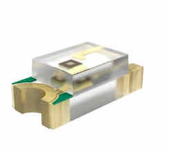
A rendering of the phototransistor I will be using
In theory, the design for our image sensor is relatively easy: Create the schematic for one pixel, and then copy-paste it 256 times to create an array of
16x16 pixels. Therefore, in this first step, we will create a clean schematic for the first pixel. First, I opened Fusion 360, which I use to create my boards. I started by creating a new electronics design project and initializing a new empty schematic and associated PCB. Before starting our work, we always want to set up our libraries and design rules first. In my case,
I am using just the FAB and the supply1 libraries for now, which I activate in the library manager. Next, I set up the design rules and import the FAB design rules, which are also referenced in Week 3.
Importing these settings and tweaking them on the go is really important for this project, as I am trying to push the endmill to its limits by packing the array of pixels as tight as possible. We also want to turn on our grid and set a useful grid size (I used 0.5 mm in my case).
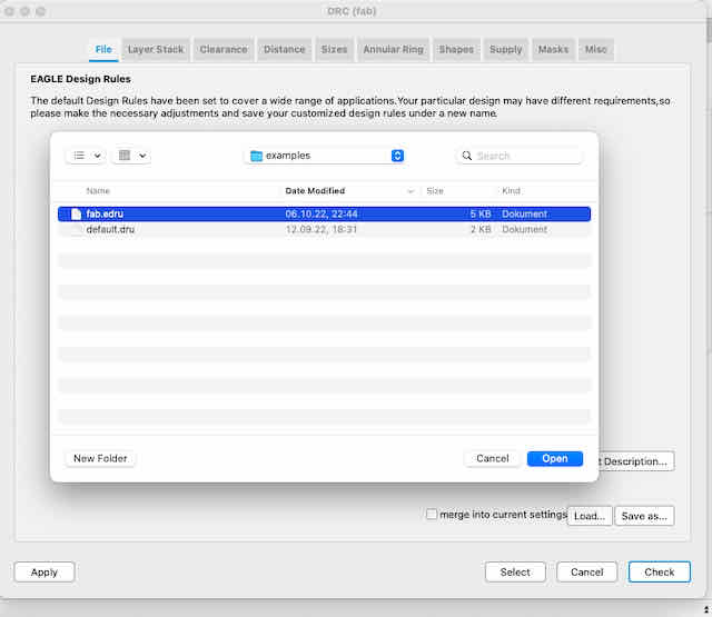
Setting the design rules before any work happens
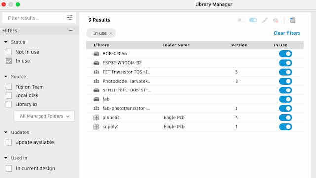
Loading the libraries I need
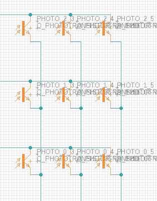
After setting everything up, I switched to the schematics tab again and added a single phototransistor from the FAB library to my schematics. We will later arrange our phototransistors into a grid / array, so we will have rows and columns connecting everything.
I chose to connect the collectors on common rows and the emitters on common columns. Hence, I started with ROW0 and COL0 for the first row and column, respectively. And that's our first pixel.

A first pixel
The same idea scaled up to a 3x3 matrix
Testing our 1 Pixel Circuit
Now, just before we continue building this same circuit for all our 256 pixels, wouldn't it be a good idea to test this
circuit? Indeed, we absolutely want to test it, and it's relatively easy. All we need are the following components:
- 1x phototransistor (I used a surface-mount one, which is finniky but works)
- 1x 4.7 kO resistor
- 1x 1.5V battery
- 1x small breadboard
- 1x multimeter in voltage measure mode (I used up to 2V)
- Jumper wires
I simply wired them up according to the one pixel schematic presented earlier and then measured the voltage difference across the
resistor. Notice that the orientation of the phototransistor matters – refer back to the datasheet and you will
see that the collector (with the green mark) has to be connected to the positive side, and emitter goes through our voltage-dividing resistor to ground.

A simple representation of our one pixel circuit
As you can see, the voltage reading is high when light hits the phototransistor, and low when I cover it with my hand. Ignore the sign for now, this is just because I connected the two measuring electrodes of the multimeter in the opposite orientation.
Now that we tested that this logic actually works, we can move on to scaling our schematics up.
Copy-Pasting the Schematic 256 Times (Not Recommended)
Next, we need to create our field of phototransistors. To achieve this in our schematics, I first copied my pixel and pasted it a few times, then copied the copied pixels to paste them again, scaling up
exponentially. Eventually, I had the 256 pixels I needed in a 16x16 grid. This was relatively fast, it maybe took 3 mins. Unfortunately, I had to re-name the rows and columns of each pixel, which obviously took
some time. The net breakout function allows you to rename nets with a template name with a single click, so this sped up operations. Nonetheless, my grid became quite hard to work with at this point, and needed more
fixing later. Although I now technically had 256 components wired up as I needed them in my schematics, I realized that the way my components were named from the simple copy-paste operations was not
very helpful and would make it hard to place the components on the PCB layer. After all, I did not want to sort 256 components independently to figure out where each one goes.

Using the net breakout pins function to quickly change column / pin names
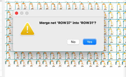
One drawback of copy pasting is that Fusion creates new row/column labels and asks for merge permission for each pixel
Another issue is that the naming is inconsistent and so you when you automatically arrange your components, they aren't sorted
At this point, I realized that my whole approach of copy-pasting components was not the way to go and would just make things harder later. Therefore, I decided to ditch my approach, go back to the one pixel I had, and instead
try to figure out a way to automate the whole process intelligently.
Writing a ULP Script to Design the 16x16 Pixel Schematics (Recommended)
Eagle / Fusion 360 has a basic yet very powerful scripting language built in which can be used to automatically add components and arrange them, both
in the schematics and on the PCB board. These are called ULP scripts and can be found in the automation menu. This time, instead of manually dragging and aligning components, I decided to
write a ULP script to do the job. Although I did not know anything about the ULP scripting language, it was relatively easy to get into by understanding this related project of Ted Yapo, who made a 16x32 LED array
(find his respective GitHub repository here). The basic idea is that we write a number of Eagle commands that get executed
sequentially, like adding a component and adding the respective nets to its pins. A helpful documentation of all commands was made by MIT and can be found here.

You can try out all commands by typing them into the command line here
I used a nested for-loop to iterate over all rows and columns of my pixel sensor array. For each unique row and column position (i.e. for each pixel), I added a phototransistor at a certain offset and rotated it accordingly using the ADD command. I then
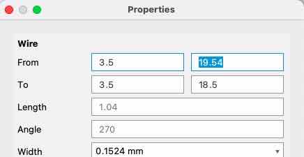
added a net for the row coming from the collector end of the transistor. While experimenting with my script, I observed that in order for the net to be connected to the component, its origin had to be EXACTLY where the pin of the transistor was. To get this absolutely
right, use the following trick: For your reference pixel that you have already created manually, right-click the row net and go into the properties to get the exact from/to coordinates. Also check the coordinates of your component. The difference between the origin of your component and the
start of your net will be the offset you need to place your net EXACTLY where the transistor pin is and it will automatically connect. Note that estimating this or simply using junctions DOES NOT WORK reliably. Measuring where Fusion 360 places the nets
when you place them manually, and then programming the offset to the component in is the tedious but rewarding way to go.
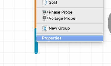
After placing down a net by hand, I go into this net's properties...
...to check for the exact start and finish points to use in my script...
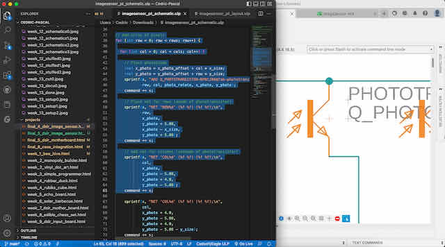
...which I wrote in Visual Studio Code...
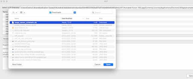
...and then imported from Fusion's automation tab
After some trial and error, I had a script that could generate a variable array of phototransistors hooked up with correctly labeled rows and columns.
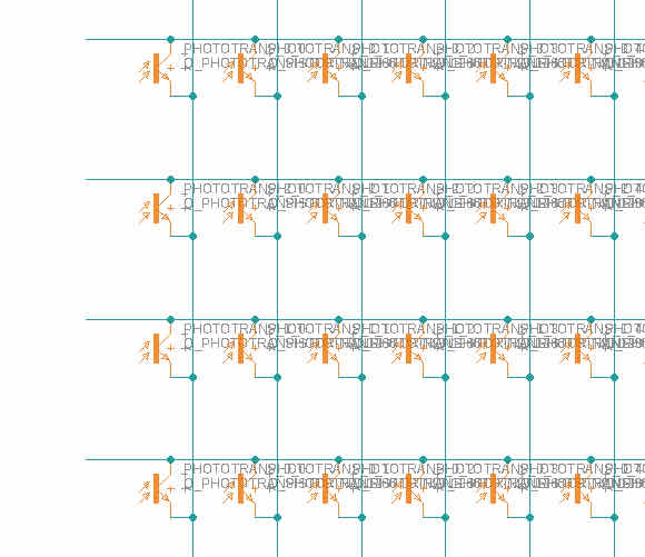
One small array generated by a ULP
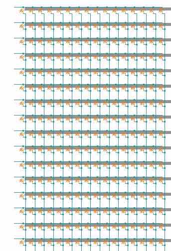
The final array generated by a ULP
I added a second loop at the end of the script just over the columns to add a resistor (voltage divider) between the emitter and ground for each column, as
discussed in the theory behind our circuit.

Adding one resistors to ground per column as a voltage divider
Finishing the Rest of the Image Sensor Schematics
Creating the schematics for the pixel array was arguably the hardest part. We now complete our schematics by adding the other components for our image sensor board.
Besides the phototransistors, our image sensor will use the following components to take an image and interact with the camera mother board it is connected to:
2x ARM SAM D11C 14C microcontrollers by Atmel (datasheet)
2x CD74HC4067 16x1 analog multiplexers by Texas Instruments Inc (datasheet)
2x SBH11-NBPC-D05-SM-BK 5x2 pins male headers by Sullins (datasheet) (footprint)
2x 10kO pull-up resistors for RST pins of D11Cs
2x 1uF bypass capacitors for D11Cs
2x diode for D11Cs
A few 0O resistors to bridge over traces where no space for vias
The two 16x1 multiplexers will be used independently; one will drive the rows, the other the columns. To make an analog reading of one of the pixels in the 16x16 array, one of the 16 rows is set to high at a time (while the other ones are low).
At the same time, we analog read the voltage at one of the 16 columns at a time (while the others are driven low). If you would like to understand the operation of a multiplexer in more detail, take a look at Sean Hudgins' great tutorial aout a 32x1 multiplexer.
In my case, I connected the 16 row nets to the 16 selector pins, and repeated the same for the 16 columns nets for the other multiplexer.
We could let our motherboard drive the individual rows and columns of the image sensor. However, I rather wanted the image sensor to be as independent from the mother board as possible. From an architecture perspective, I want the image sensor to autonomously capture images and simply relays the read values
back to the mother board via I2C. To achieve this level of separation, I decided to run the two multiplexers from two independent D11Cs, which each happen to have just enough pins to support one of the multiplexers. Looking at the schematics now, I would have rather chosen to use
one D21 instead of two D11s to reduce complexity, but it worked fine nonetheless. To connect the row multiplexer, I hooked up the data lines to one of the D11Cs, and repeated the same for the column multiplexer and the other D11C.

The wiring of the two 16x1 multiplexers
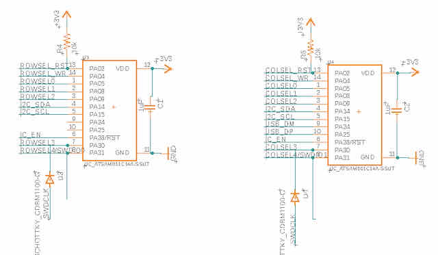
The wiring of the two D11Cs. Notice they share the same clock wire for programming, so I used diodes so they could not talk back to each other
Last, I connected the 5x2 headers accordingly, such that one of them can be used to transer data to the motherboard using I2C (both D11Cs) and USB (only the column D11C). The other one can be used to program the two
D11Cs independently (they share a common clock wire, but we prevent signals from flowing back into the other multiplexer using two diodes). We also add two pull-up resistors for the D11Cs reset pin, and two bypass capacitors just to make sure
there are no voltage spikes as the D11Cs are a bit farther away from the mother board power source.
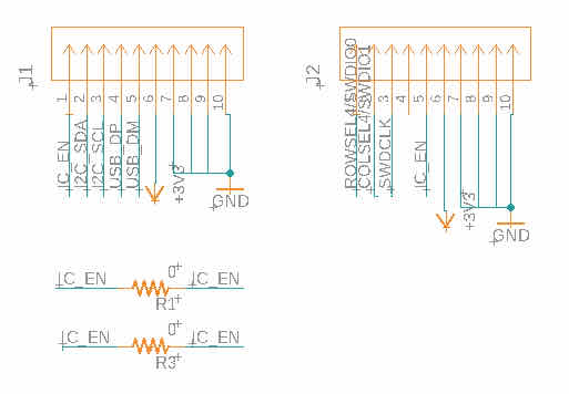
The wiring of the two 5x2 headers

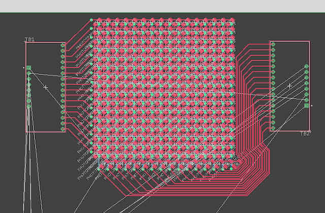
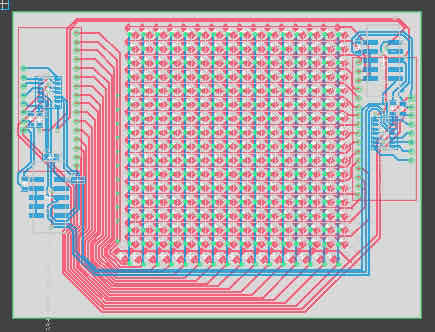
The finished schematics
Routing the Traces for One Pixel (Template)
After arranging my motherboard schematic, I switched to Eagle's PCB board tab and continued
by routing the traces of my PCB board. The core part of my image sensor is obviously the 16x16 array of phototransistors, so I wanted to
route this first and then arrange the other components, possibly making use of any spare space on the other side of the board. Similar to how
we first modeled a single pixel in our schematics, we will again route just the first pixel by hand to measure the exact dimensions of all traces necessary,
and then generate the pattern using an automated ULP script.
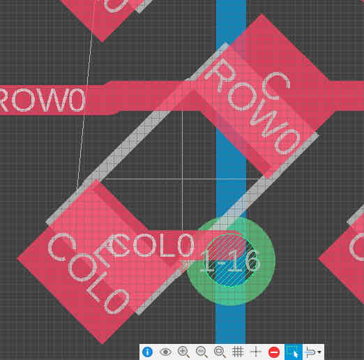
I rotated the phototransistor by 45°, which allows us to stack our pixels tighter and route them more efficiently. A row trace runs paralell to the x-axis and
connects to the collector of the transistor. A column trace is routed on the opposite side of the board, and connected to the emitter of the transistor via a via. Take a look
at the following image that displays the routing I went with. This routing allows for pixels occupying an area of 3.8 mm x 3.8 mm each (in other words, we can later create a new
pixel with an offset of 3.8mm in x and/or y-direction to the last pixel).
Again, we route a single pixel by hand
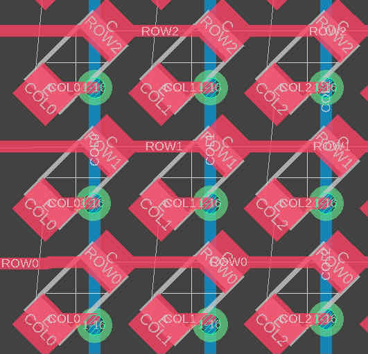
This is the pattern we get for a 3x3 grid by hand
Writing a Custom ULP Script to Route the 16x16 Image Sensor
In a similar fashion to the way we automated our schematics layout using a ULP, we can now use a ULP to move our components
into position and place traces and vias where we need them. Although it does take some time to figure out the exact spacing and dimensions, this
solution is much more scalable and easier to adjust than manual placement or dealing with the alignment functionality built into Fusion 360.
One handy advantage of writing a custom ULP script for the PCB board after having written one for the schematics is that we can easily reference
components by the same name we have assigned earlier.
Akin to my schematics ULP, I again use a nested for-loop to loop over all rows and columns to build every pixel. I simply move the phototransistor into position
and then extend the row trace and the column trace from it. I also place the vias with the correct drill size and conductive copper ring diameter as adjustable parameters. Again, to
get the right offset dimensions, I simply go to the traces I placed for my first pixel (reference) and view their from/to coordinate properties.
Again, we can use the properties tab to get the exact coordinates for our traces
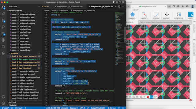
Writing the code is analogous to how we created the for our schematics
We again import our ULP in the automation tab, though this time from the PCB tab
After some tweaking, I arrived at a script that generated a perfect 16x16 phototransistor array. Next, I added some code to loop over all columns to add the respective column-resistor
and a ground line to each of them. I also added a via to each row start to make the row signal accessible from both sides of my image sensor. Our final script now generates the entire
phototransistor array of any size. We simply need to connect the rows and columns to the multiplexers now.

The revised and final arrangement of all my phototransistors
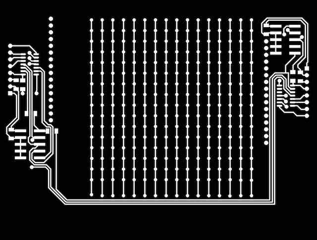
Routing the Remaining Traces to Finish the Image Sensor
This last step might seem more daunting than it actually is. First, I placed one of the two multiplexers on each side of the PCB and routed the row- and column-
lines to their respective selector pin on one of the multiplexers. Again, make sure you set your final design rules before you do this, as you will want to stack the traces running
in parallel as closely together as possible.
The revised and final arrangement of all my phototransistors

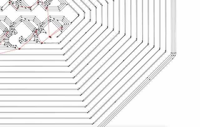
With optimized design rules, we can route our traces just perfectly apart from each other
A quick check in Mods to see that the toolpath can indeed be milled, which was the case
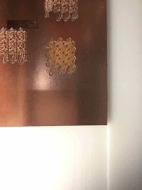
If you want to be extra sure, you can even mill test patterns to see how they come out
Next, I added the two D11Cs and the two 5x2 headers to the two sides of the multiplexers. I had to pack everything fairly tight on my board, which is reflected in some
greedy design choices which you can see in my board design. If you have more space, you can surely run the traces in a slightly cleaner way. Nevertheless, the routing works fine and fits
on the 127x100mm FR1 board I had been given.
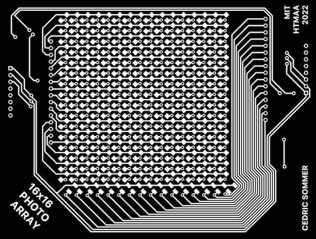
The final tracing and routing of the completed image sensor
Exporting the Traces for Milling
Last, we want to export our double-sided board design into a format we can use for milling. I previously covered this part for single-sided boards in Week 3 and for
double-sided boards in Week 11. Therefore, this will just be a quick run-down of the exports we need. I used the export image command and exported the following images
at 1000 DPI each, monochrome:
- Just export layers top, pads, vias (will later be used to mill top traces as seen from top, 1/64" endmill)
- Just export layers pads, vias (will later be used to mill vias as seen from top, 0.7mm endmill)
- ATTENTION: Flip the board over (mirror it) at this point
- Just export layers bottom, pads, vias (will later be used to mill bottom traces as seen from bottom, 1/64" endmill)
- Just export layers outline (will later be used to mill outline as seen from bottom, 1/32" endmill)
Afterwards, I cropped all files together in Photoshop and adjusted the fill colors to produce the following export imgaes that will be used as input by our mill.
Yay – we have successfully made the files to mill our board.
The edited top traces from Photoshop

The edited vias layer from Photoshop
The edited bottom traces from Photoshop

The edited outline from Photoshop
Summary
This wraps up this forth milestone. We started by looking into the phototransistor and other components to use. We then
created a custom ULP script to create a phototransistor array of any given size in Fusion 360. Afterwards, we created a second
script to move our components and put down an array of traces such that we have a 16x16 image sensor array. We added all other
components and then exported our traces and outlines to generate our toolpaths for our endmill. In the fifth milestone, we will
actually create our board and – hopefully – take our first images!