Week 10: Building an OLED Screen & Menu Interface for a DSLR Camera
Idea
This week, I will continue building the simple DSLR camera I started two weeks ago. So far, the camera
has a motherboard with a LiPo battery attached. It also has a simple 3x3 image sensor of phototransistors to record an image. By far, the most important
element still missing is some interface to control the parameters of the imaging, as well as a small screen to actually view the photos we took. As this
week is concerned around output devices, the OLED screen perfectly fits in, and I hope that we will be able to finally capture and look at some images by
the end of this week. This part is especially exciting, because I have never used an OLED screen (or any screen, for that matter), so I hope to get more confident
in reading the datasheet of any component and understand how I can use it in my board.
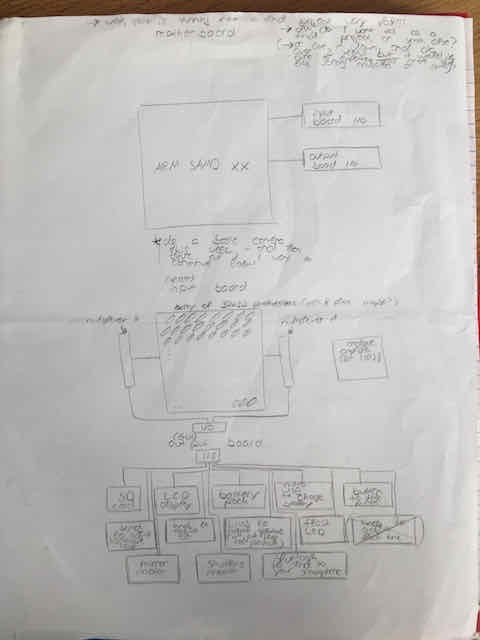
This week is the third part and final in a series of posts over the past weeks. I created a motherboard based on the ARM SAM D21E two weeks ago,
with a 2800 mAh LiPo battery. Last week, I created a simple 3x3 image sensor to actually capture an image. Finally, this week will complete
the project and allow us to interface the camera properly.
Planning the Architecture of the Output Board
Compared to last week, this week's board has a much simpler architecture. I started by listing the features that I wanted to have present on this board in
order to interface the camera. Although I probably had 1000+ wishes for things for my camera to have, I eventually settled on the following
features and their respective components. This is the most straightforward approach from my point of view, since adding those components to our
schematics will be the first step once we switch over to Eagle for the design of our PCB board. The features are listed below, the
respective components are listed in the next part.
Screen to view images & adjust settings
Buttons to avigate though a settings menu displayed on OLED screen
Button to take an image
Switch to switch between image capture and image review mode
LED to show status of current operation
Pin heads to connect to motherboard
I did not do much planning for the tracing, but figured that most should be rather easy to trace once I have my schematics
live. Therefore, I jumped straight into the schematics in Eagle.
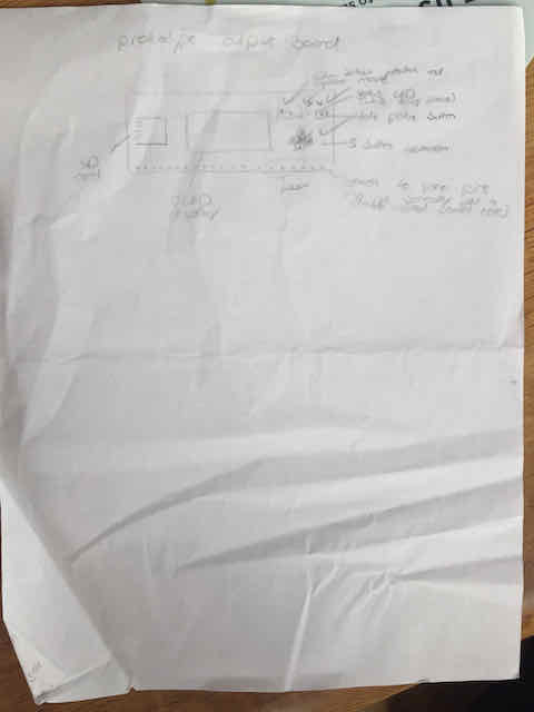
A quick sketch of my output board and the physical position of my components
The final integration of my output board for a potential final project
Designing the Schematics
Since this board should be able to connect to the breakout pins of my motherboar (the same ones that the input board gets), I
started by opening that Eagle electronics project from two weeks ago. I did not want to mess up the old schematiccs, so I instead
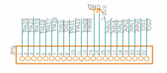
created a new sheet. First, I copied the pin head over from my motherboard, mirrored it (because I wanted the output board to be connected in
the inverse orientation), and added it. Then, I added the following components to my schematics:
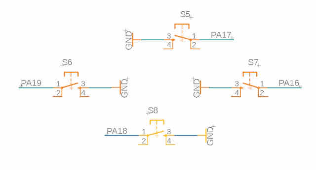
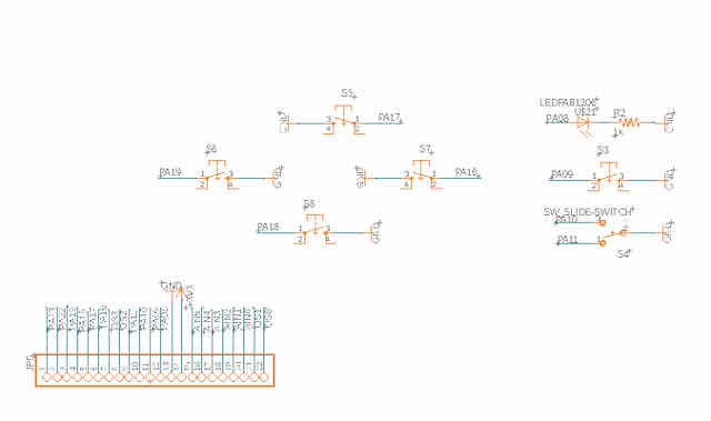
4x tactile switch (up, down, left, right): to navigate though a settings menu displayed on OLED screen
1x tactile switch: to take an image
1x slide switch: to switch between image capture and image review mode
1x red LED: to show status of current operation
1x 22x1 pin head: to connect to the motherboard (already copied from motherboard)
In total, I only had 7 digital pins to spare for my output board. This meant that I had to come up with a smarter way
of wiring my components than just giving all components their own pin. Furthermore, I remembered that the imaging sensor board
(which is connected to the same pins, just in the opposite direction) used 3 digital pins on its own when capturing an image. I
figured that I could re-use these pins for the take photo tactile button and the slide switch to switch between image capture and
image review mode, as long as I was ok with the fact that while the camera takes an image, these buttons could be used. This
sacrifice was acceptable for me (in fact, most DSLRs also don't allow you to do anything while an image is being captured).
I then used 4 of my 7 remaining pins for my 4 menu buttons and 1 pin for the red status LED, which left me with 2 more digital pins for the
OLED screen.
The inverted pin-header from the board last week
Wiring of the status LED, a capture button, and a slide switch. Note that I did not use any pull-up resistors, since the SAM D21E already has some built-in ones we can use programmatically
Wiring of my 4-button menu dial
A note about pull-up resistors for my buttons: You might be wondering why I did not use any pull-up resistors at my buttons, as
I used to do. After all, doesn't that mean that my button input will be floating when the button is not pressed? The SAMD21 actually has
built-in pull-up resistors, which we can use in our code by defining the type of the pin as INPUT_PULLUP. Therefore, I will not add
pull-up resistors for my buttons on the output board, but instead just route them directly from the respective pin to ground. There is one exception /
important consideration to this rule: As the use of the pull-up resistor on the pins is defined in software, in the case of a reset, this leaves
the pins floating on low impedence, before our setup code executes. This is not a problem for my menu buttons – but it could be a problem for my reset
button on the motherboard. This is the reason I added a large pull-up resistor to it on my motherboard, even though the reset pin has a small one already.
You can find more information about using these pull-up resistors here in the datasheet of the SAM D21.
A note about connecting my OLED screen: You might be wondering which pins I used to connect my OLED display. To understand the OLED display, I
first opened the datasheet of the SSD1306, which you can find here. As any OLED display, it uses
the SERCOM (=serial communication) SPI protocol. The protocol requires 4 pins to communicate data: a MOSI pin (=microcontroller output serial input pin), MISO pin (=microcontroller input serial output pin), SCK pin (=serial clock pin) and SS pin (=software-driven serial pin).
Now, when I first read these terms, I did not have any clue as to what this meant and whether or not I could just use any pins from my board. To cut it short: NO, you CANNOT use just any
pins for this. The SAM D21 datasheet lists the pins that can be used for SPI
under the chapter "IO/Multiplexing Considerations". A great and helpful guide to understanding this better can be found here.
If you want to dig deeper and understand the way the signal gets sent, I found this configuration guide to be of great help!
Another video that greatly summarizes it and puts the concept together on a SAM D21-based board is this one by Inventor Andy (embedded below):
An earlier version of my output board with a custom array of LEDs. I later replaced this simply with an OLED screen
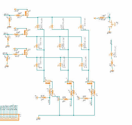
The finished schematics for my output board
Routing the Traces & Finishing my PCB Board
After arranging my board schematic, I switched to Eagle's PCB board tab and continued
by routing the traces of my PCB board. Again, roughly arranging the isolated parts of my board as I
did in my schematics helped me get to a possible physical layout quickly. I highly recommend this as a quick way
to get to an initial design that you can start working on. Although I first had some airwires
overlapping each other in my initial design, I could resolve all of these issues by changing the names of the pin wires my components were
wired to. You'll see some of the choices I made to make my routing as easy as possible in the screenshots below.
The final traces for my output board, with the drains connected row-wise and vias placed onto the footprints of the sources
After I had all my components routed in an efficient way, I added the outline of my
board. Although I did not nearly need as much space as I used in the end, I gave my output board the same dimensions as the input board I prepared last week by
copying the outline of that board. This is to make it easier to glue the two boards back to back. I then exported my final PCB traces and outline as two separate PNGs.
Again, I left the vias on both the traces and outline file to cut them through in my case. However, most people actually recommend exporting three separate files (traces, vias, outline).
A more complicated routing of the fixed resistors near the bottom of my board
A simpler routing of the same components
Finishing my PCB board by tracing the outline of my board
The final export of my traces (with vias) after editing in Photoshop
Milling & Stuffing the Board
After finishing and exporting both the traces and outline files into a format ready to cut, I went ahead and set up the endmill. I decided to use the Roland SRM-20 CNC machine
for cutting my PCB traces. I put a new copper plate
in the machine and firmly attached it to the sacrificial ground plate with double-sided tape (see this week on how to do this).
Next, I loaded my final PNG with the traces into Mods,
calculated the toolpaths with the default settings and for a 1/64 inch trace cut, and inserted the 1/64 endmill into the machine. All toolpaths looked well separated,
so I went ahead and started milling the traces. Afterwards, I used a 1/32 endmill and calculated the toolpath for an outline cut in Mods, which I subsequently cut.
Both milling jobs came out perfectly clean, with relatively wide traces and almost no copper splinters. I just quickly
washed the board under tab water with dish soap, let it dry, and felt ready to proceed to stuffing.
Milling the traces was smooth and at a similar depth all across the board
The final result came out very clean
I continued by soldering the components of my board, which took me about 30 minutes (again, this week's hardware is much easier). I only permanently mounted the buttons and the LED; the
OLED screen was attached just by soldering on some pin-heads onto the board for the connections of my OLED screen. This not only enabled me to exchange the OLED screen, should it not work
as expected, but also potentially upgrade it to a bigger screen later. I highly recommend using pin-heads for whole isolated component boards like these (I have to remind myself about that).
Soldering the front side of my PCB board
Soldering the back side of my PCB board with jumper wires
Programming & Testing the OLED Screen & Menu Buttons
Alight, this part is the core of my work this week. As I have never worked with OLED screens, I first dove into understanding how these
screens work and which libraries I needed to control them. My output board is designed to be used together with the motherboard I produced two weeks ago and the
input sensor from last week. The motherboard already had a bootloader installed and was already programmed with a
simple blink script to blink its on-board LED. I connected the imgae sensor and the output board to my motherboard by sliding the two 22x1 pins into the respective holes on my motherboard.
The connections were not soldered at this point, though I was confident that the boards were sufficiently connected for testing and debugging. I hooked up my
motherboard via its micro-USB port to my Macbook again and opened Arduino IDE. Then, I used the same simple script from last week to cycle through all transistors and read
their values. However, this time, instead of writing them straight into the console, I constructed an array of pixels on the OLED screen and output their values as a grey-scale pixel from 0 to 255.
Hooking up my output board to the motherboard and programming the motherbard
Implementing the logic to read out individual pixels and print an image on the OLED screen
I tested and refined my script and used a phone flashlight and a laser pointer to test the phototransistors individually. Luckily, they were all soldered on
correctly, and I could read out a valid signal from them. So far, we can only capture an image in an automated way and view it through serial communication to the OLED screen.
Time to code the code for the buttons to interface the camera. This is where it will all come together!
Using the motherboard-image-sensor-OLED-screen complex as a "standalone" camera with the LiPo battery!
After a ton of code-debugging (without yielding any useful learnings, other than that I should probably not have coded this script at 2am in the morning), the
board finally produced images that could be viewed on the OLED screen! Moreover, I could use the switch button to see the last captured image. Although I wanted to
code a menu to control the exposure settings before taking an exposure, I ran out of time for this feature this week. Therefore, this will be part of next week's
upgrade where I plan to finish the camera with some added bluetooth-capabilities to send captured images to my smartphone. Stay tuned!
I had the privilege to be a student in Neil Gershenfeld's MAS.861: How to Make (Almost) Anything in Fall 2022. His class is a digital fabrication masterclass that requires rapid prototyping (and leads to frequent failure). All the projects you can find on this website – as well as this website itself – were built from scratch where feasible. Explore other projects or take the class yourself from any maker space around the world through FabAcademy.