

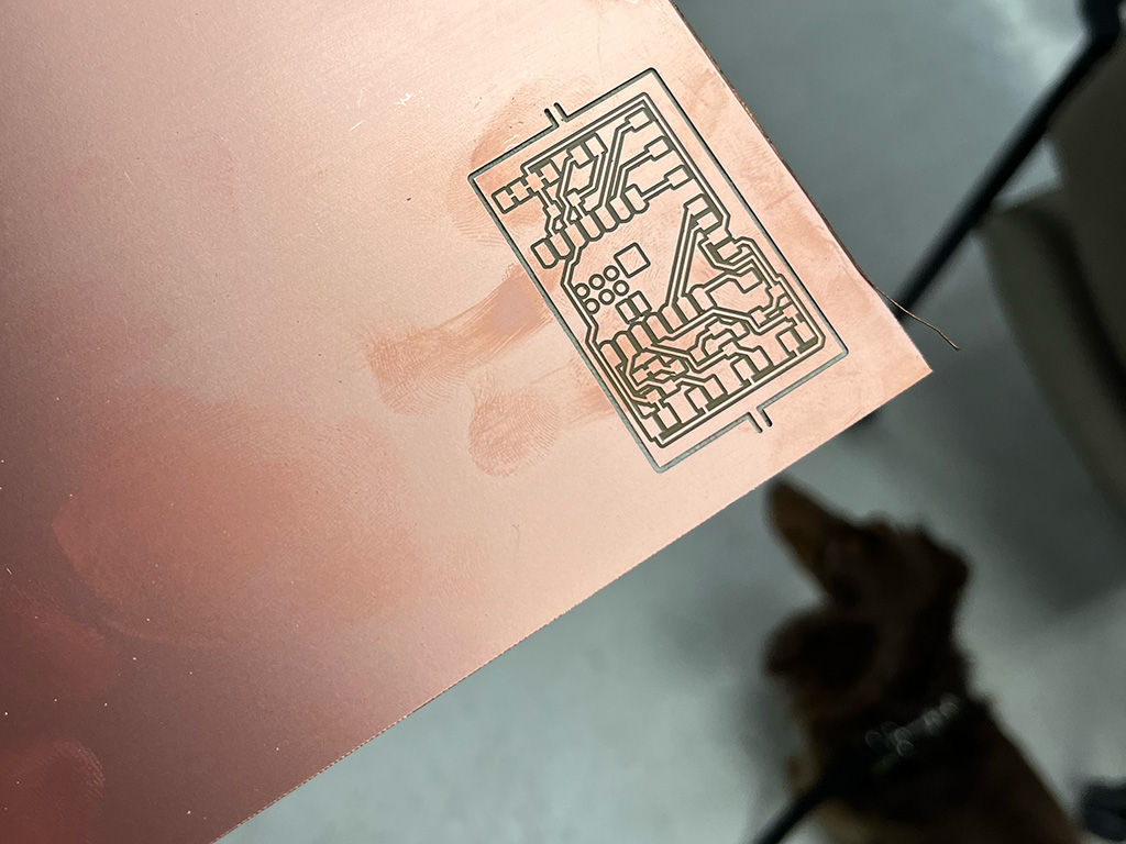
Our group met with Quentin and he walked us through the workflow of sending out a PCB for fabrication using JLPCB and the various options they have for that. He talked about materials, solder masking, and stencils among other things. Then showed us how to use the milling machine for in-house fabrication. He wrote a program that makes using the already very user-friendly machine even easier- as in you pretty much just have to upload your files and the program formats them for you. We milled this to examine the design rules for the machine:
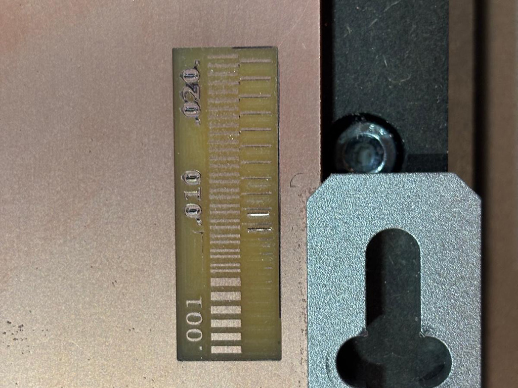
When I designed my board last week, I forgot to change the settings to account for the above and my design was super intricate, so I basically had to rework the entire thing. I also added a 5th analog input. Here's what I came up with:
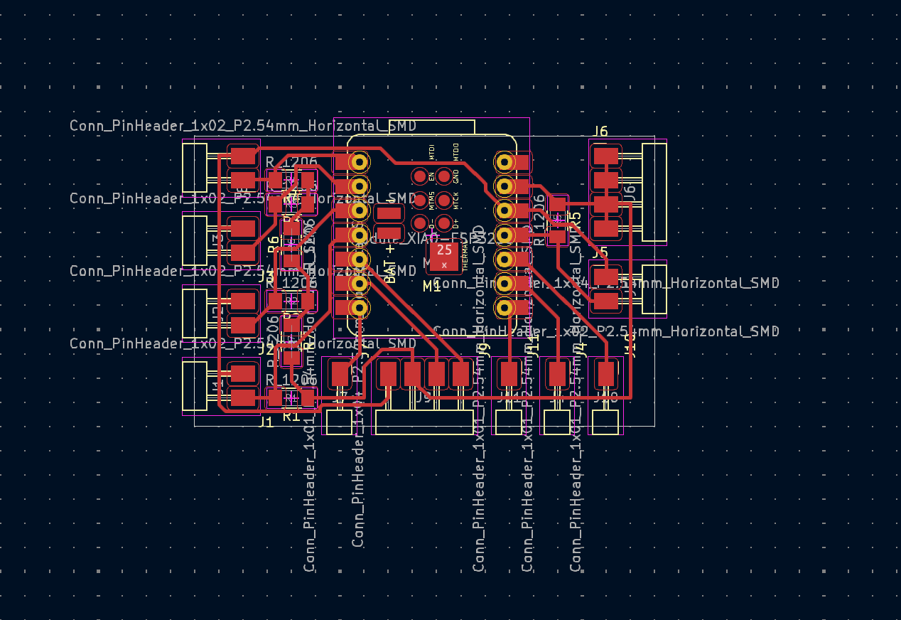
This was maybe the 4th? iteration of me having to tweak things because getting things to line up and be super compact was tough and then the milling path preview generated by mods wasnt looking right. But eventually, using Quentin's gerber2img converter I was able to make these two pngs from the gerber file for the traces and the edge cut, and then turn those into a g-code file for the machine and see the preview using mods (that process also took some troubleshooting to get working right-- mods is super easy to use but getting the pngs aligned and also just getting my design right took a few tries).
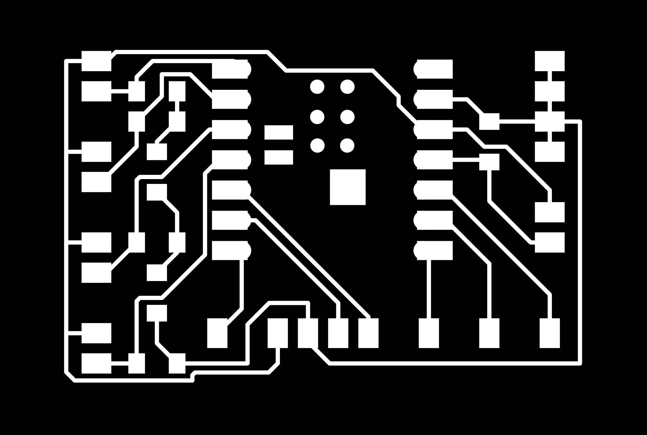

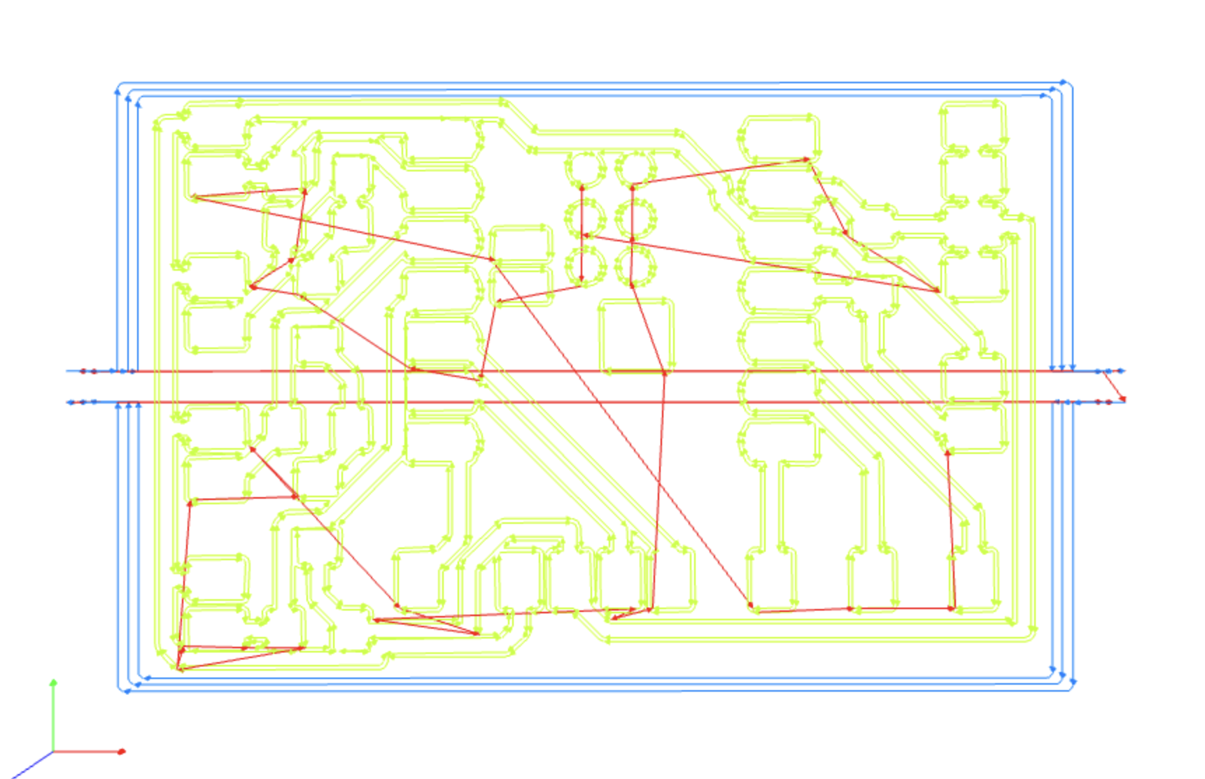
After that I was finally able to mill my board!
And then I had to solder it. It was looking pretty messy at first because rather than surface mount the xiao, I wanted to use headers so I could remove and reuse it, and hacking together a solution to get the headers to sit well on top of the pads was a bit tough and also just tough to solder because there was so little room to work with. But I finally got the hang of it and it was going smoothly! Until I stupidly tried to bend a row of soldered on pins and ripped off an entire side's worth of pads. Oof.
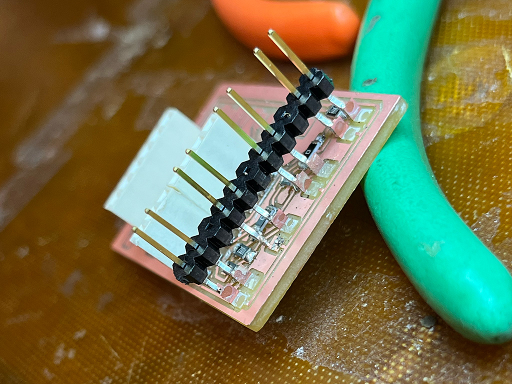
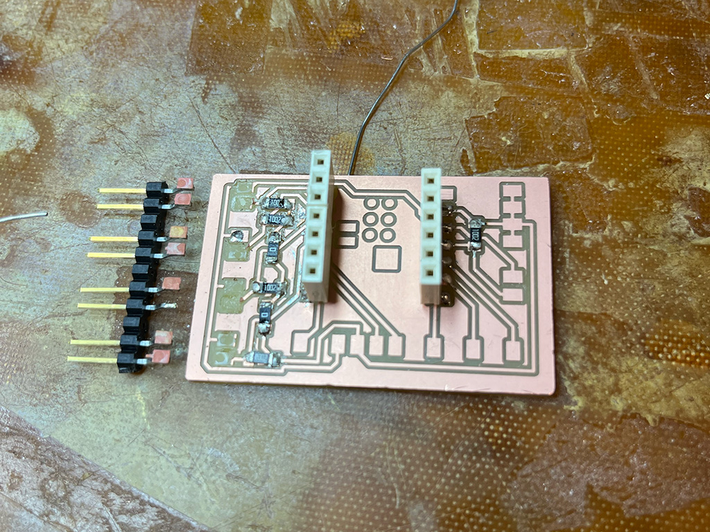
Honestly I was in the zone and not too bummed because I saw this as an opportunity to do a cleaner solder job on my next attempt and since I'd already uploaded my file to the milling machine it was super easy to run again. I chose a slightly different material with shinier copper because it was stacked alongside the rest and looked cooler and I didn't think it would be any different. Turns out the copper facing was flimsier, didn't mill as cleanly, and started peeling off (and some traces just broke) easily when I was soldering it. So I milled yet another. And it finally worked out. There were no more 10k resistors left so I had to get them off the first attempt board which was annoying but not too bad. I also tried to attach the pins at a more secure angle. And here she is!
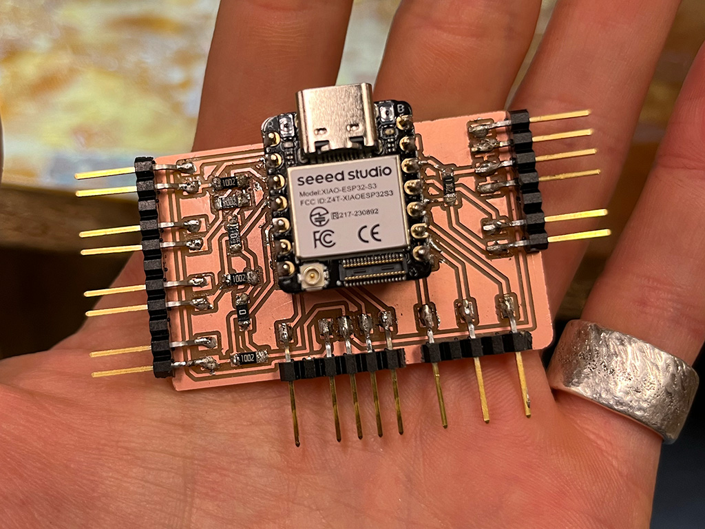
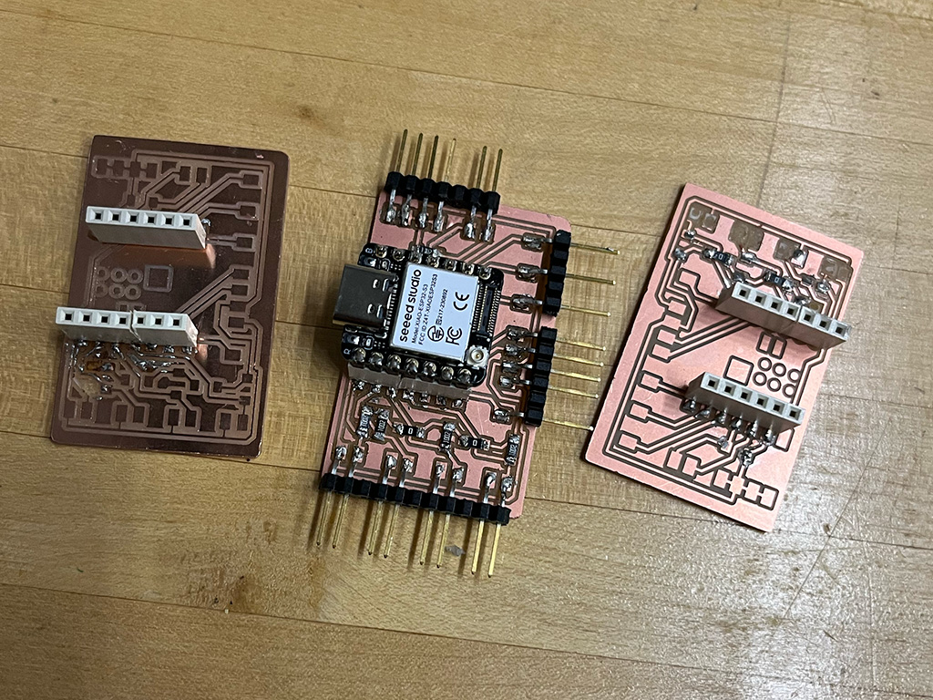
I haven't tried to upload any code yet but I did use a multimeter to test all of my connections and it looks good!
When I ran out of time during week 6 for testing, my plan was to test this board during inputs week and report back here. But by the time that rolled around, my needs changed and after milling 2 new boards, I ended up with one that worked and suited my needs for input/output testing. Everything on the board works as expected, and the process of making it, as well as testing the inputs is documented on my week 8 assignment. To see the on board LEDs in action, check out week 9. At this point, making dev boards is my strongest skill I've learned in the class just from how many times I've failed, broken something, or just changed course and needed to redo things...
-- Gcode used to mill the board
-- PNGs used to make the gcode