
Week 5
Electronics Production
Week Highlights
This week focuses on electronics production, covering PCB fabrication techniques, assembly processes, and creating functional embedded microcontroller systems. We explore both in-house production methods and board house services.
PCB Milling Design Rules
Characterize design rules for in-house production
Double-Sided PCB Success

Functional double-sided PCB with toddler-friendly interface
Board House
Submit PCB to board house for production
Table of Contents
Course Content
Production Methods
Assignments & Projects
Electronics Production
This week covers the practical aspects of electronics production, including PCB fabrication methods, assembly techniques, and creating functional embedded microcontroller systems. We explore both in-house production capabilities and board house services.
This Week's Goals
- Characterize PCB production process
Test design rules for in-house PCB fabrication and understand limitations - Design and fabricate embedded system
Create custom microcontroller board and test functionality - Submit to board house
Learn boardhouse PCB production workflow and design rules
Assignments
- Group Assignment
Characterize design rules for in-house PCB production process; submit PCB design to board house - Individual Assignment
Make and test embedded microcontroller system; extra credit for alternative process
Tools & Materials
- PCB Materials — FR4, FR1, Kapton, copper foils
- Fabrication Tools — CNC mill, etching chemicals, drill bits
- Assembly Tools — Soldering iron, microscope, flux, solder
- Testing Equipment — Multimeter, oscilloscope, power supply
PCB Fabrication Methods
Understanding different approaches to PCB production, from traditional etching to modern machining and boardhouse services.
In-House Methods
- Etching — Ferric/cupric chloride, ammonium persulfate
- Machining — CNC milling with 1/64", 1/32", V-bits
- Vinyl Cutter — Flex connections and encapsulation
- Laser Engraving — Combined LIG processes
Boardhouse Services
- Board Houses — JLCPCB, PCBWay, OSH Park
- Design Rules — 15/5 mil width/spacing
- Layers — 1, 2, 4+ layer options
- Assembly — Pick-and-place, reflow soldering
Assembly & Soldering
Essential techniques for assembling and soldering electronic components, from through-hole to surface-mount devices.
Soldering Techniques
- Manual Soldering — Iron station, fume extractor, microscope
- Reflow Soldering — Hot plate, convection oven, IR
- Hot Air — For SMD components and rework
- Wave Soldering — For through-hole components
Component Types
- Through-Hole — Traditional components with leads
- Surface-Mount — SMD components, smaller footprint
- Chip-Scale — BGA, QFN, CSP packages
- Headers — Connectors and interface components
Board House Services
Boardhouse PCB production services offer higher precision, better quality, and advanced features compared to in-house methods.
Popular Board Houses
- JLCPCB — Low-cost, fast turnaround, good for prototypes
- PCBWay — Professional quality, assembly services available
- OSH Park — Open source friendly, purple soldermask
- Aisler — European service, good for EU projects
Debugging & Testing
Systematic approach to troubleshooting and verifying electronic systems functionality.
Debugging Checklist
- Inspect and reflow solder joints
- Check component orientation and values
- Verify datasheet specifications
- Confirm connector orientation
- Measure supply voltages
- Probe I/O signals with oscilloscope
Training
Essential training materials and procedures for PCB milling using the Othermill machine.
Standard Operating Procedure (SOP)
Equipment Specifications
Pre-Processing
- Power on the machine using the rear power button
- Initialize homing sequence through Bantam Tools software
- Load design file: Export from Fusion as .brd (Eagle 9.x compatible) or generate Gerber files from fabrication outputs
- Configure hole types: Click PTH first; NPTH (non-plated through holes) requires edge cuts for proper origin alignment - process in second mill unless using vias for rivets
Workpiece Setup
- Activate loading sequence to position machine at front
- Remove magnetic panels and prepare workpiece area
- Apply double-sided tape across entire board surface
- Position board left-justified with 1mm buffer from origin
- Set Z-offset 5mm from origin point
Tool Configuration
- Add 1/64" end mill as secondary tool in tool list
- Install tool by aligning end mill shoulder with collar
- Select appropriate tool size and confirm installation
Milling Operation
- Install acrylic safety panels (required for operation)
- Verify hall effect sensor detects magnetic panel closure
- Execute "Mill All Visible" command to begin fabrication
- Monitor process completion (estimated 14 minutes to 2 hours)
Post-Processing
- Retract machine using loading controls
- Remove completed board from work area
- Clean debris using CleanView Deluxe vacuum system
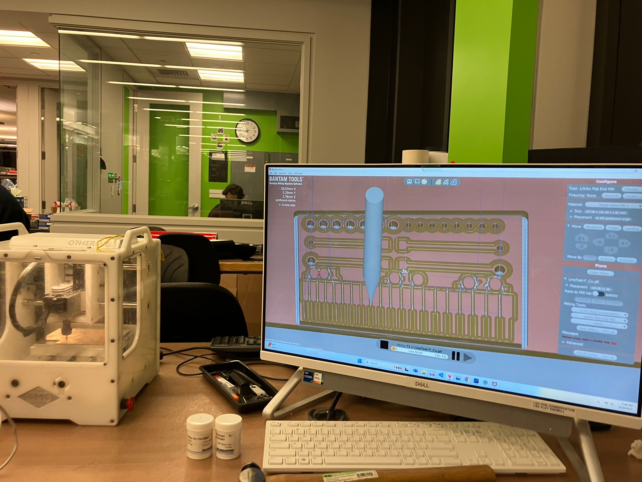
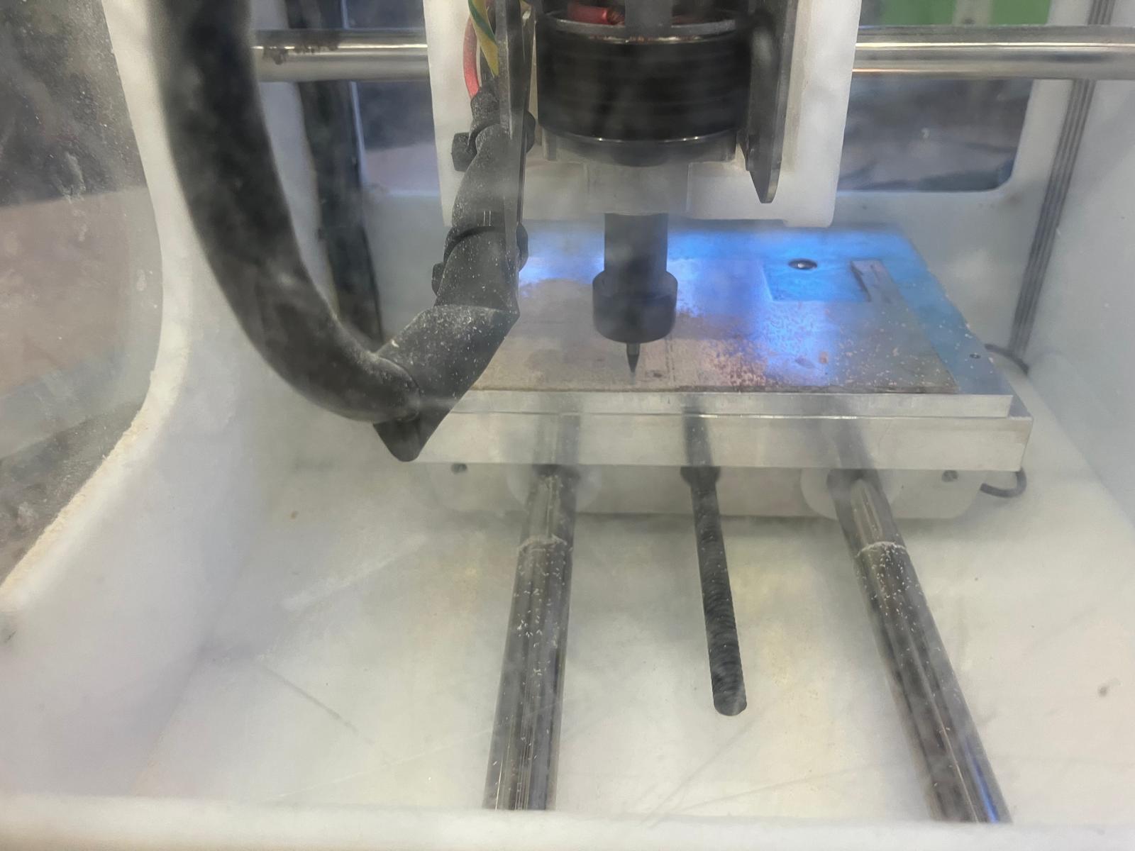
PCB milling process using the Othermill machine
Double-Sided Milling
Process for creating double-sided PCBs using the Othermill machine with fixture installation and proper alignment techniques.
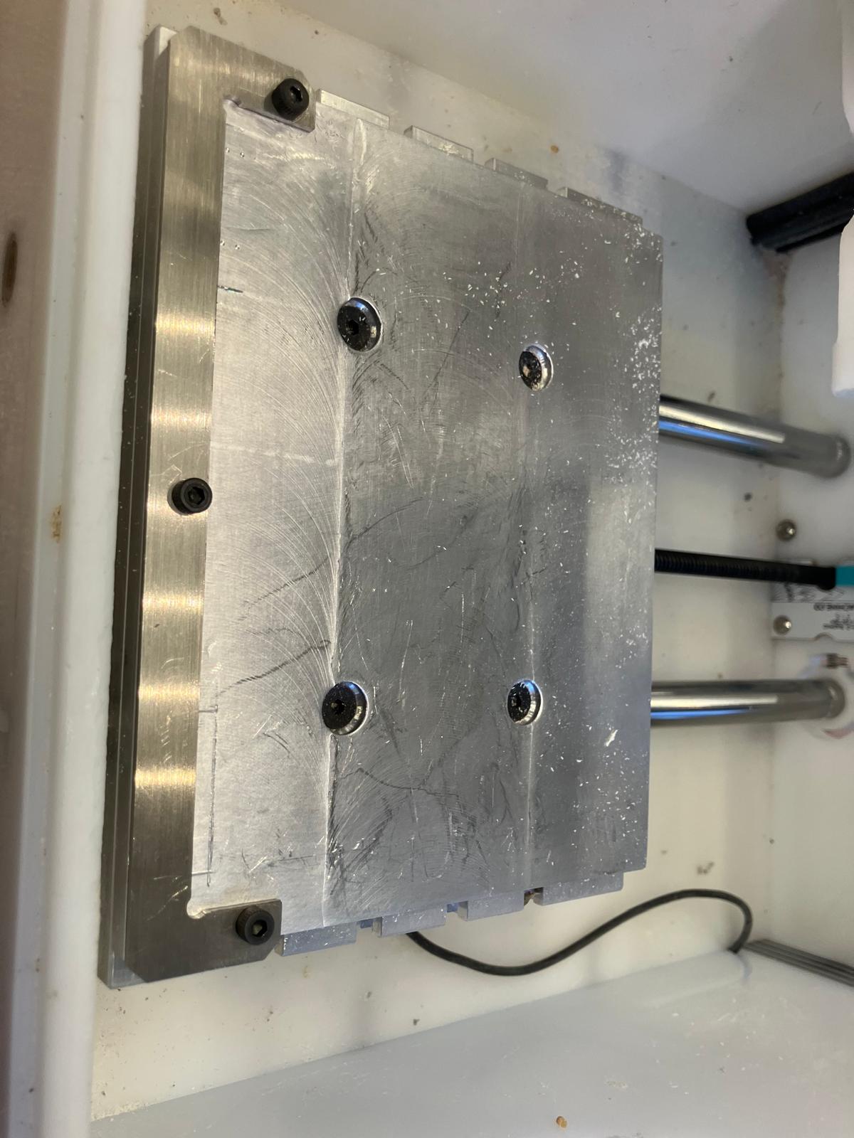
Double-sided fixture bracket installation for precise board alignment and milling
- Software Configuration: Select double-sided mill option in the software interface
- Fixture Installation: Add fixture under Fixture menu and follow installation steps using Allen wrench
- Top Side Setup: Align base material to bottom left corner, run workflow for top setting (click outline to shade out cut-out traces)
- Board Flip: Flip the board left to right upside down for bottom side processing
- Bottom Side Setup: Align board to bottom right corner, run same workflow for bottom setting (click outline again to cut out border traces)
Installing Rivets
Critical process for installing copper rivets to create electrical connections between board layers in double-sided designs.
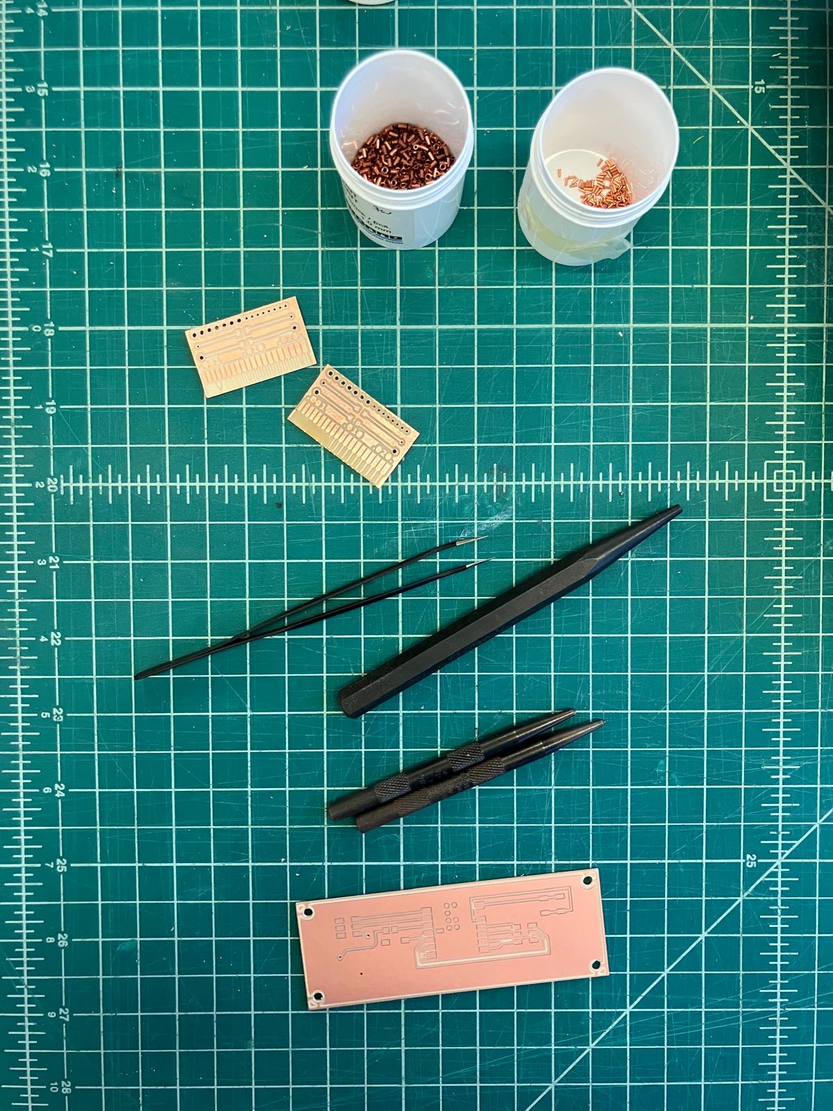
Copper rivets used for creating electrical connections between board layers
⚠️ Important Safety Note
Handle rivets carefully - there are thousands available but they are relatively expensive. Avoid spilling them during the installation process.
- Rivet Placement: Use tweezers to carefully place rivets in the vias
- Board Flip: Flip the board without dropping it to access the opposite side
- Small Conic Tool: Use the small conic tool inside the rivet (on opposite side) and lightly hammer to open and secure it
- Large Conic Tool: Use the large conic tool on the rivet and lightly hammer to flatten it on the surface
- Soldering: Add solder when soldering to secure the connections between rivet and board copper
Reference Materials
Source: Original hand-typed training notes
Detailed training notes from MIT HTMAA Slack channel with comprehensive SOP and pro tips
Pro Tips & Best Practices
Design Optimization
- Single-sided boards: Prefer zero-ohm resistors over double-sided designs when possible
- Flexible alternatives: Consider vinyl cutter for translucent board applications
- Feature control: Toggle traces, holes, and outlines independently for selective milling
Workflow Efficiency
- Tool management: Store wrenches on machine tip; use left hand for small wrench operations
- Time estimation: Short jobs ~14 minutes, long jobs ~2 hours (automatic tool switching not available)
- Process monitoring: Time estimates are approximate; monitor progress manually
Advanced Techniques
- Solder resist: UV-cure solder resist available (process development ongoing with lab staff)
- Rivet alternatives: Avoid copper rivets (1mm/0.6mm sizes) - complex installation requiring conical hammering and dual-side soldering
Group Assignment
Characterize the design rules for in-house PCB production process and submit a PCB design to a board house.
Part 0: Design Rule Test Pattern
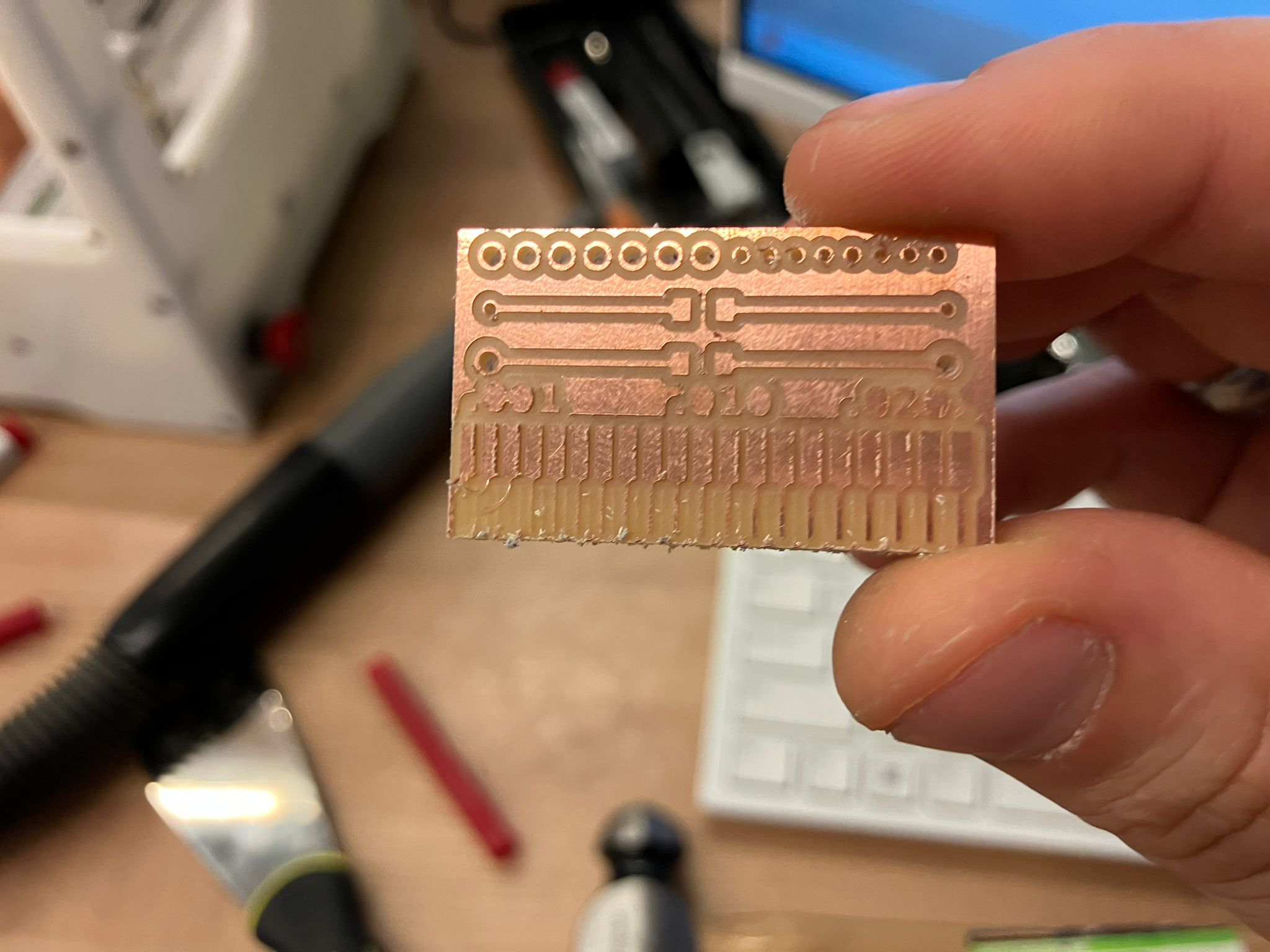
Comprehensive PCB design rule test pattern created to characterize in-house production capabilities and validate design constraints for successful fabrication.
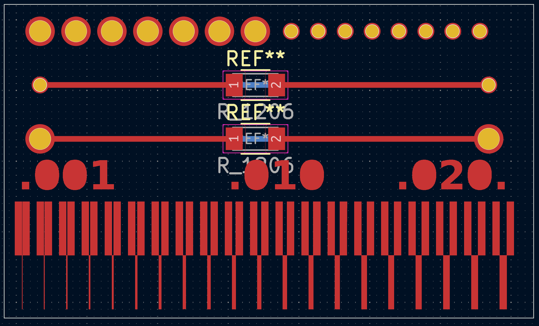
Design rule test pattern showing trace widths, spacing tolerances, and hole sizes for characterization
Design Files
KiCad PCB: Complete PCB design file with test patterns and design rules.
Gerber Files: Front copper layer, edge cuts, and drill holes for PCB fabrication.
Part 1: Design Rule Characterization
Comprehensive testing of in-house PCB production capabilities through systematic evaluation of trace widths, spacing tolerances, and mechanical durability.
Characterized Design Rules
4 mil (0.004") pre-test
9 mil (0.009") post-durability test
16 mil (0.016") minimum
Based on 1/64" tool width
Note: Design rules are guidelines; actual tolerances may vary based on material and process conditions
Durability Testing Results
Pre-test: Initial trace pattern
Post-test: Surviving traces after mechanical stress
Part 2: Boardhouse Submission
Evaluation of boardhouse PCB manufacturing services through JLCPCB submission to compare design rules, pricing, and production capabilities with in-house methods.
JLCPCB Submission Workflow
- Access JLCPCB online platform and create account
- Upload PCB design files (Gerber format)
- Select aluminum substrate (preferred over FR4 for machining compatibility)
- Configure production parameters and place order
JLCPCB Order Documentation

JLCPCB order confirmation showing PCB specifications, pricing, and production parameters
PCB Simulation Results


Detected 2 layer board of 100x100mm(3.94x3.94 inches).
Order Documentation
PCB Specifications: Detailed technical specifications, design rules, and manufacturing parameters for the PCB order.
Order Checkout: Complete order details including pricing breakdown, shipping options, and payment confirmation.
Production Specifications
1.6 mm (standard)
Multiple colors (adds processing time)
Various options available
Individual Assignment
Make and test an embedded microcontroller system that you designed, with extra credit for using an alternative production process.
Project Overview
Design and fabricate custom embedded microcontroller systems using single-sided PCB milling techniques, focusing on ESP32-S3 based development boards with comprehensive testing protocols.
Development Sequence
- Phase 1: ESP32-S3 LED PCB - Basic microcontroller board with LED control
- Phase 2: ESP32-S3 LED Connector PCB - Enhanced version with additional connectivity
Functional Testing Protocol
Load Cell Integration
- Interface with load cell and amplifier board
- Design two-layer PCB with compatible header connections
- Develop data acquisition and processing code
Accelerometer Network
- Integrate accelerometer sensor module
- Establish wireless communication between ESP32-S3 nodes
- Implement data tethering and synchronization protocols
Advanced Manufacturing Exploration
Laser Cutter Application
Develop origami-style PCB design that mechanically activates LED through folding mechanism
Vinyl Cutter Application
Create flexible PCB using copper ring material for accelerometer integration
Successes and Failures
Key challenges encountered during FR1 soldering and solutions developed through experimentation and peer collaboration.
| Problem | Solution | Source |
|---|---|---|
| Can't heat for too long otherwise you burn off the copper | Preheating helped with flame retardant boards, but doesn't work with FR1 | Personal experience |
| Can't use too much solder, otherwise it flies off onto other parts | Extra solder bunches up on flame retardant boards, but FR1 requires precise control | Personal experience |
| Poor solder sticking to copper grooves | Careful sand papering for the grooves to help with solder sticking | Omar Aldajani (previous HTMAA student) |
| Poor thermal transfer and solder adhesion | Using flux on the copper for better thermal transfer and solder sticking | Omar Aldajani (previous HTMAA student) |
| Extra solder on copper is annoying and hard to remove | Add more solder and remove it again, or carve away some copper so the short doesn't matter | Anthony (lab instructor) |
Reference Materials
Source: MIT HTMAA Slack Discussion
Additional insights and peer collaboration on FR1 soldering challenges and solutions
Project Documentation
Initial PCB milling design showing early layout and trace patterns
Final successful PCB milling result with clean traces and proper spacing
Successfully assembled Xiao ESP32-S3 microcontroller board with LED functionality
Diode testing failure highlighting soldering challenges and component orientation issues
Summary
FR1 soldering presents unique challenges compared to flame retardant boards, requiring precise heat control and solder management. Through peer collaboration and systematic problem-solving, effective techniques were developed including careful sanding, flux application, and strategic solder removal methods.
Remilling and Soldering After Copper Solder Insights
After gathering copper solder insights from peer collaboration and lab experience, I prepared all necessary components and tools for assembly. With boards ready, solder wick prepared, and pen flux available, I proceeded with the soldering process.
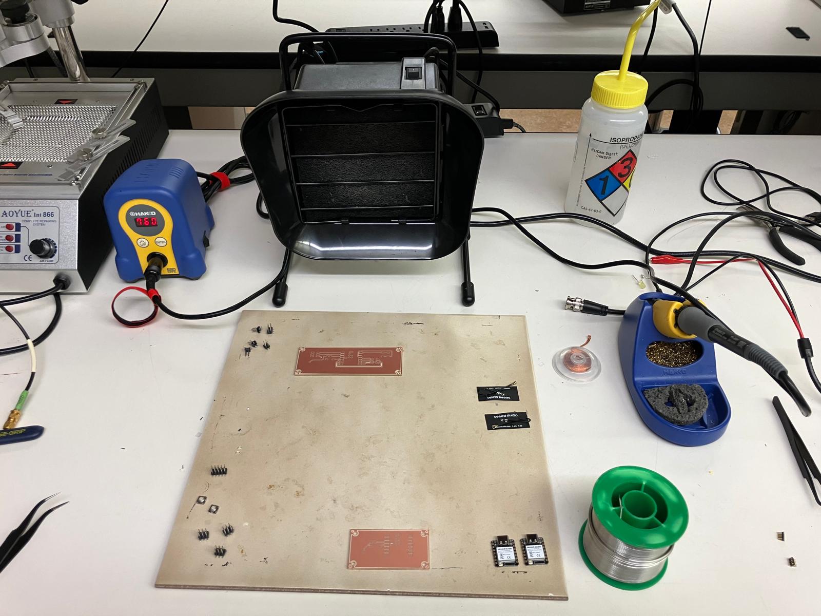
Complete soldering setup showing boards, components, solder wick, and pen flux ready for assembly
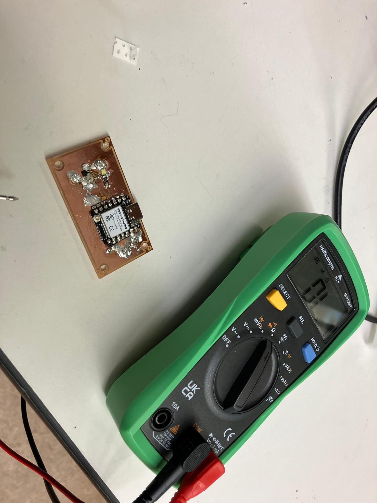
Following soldering, I conducted comprehensive testing including resistivity measurements, diode tests, and continuity tests to diagnose and resolve minor issues. This systematic approach helped identify and fix problems such as additional solder needed from rivet to board connections and removing shorts (e.g., 10k resistor bridges).
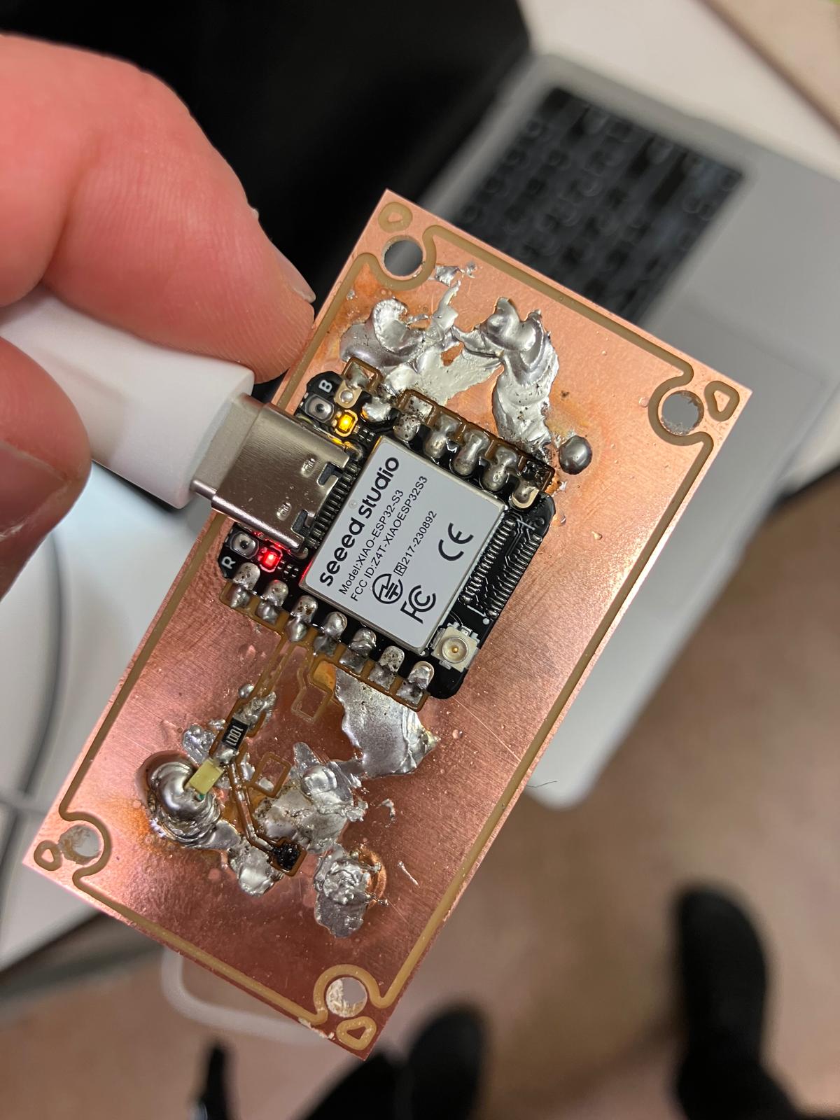
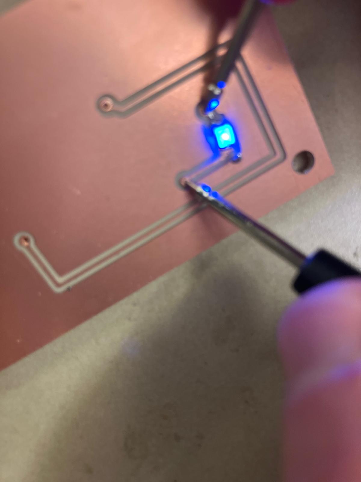
Front LED Diode Works on Base Dev Board Design
The front LED functionality was successfully implemented on the base development board design. However, the button remains shorted despite multiple troubleshooting attempts including solder wicking and microscopic inspection for bridges.
Front LED diode test demonstrating successful LED functionality on base development board
Base LED development board successfully programmed and operational with LED control functionality
The board functions correctly without the button, and the LED has been successfully programmed. The button shorting issue continues to be investigated, as standard troubleshooting methods have not yet resolved the problem.
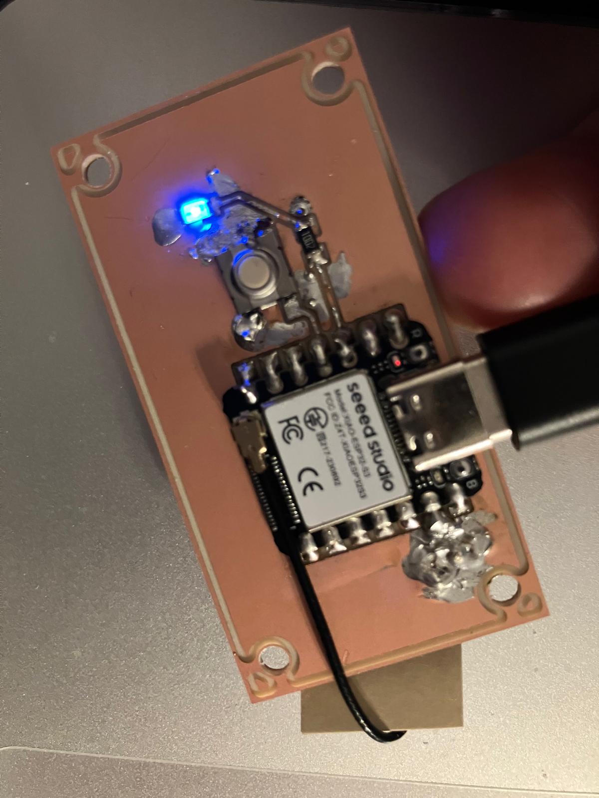
Back LED Works on Connector Dev Board Design with Full Pinout
After practicing with two base LED development board soldering attempts, this fabrication process proceeded smoothly with all components functioning correctly, including the button. The systematic approach of verifying button lead connections before and after pressing, both before and after soldering, proved essential for success. This design uses the ESP32-S3 LED Connector v6 design.
Back LED diode test showing successful functionality on the connector development board design
Double-sided development board demonstration showing full functionality with LED control and button operation
Animated demonstration of the double-sided development board in operation with LED and button functionality
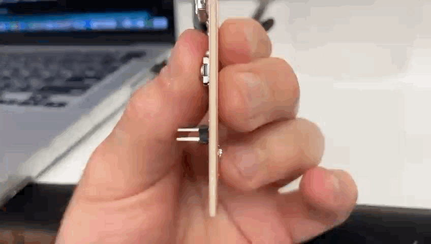
Toddler-friendly button test demonstrating the interface's usability and reliability for young users
Success! The double-sided development board for ESP32-S3 with LED on the back is fully functional. The board passed comprehensive testing including the toddler-friendly interface test. With the LED successfully implemented on the back, substantial real estate is available for additional components such as four buttons and a screen for reaction time and other prototype applications.
Design Note: For one USB-C cable, I needed to trim the connector edge because the microcontroller is positioned further into the board. I found a thinner cable that connects without modification. In future design iterations, it would be beneficial to redesign the board to position the microcontroller closer to the edge, maintaining the same distance as the base LED design for improved accessibility.
Dev Board Testing
I set up a Seeed XIAO ESP32-S3 with an MPU6050 accelerometer, HX711 load cell amplifier, and SSD1306 OLED display, all sharing 3.3V power. The OLED never displayed anything, and both the sensors and display returned repeated I²C timeout errors. I corrected power from 5V to 3.3V, verified wiring, and confirmed that SDA = GPIO 5 (A4) and SCL = GPIO 6 (A5), but the I²C scanner still detected no devices. The MPU6050 powers on, yet no readings appear in the Serial Monitor. The load cell connects and gives intermittent readings, requiring improved connections in future iterations towards the final project.
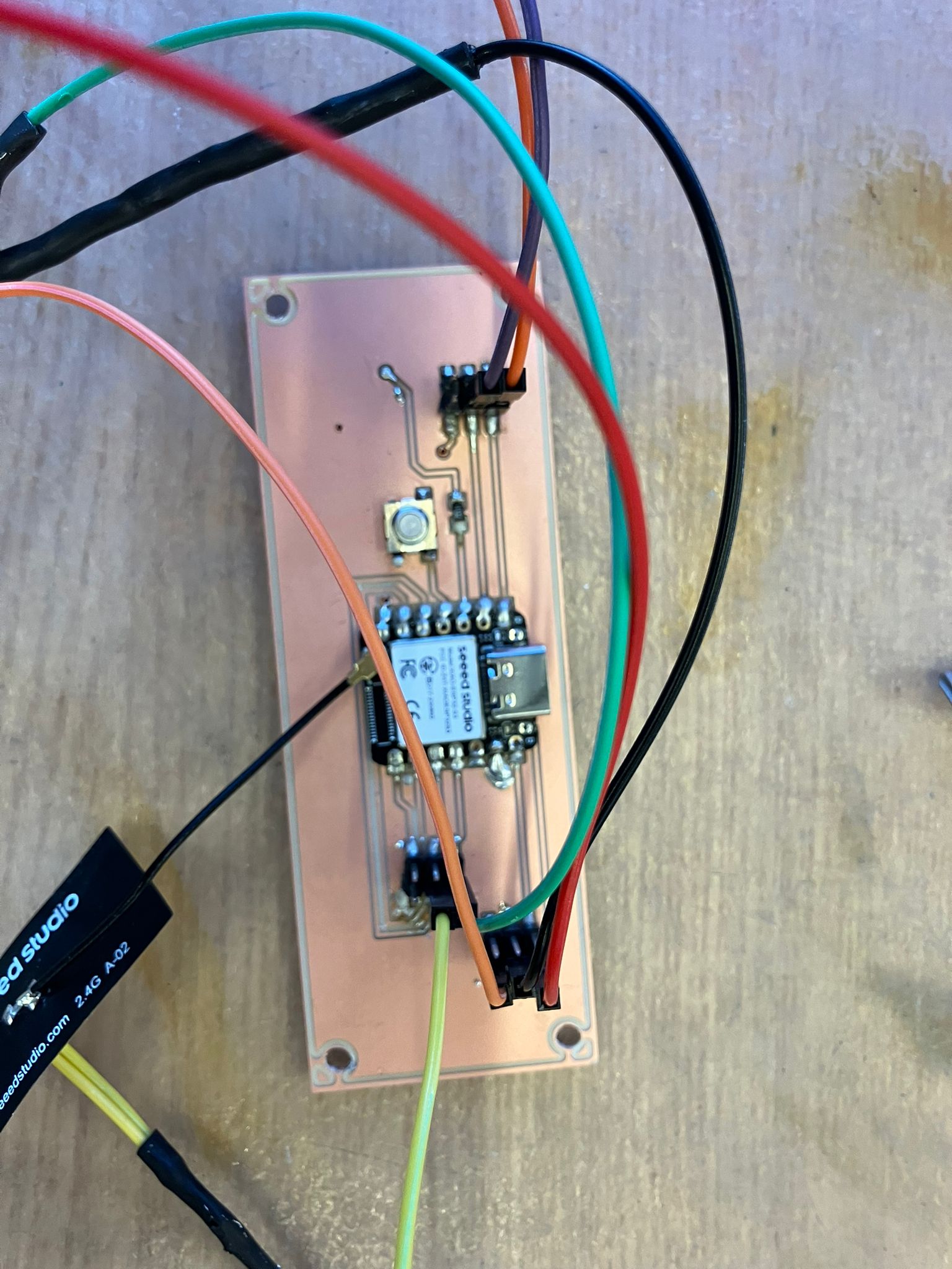
Development board setup with MPU6050 accelerometer, HX711 load cell, and SSD1306 OLED display
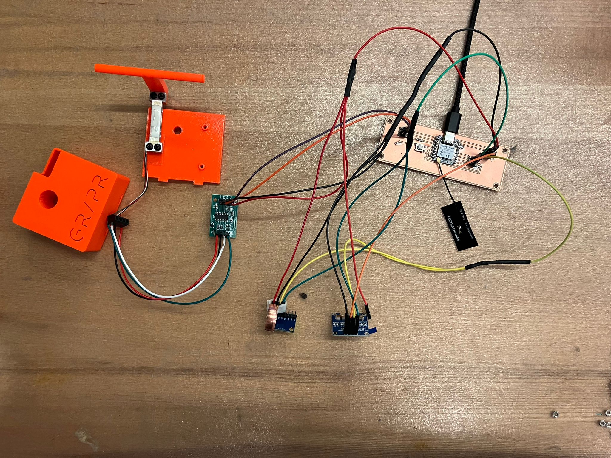
Complete development board configuration showing all sensor connections and power distribution
Component Pinout Configuration
| Component | VCC | GND | SDA | SCL | Other Pins |
|---|---|---|---|---|---|
| MPU6050 | 5 or 3.3V | GND | A4 (GPIO 5) | A5 (GPIO 6) | — |
| OLED (SSD1306) | 5 or 3.3V | GND | A4 (GPIO 5) | A5 (GPIO 6) | — |
| HX711 + Load Cell | 5V | GND | A0 (DT) | A1 (SCK) | Logic 3.3V-safe |
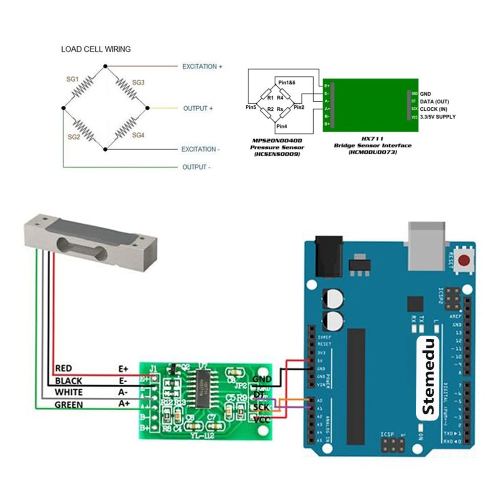
HX711 load cell amplifier board pinout configuration (Amazon product page)
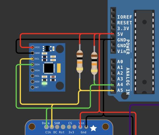
MPU6050 accelerometer pinout diagram (Wokwi simulation reference)
Troubleshooting Results
Issue 1: I²C Communication Failure
SDA and SCL were shorted to ground, suspected connector or XIAO board. After removing connector, the short persisted, indicating the XIAO board itself was the issue. The accelerometer still powered on despite the communication failure.
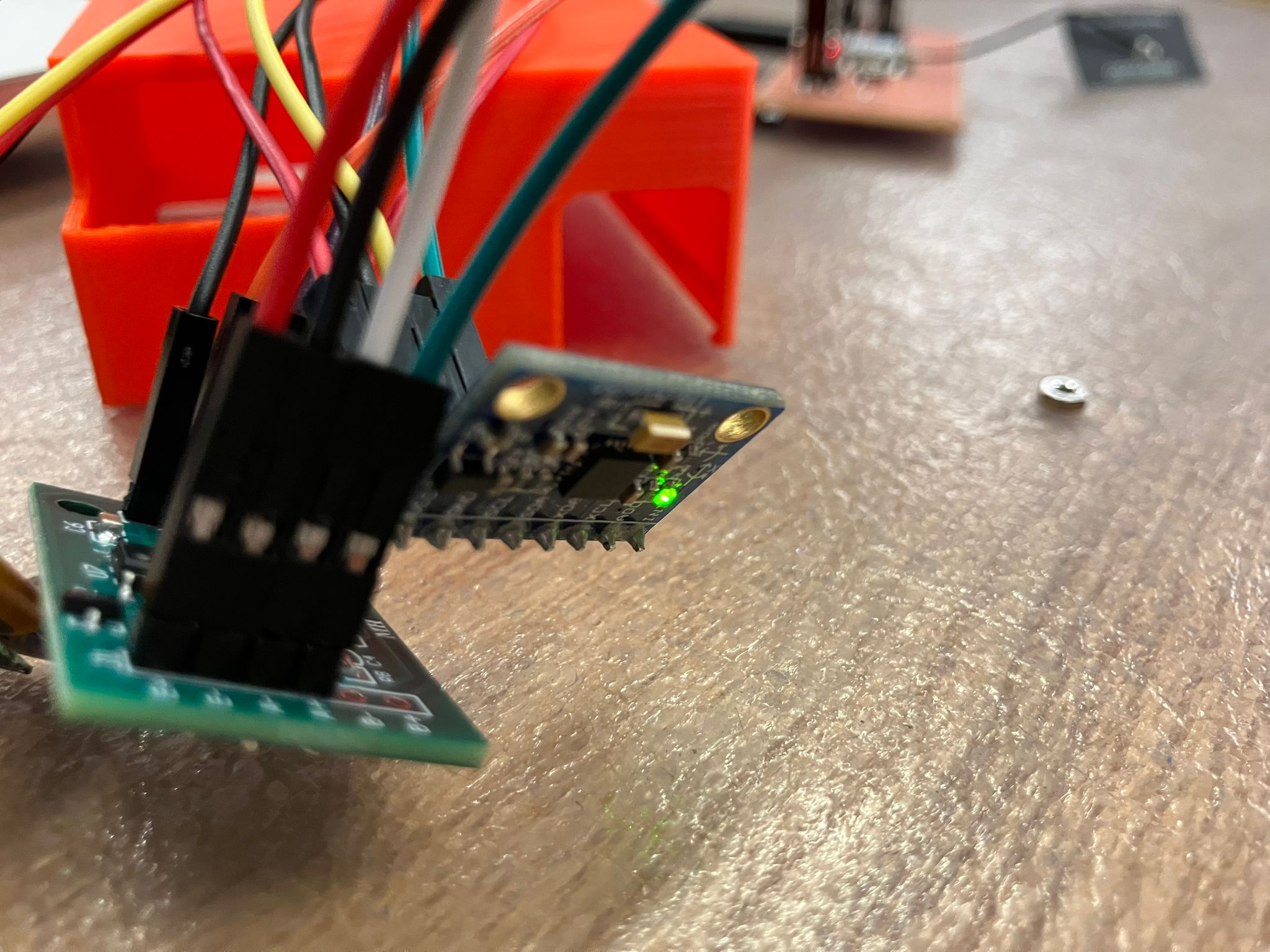
MPU6050 accelerometer showing power indication despite I²C communication issues
Issue 2: Load Cell Connection Problems
The load cell had intermittent connection issues but still provided some readings. Since it uses analog outputs, I was able to capture several data points for analysis.
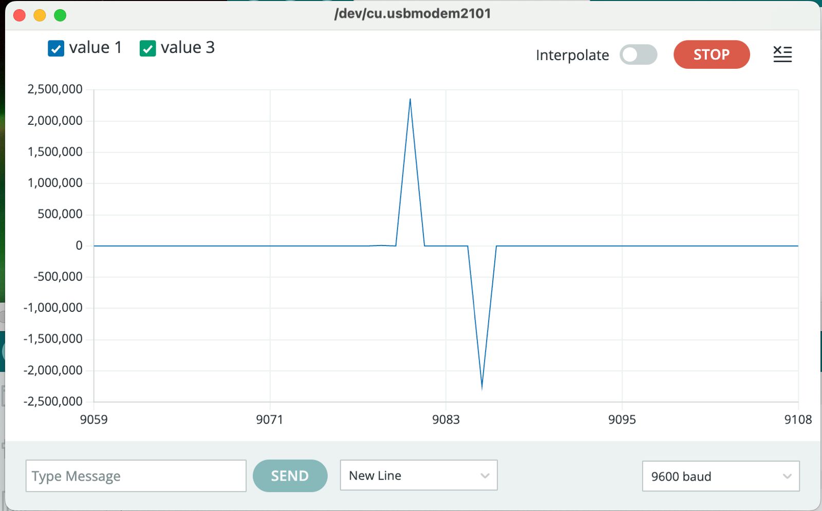
Serial plotter showing load cell data visualization
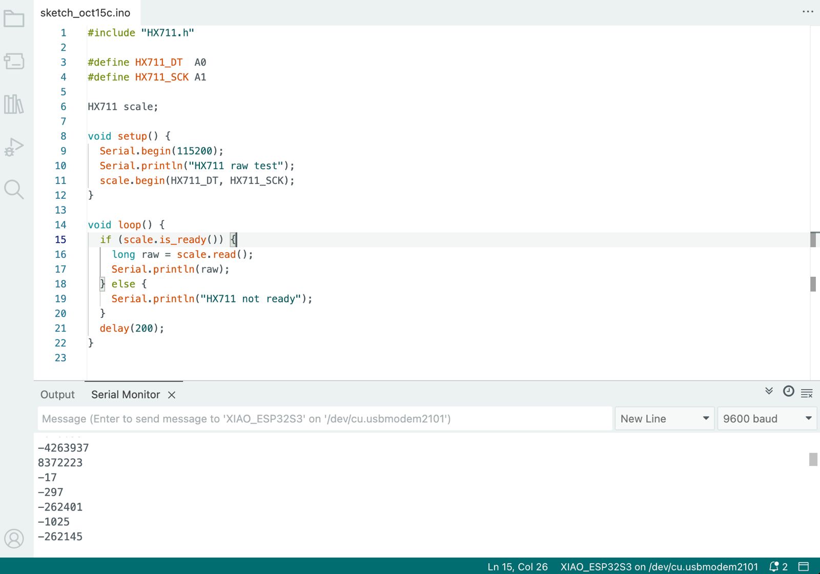
Serial monitor displaying load cell readings and status
Additional serial monitor output showing load cell data patterns
Dev Board Development Process
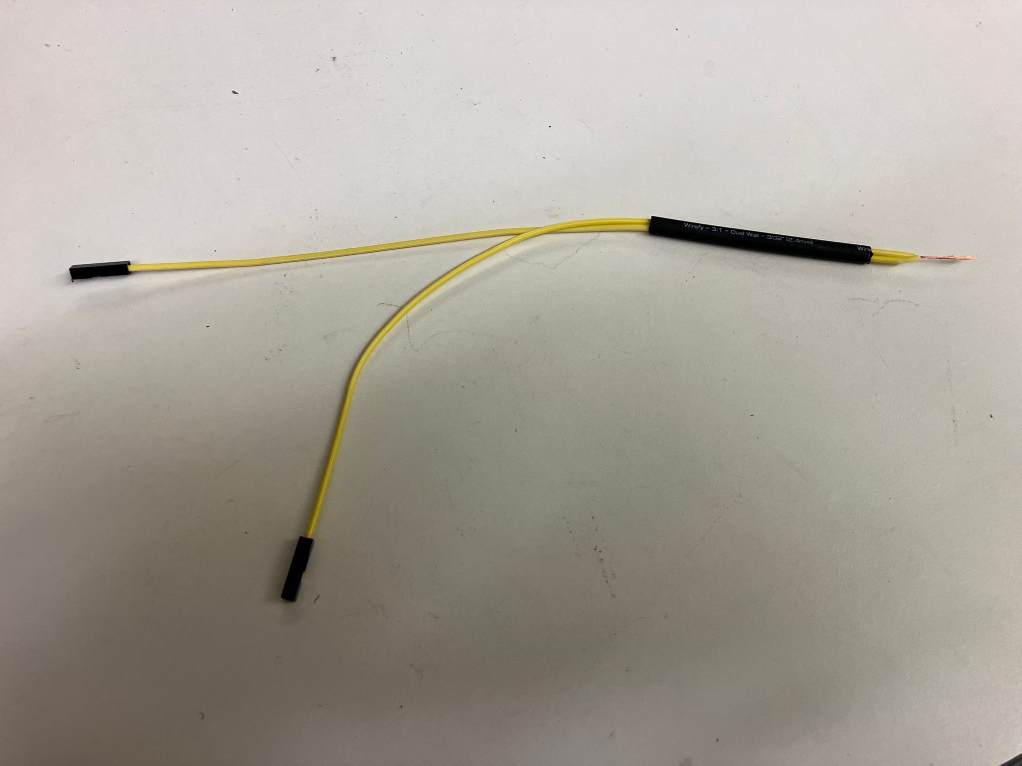
Step-by-step process for creating custom jumper cable assemblies, demonstrating proper wire preparation, soldering techniques, and heat shrink application.
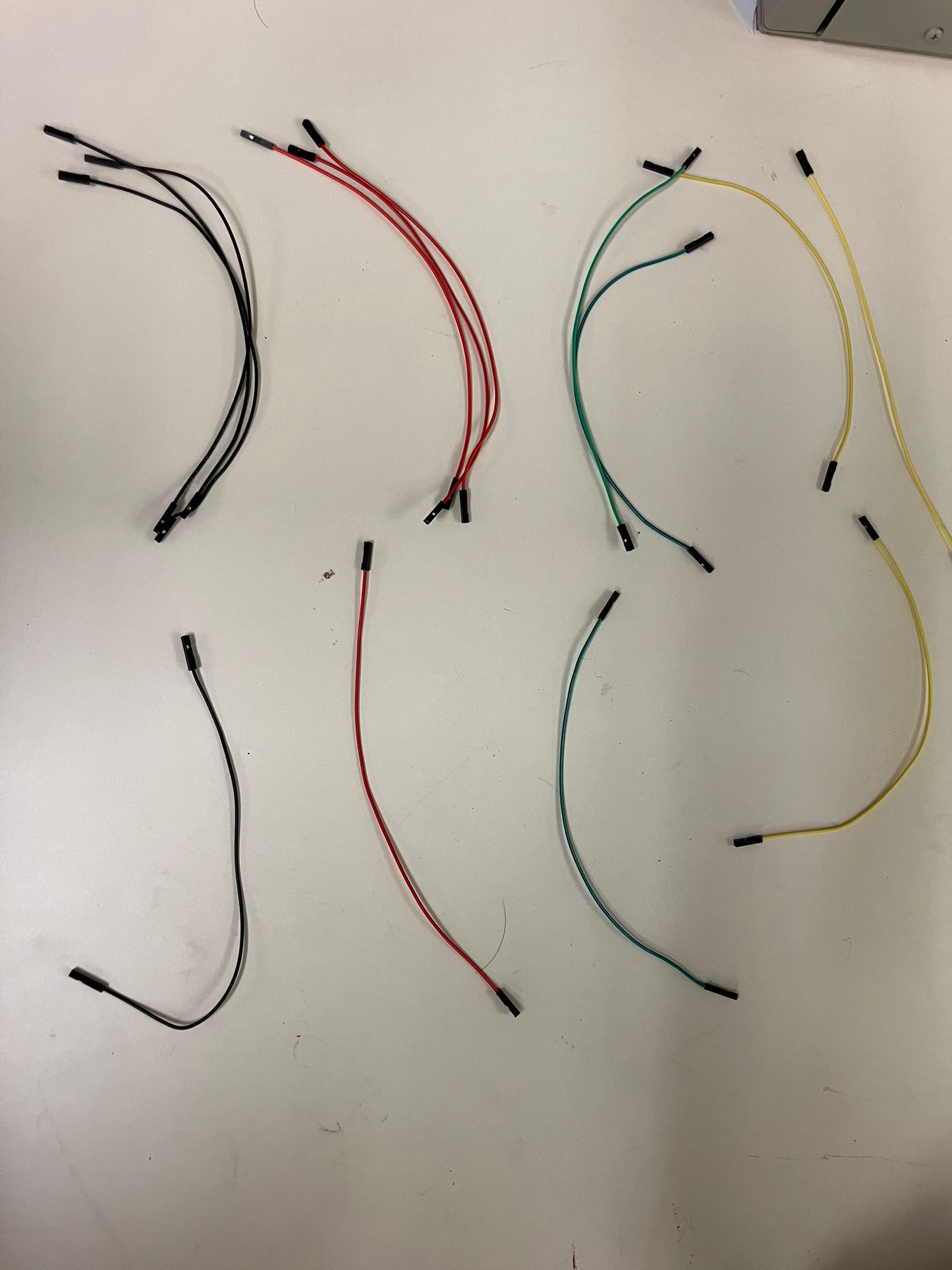
Initial wire preparation showing individual conductors ready for assembly
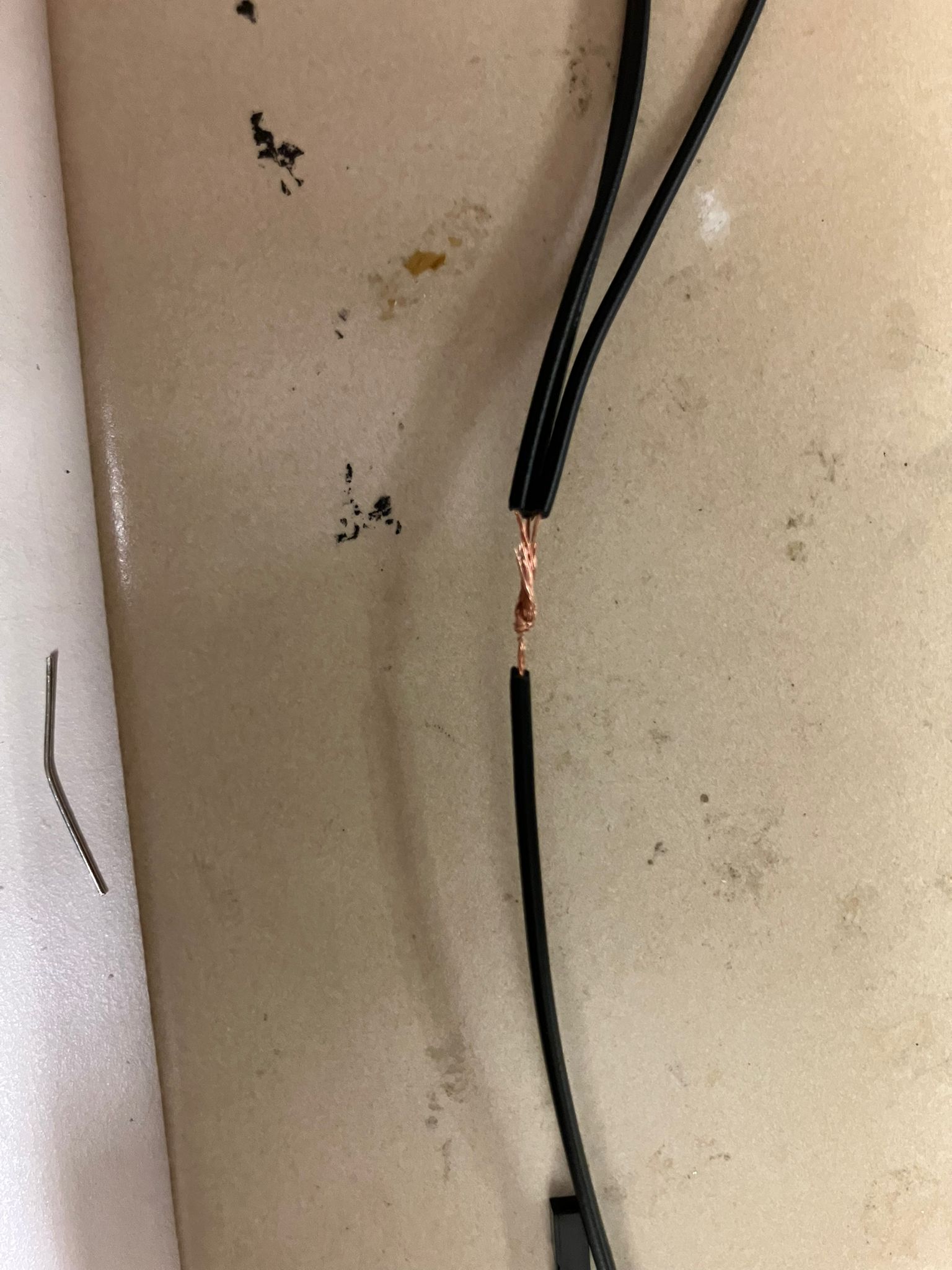
Twisted wire joint preparation before soldering
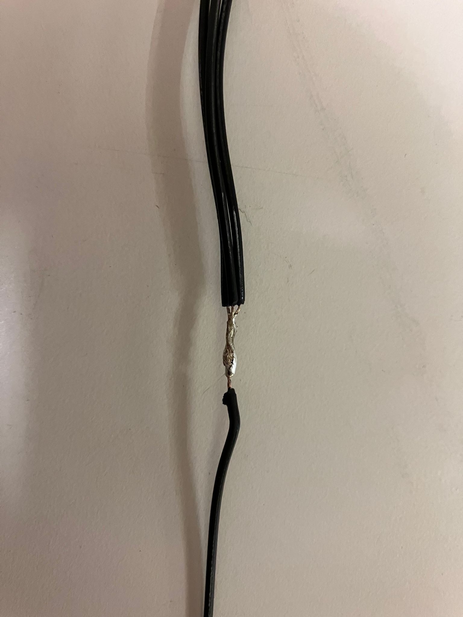
Completed soldered joint showing proper connection and heat distribution
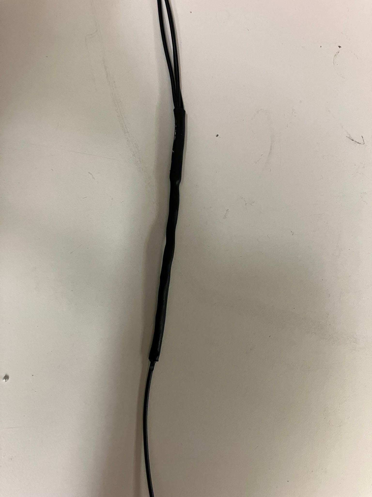
Heat shrink tubing applied for insulation and strain relief
Pro Tip: Heat Shrink Application
Apply heat shrink tubing early in the process to use smaller diameter tubing that's easier to position and provides better insulation coverage.
Demonstration of early heat shrink application for optimal cable assembly
Useful Documentation
Essential resources and detailed guidance for electronics production processes and design rules.
PCB Fabrication Process Details
Source: Anthony Pennes - Slack Message
Detailed guidance on the three available PCB fabrication processes and design rules for successful board production.
Available Fabrication Methods
- Othermill PCB Mill — Preferred method, easiest to get started
- Roland SRM-20 — Runs through MODS interface
- Fiber Laser — Super small traces/spaces, single-sided only, no outlines/holes
Design Rules for Milling
- Trace Width: Keep traces big (>10mil), smaller traces should be kept short
- Spacing: Spaces should be larger than 16mil for reliable production
- Holes: Must be larger than 32mil for the bigger tool (slimmer tool not suitable)
- Vias: Use 0.9mm or 1.5mm holes for copper rivets, avoid holes under components
File Preparation
- Fusion: File → Export → Eagle 9.x compatible .brd file
- KiCad: Fabrication outputs → Gerber files (topcopper, edgecuts, holes, bot copper)
Post-Milling Inspection
Critical: Always perform optical inspection before soldering components. Look for stray copper strands and address them with light sanding, steel scraper, or utility knife.
- Check for copper strands and milling artifacts
- Clean up any issues before component placement
- Much easier to fix problems before soldering
Class Week Resources
Official course resources for electronics production and PCB fabrication.
Lecture Information
-
Electronics Production - MIT Academy
Comprehensive resource covering PCB fabrication methods, milling processes, soldering techniques, and electronics assembly. Includes tutorials on design rules, file preparation, and production workflows.
Recitation Information
-
Electronics Production Recitation - Google Slides
Hands-on tutorial covering PCB fabrication workflows, milling machine operation, soldering techniques, and electronics assembly best practices.
-
Electronics Production Recitation - Vimeo
Video tutorial demonstrating PCB fabrication processes, machine setup, and assembly techniques for electronics production.
Design Files
Complete design files, schematics, PCB layouts, and firmware for the ESP32-S3 development board projects.
ESP32-S3 Development Board Designs
Two complete ESP32-S3 development board designs created using Fusion360 EDA, featuring LED control and button input functionality. View detailed design process and simulation in Week 4.
ESP32-S3 LED Base Design
Standalone LED development board with integrated LED control and button input functionality.
ESP32-S3 LED Connector Design (v6)
Enhanced development board with LED mounted on the back and full pinout connectivity for easy integration with ESP32-S3 development boards.
Arduino Firmware
Button-controlled LED firmware for ESP32-S3 development boards with serial debugging capabilities.
Code Functionality
File Formats & Standards
- PCB Files — Eagle 9.x compatible .brd format for Othermill fabrication
- Firmware — Arduino IDE compatible .ino files for ESP32-S3
- Design Process — Fusion360 EDA workflow with schematic capture and PCB layout
- Simulation — Wokwi online circuit simulation for verification
Reflections & Learnings
Key insights and lessons learned from this week's electronics production work.
Key Points
- Trade-offs between in-house and boardhouse production: speed vs. quality vs. cost considerations
- Design rule checking prevents manufacturing issues—catch errors before fabrication
- Soldering techniques vary by component type—through-hole, SMD, and fine-pitch require different approaches
- Systematic debugging methodology is essential for troubleshooting electronic systems
- Documentation of production process enables reproducibility and knowledge transfer
Production Process Insights
- Understanding the trade-offs between in-house and boardhouse production
- Importance of design rule checking and manufacturability
- Soldering techniques for different component types
- Systematic debugging approach for electronic systems
Contributions
Acknowledgements for help received during this week's electronics production work.
Lab Staff & Instructors
- Anthony — Help fixing traces to 16 mil and making the default traces 16 mil in Fusion360
- Jesse — Walking through the double-sided PCB milling process
- Srikanth — Advice on optimal 760°C solder temperature settings
Classmates & Peers
- Katherine Yan — Peer support during remilling and soldering processes
- Collaborative learning with classmates on design rule characterization, component selection, and troubleshooting techniques
Ethical AI Use
Transparent documentation of AI assistance used in this week's electronics production work.
📋 General Guidelines: See General Commands for Cursor on the homepage for standard guidelines and commands used consistently throughout documentation development.
AI-Assisted Individual Assignment Refinement
This individual assignment section was significantly enhanced by Cursor AI to transform informal challenges and solutions into professional documentation. The AI assisted with creating structured tables for FR1 soldering problems and solutions, organizing project documentation images with proper captions, and updating highlight images with improved visual presentation and linking functionality.
AI-Assisted Week 5 Assignment and Production Updates
This week's individual assignment and production process documentation was significantly enhanced by Cursor AI to transform informal project notes into comprehensive professional documentation. The AI assisted with creating detailed subsections for remilling/soldering processes, front and back LED testing, double-sided milling procedures, rivet installation, and complete design files documentation with proper linking and technical descriptions.
AI-Assisted Content Refinement
Cursor AI helped transform informal training notes into professional SOP documentation, restructure design rule characterization results with improved visual presentation, develop comprehensive individual assignment plans with clear testing protocols, and create structured tables for documenting FR1 soldering challenges and solutions with proper attribution to peer contributors.
 This work is licensed under a
Creative Commons Attribution-NonCommercial-ShareAlike 4.0 International License
This work is licensed under a
Creative Commons Attribution-NonCommercial-ShareAlike 4.0 International License