![[Profile Image Placeholder]](profile.jpg)
Week 4
Electronics Design
Week Highlights
This week focuses on electronics design using EDA tools to create embedded microcontroller systems. We'll learn schematic design, PCB layout, design rule checking, and simulation techniques.
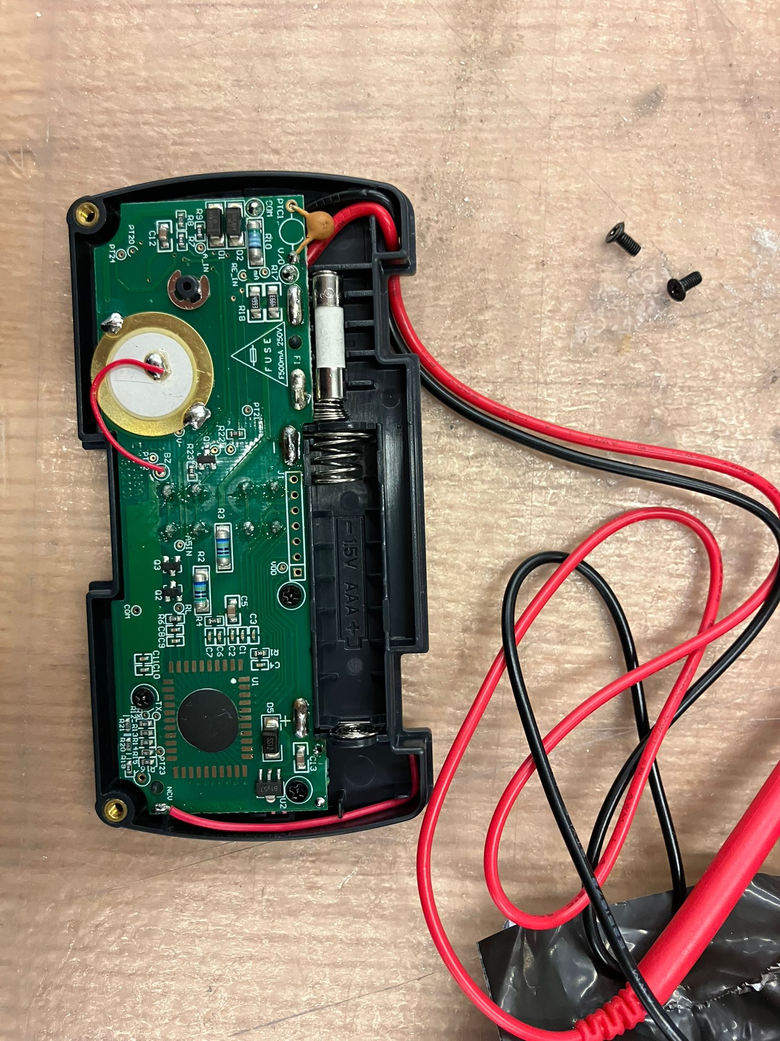
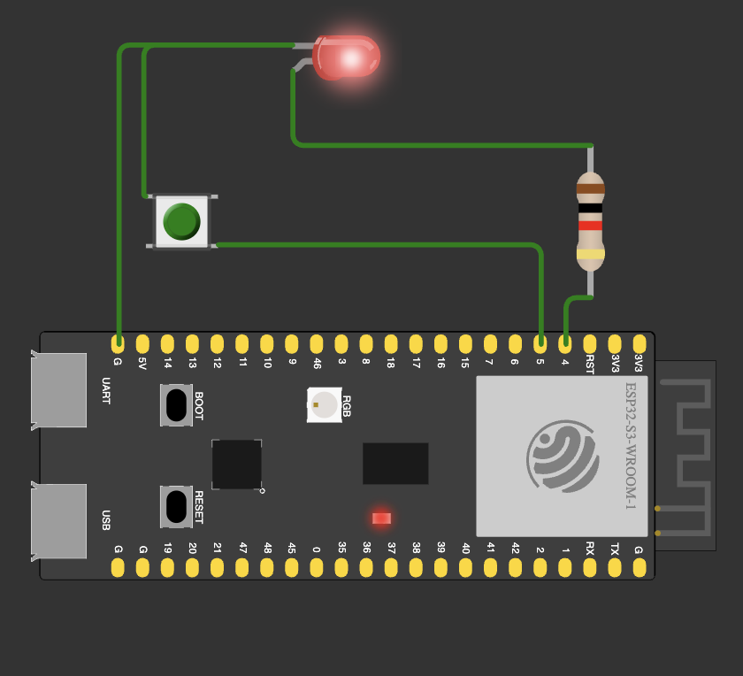
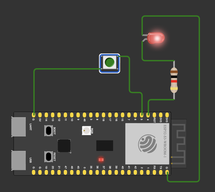
Table of Contents
Course Content
Training & Documentation
Electronics Design Week
This week introduces Electronic Design Automation (EDA) tools for creating embedded microcontroller systems. We'll learn to design schematics, create PCB layouts, perform design rule checks, and simulate circuit operation before fabrication.
This Week's Goals
- Master EDA Tools
Learn KiCad or Eagle for schematic capture and PCB layout design - Design Embedded System
Create a complete microcontroller system using parts from the Fab inventory - Simulate & Verify
Use simulation tools to verify circuit operation before fabrication - Test Equipment Proficiency
Learn to use oscilloscopes, multimeters, and other test equipment
Assignments
- Group Assignment
Use test equipment to observe embedded microcontroller operation - Individual Assignment
Design embedded system with EDA tool, check design rules, and simulate
Tools & Materials
- EDA Software
KiCad, Eagle, or Altium Designer - Test Equipment
Oscilloscope, multimeter, function generator - Simulation Tools
LTspice, ngspice, Wokwi - Fab Inventory Parts
Microcontrollers, passive components, connectors
Training Documentation
Essential training materials for electronics design, EDA tools, and test equipment operation.
EDA Tool Training
- KiCad schematic capture
- PCB layout and routing
- Design rule checking
- Footprint libraries
Test Equipment
- Oscilloscope operation
- Multimeter measurements
- Function generator setup
- Probe calibration
Useful Documentation
Essential resources for electronics design, EDA tools, and embedded systems development.
EDA Tools & Software
- KiCad — Open-source EDA suite
- Eagle — Professional PCB design
- Altium Designer — Advanced PCB design
- Wokwi — Online Arduino simulator
Simulation & Testing
- LTspice — Circuit simulation
- ngspice — Open-source SPICE
- Falstad Circuit — Interactive simulation
- Fab Inventory — Available components
Test Equipment Guides
- Oscilloscope Basics — Tektronix tutorial
- Multimeter Usage — SparkFun guide
- MIT Academy Electronics Design — Course reference
Design Guidelines & EDA Tools
Key design rules and EDA tool recommendations from course Slack discussions.
PCB Design Rules
- 1 mil = 0.001 inches (not millimeters!)
- Trace width: >10mil minimum
- Trace spacing: >16mil between traces
- Component sizes: ~1206 or larger recommended
- Flexibility: Break out extra pins, multiple power/ground copies
Microcontroller Options
- Xiao: All-in-one, multiple footprint choices
- ATtiny/SAMD: More parts but powerful and cheap
- Note: Tape-bottomed components need Kapton tape
EDA Tool Options
Leo's Open Source Tool
Easiest starting point for this class
KiCad
Open source, widely used, improved UI
Fusion 360
Cloud-synced part libraries, team access
Feedback Available: Send schematic/PCB files and screenshots for design review. View Design Guidelines Discussion • View EDA Tools Discussion
Class Week Resources
Official course resources for electronics design and EDA tools.
Lecture Information
-
Electronics Design - MIT Academy
Comprehensive resource covering electronics design principles, EDA tools, circuit simulation, PCB design, and embedded systems development. Includes tutorials on KiCad, Eagle, and other EDA platforms.
Recitation Information
-
Electronics Design Recitation - Vimeo
Hands-on tutorial covering electronics design workflows, EDA tool usage, circuit simulation techniques, and PCB design best practices for embedded systems development.
Group Assignment: Test Equipment Operation
Use the test equipment in your lab to observe the operation of an embedded microcontroller. This assignment focuses on understanding how to use oscilloscopes, multimeters, and other test equipment to analyze microcontroller behavior and circuit operation.
Group Assignment Link: View Complete Group Assignment Summary
Test Equipment Available
The following test equipment was utilized to observe and analyze microcontroller operation. Multimeter and oscilloscope provide 99% of the information needed for comprehensive analysis.
Multimeter
Essential for basic measurements - voltages (slow, twice a second), resistances, and current (in series)
Oscilloscope
High-speed analysis - voltages (fast, 5 million times a second) and digital signal decoding
Logic Analyzer
Digital signal analysis - both cheap and professional models available, can also be done on oscilloscope
Function Generator
Signal generation for testing receiving ends of boards - most scopes have built-in generators
Power Supply
Controlled power delivery for stable microcontroller operation
Breadboard
Circuit prototyping and testing platform
Test Equipment Procedures & Observations
Detailed procedures and observations using various test equipment to analyze microcontroller operation:
Multimeter Measurements
- Voltage Measurements: Slow sampling rate (twice per second) for steady-state analysis
- Resistance Testing: Component and trace resistance verification
- Current Measurement: Series connection required for accurate current readings
- Continuity Testing: Resistance mode then 'select' for continuity (beeps under 50 ohms)
Oscilloscope Analysis
- High-Speed Sampling: 5 million times per second for detailed signal analysis
- Probing Technique: Ground alligator clip to ground, main probe to signal pins
- 5V Supply Analysis: Measured 4.96V actual with ~300mV noise/ripple
- 3.3V Supply Analysis: Measured 3.23V actual with similar ~300mV ripple
Serial Communication Analysis
Digital signal decoding and serial communication protocol analysis using oscilloscope capabilities.
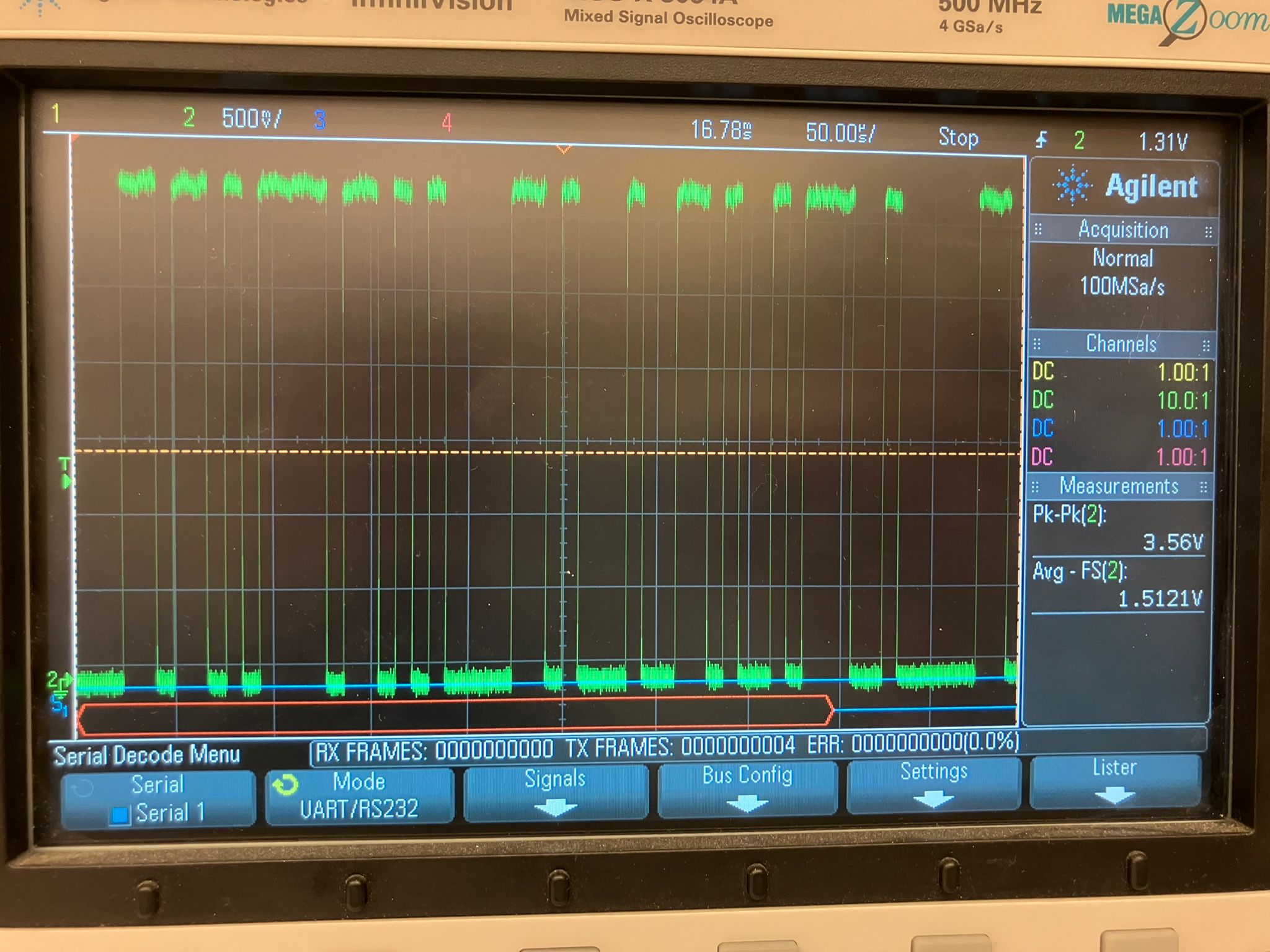
Serial Signal Analysis: Oscilloscope capture showing digital serial communication signals with clear 1s and 0s pattern, enabling ASCII character decoding and protocol verification.
I2C Communication Analysis
- SCL Clock Line: 400 kHz square wave observed (falling edge trigger)
- SDA Data Line: Serial data stream of 1s and 0s
- Protocol Verification: Proper start/stop conditions and addressing observed
ECG Signal Testing
- Low-Pass Filter Setup: Configure oscilloscope with low-pass filter
- Probe Placement: Shoulder-to-shoulder probe positioning
- Signal Observation: Clear electrocardiogram waveform captured
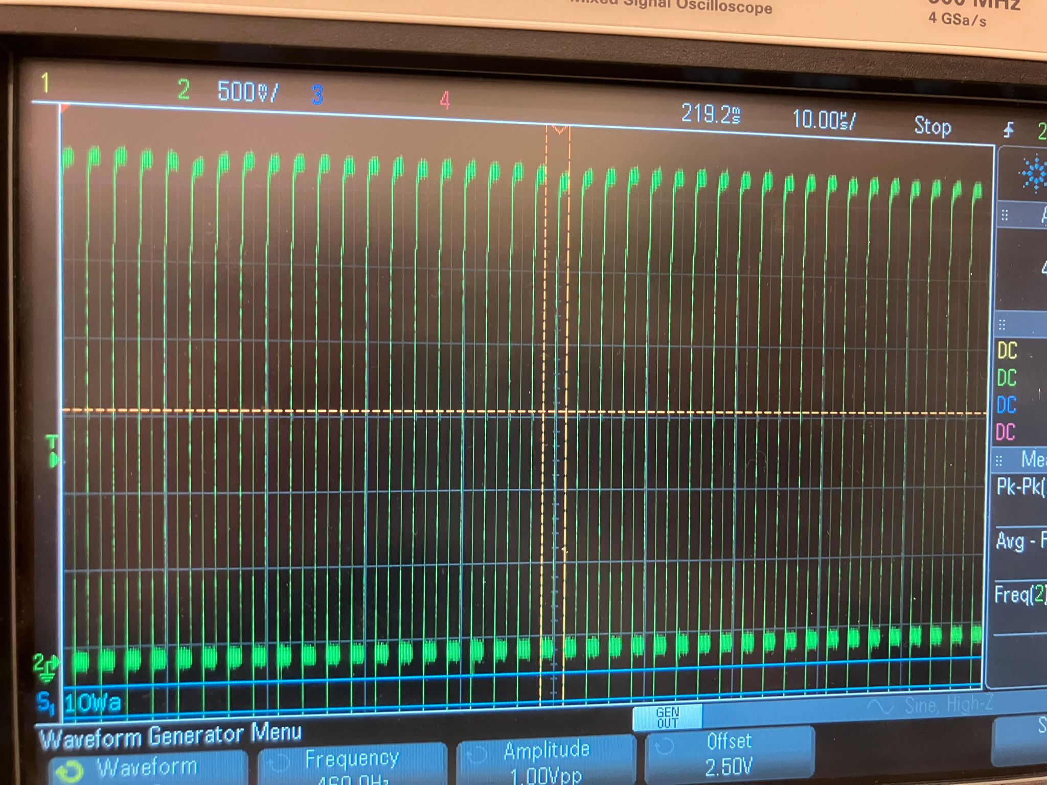
SCL Clock Signal: I2C SCL line showing clean 400kHz square wave
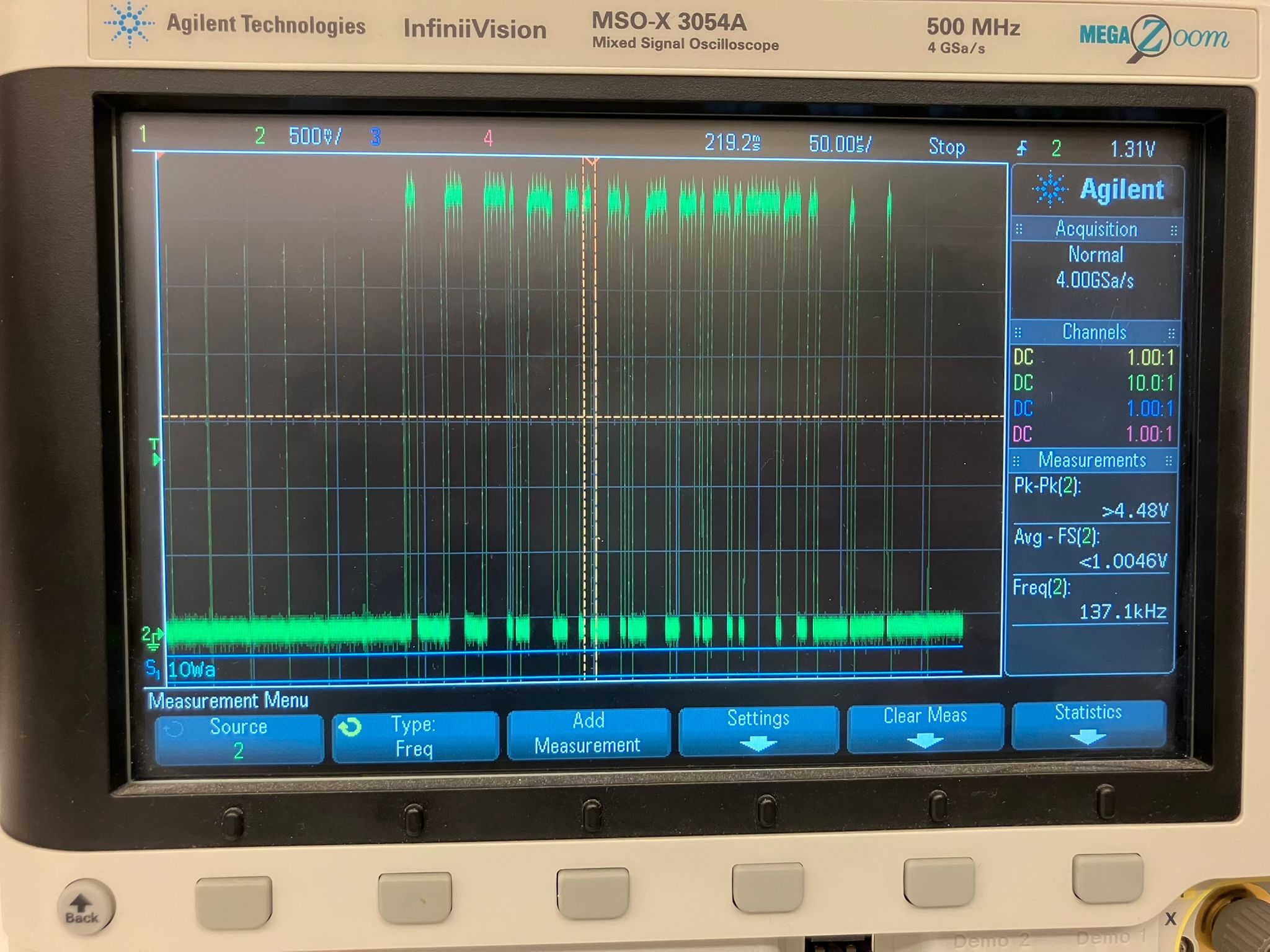
SDA Data Signal: I2C SDA line showing data bits changing on SCL falling edges
Key Findings & Practical Applications
Comprehensive analysis of test equipment effectiveness and real-world applications:
Power Supply Analysis
- 5V Rail: Measured 4.96V with ~300mV noise/ripple
- 3.3V Rail: Measured 3.23V with similar ripple characteristics
- Application: Understanding noise characteristics for stable operation
Equipment Effectiveness
- Multimeter: Essential tool providing 99% of needed information
- Oscilloscope: High-speed sampling (5MHz) for detailed analysis
- Integration: Most oscilloscopes include built-in signal generators
Test Equipment Setup Procedures
Oscilloscope Probing Setup:
- Plug alligator clip of ground probe to ground reference
- Use main probe clip to probe signal pins
- Adjust oscilloscope view for optimal signal display
- Start with 5V supply pin for initial voltage verification
Multimeter Continuity Testing:
- Set multimeter to resistance mode
- Press 'select' function for continuity mode
- Device beeps when resistance is under 50 ohms
- Press function twice for portable multimeter operation
Key Learnings
Understanding how to properly probe circuits, interpret oscilloscope traces, and use test equipment to diagnose embedded system operation. This foundation is essential for debugging and verifying circuit designs before and after fabrication. The systematic approach starting with basic power supply verification and progressing to complex signal analysis ensures comprehensive coverage of all critical operational aspects.
Individual Assignment: EDA Design & Simulation
Use an EDA tool to design an embedded microcontroller system using parts from the inventory, check its design rules for fabrication, and simulate its operation. This assignment involves complete schematic capture, PCB layout, design rule checking, and circuit simulation.
Fusion360 Design Process
Complete step-by-step workflow for designing embedded systems in Fusion360 EDA:
Schematic Design Steps
-
1
Add board outline and define board dimensions
-
2
Add switch component and configure properties
-
3
Add LED component with proper orientation
-
4
Add resistor for current limiting
-
5
Add net connectors for dev board integration
PCB Layout Steps
-
6
Switch to PCB view and arrange components
-
7
Ensure no component overlaps
-
8
Route traces (flip and add holes if needed)
-
9
Resize board and create polygon pour
-
10
Add mounting holes and finalize design
Simulation: After completing the PCB design, remake the circuit in simulation websites like Wokwi to verify operation before fabrication.
Board Designs
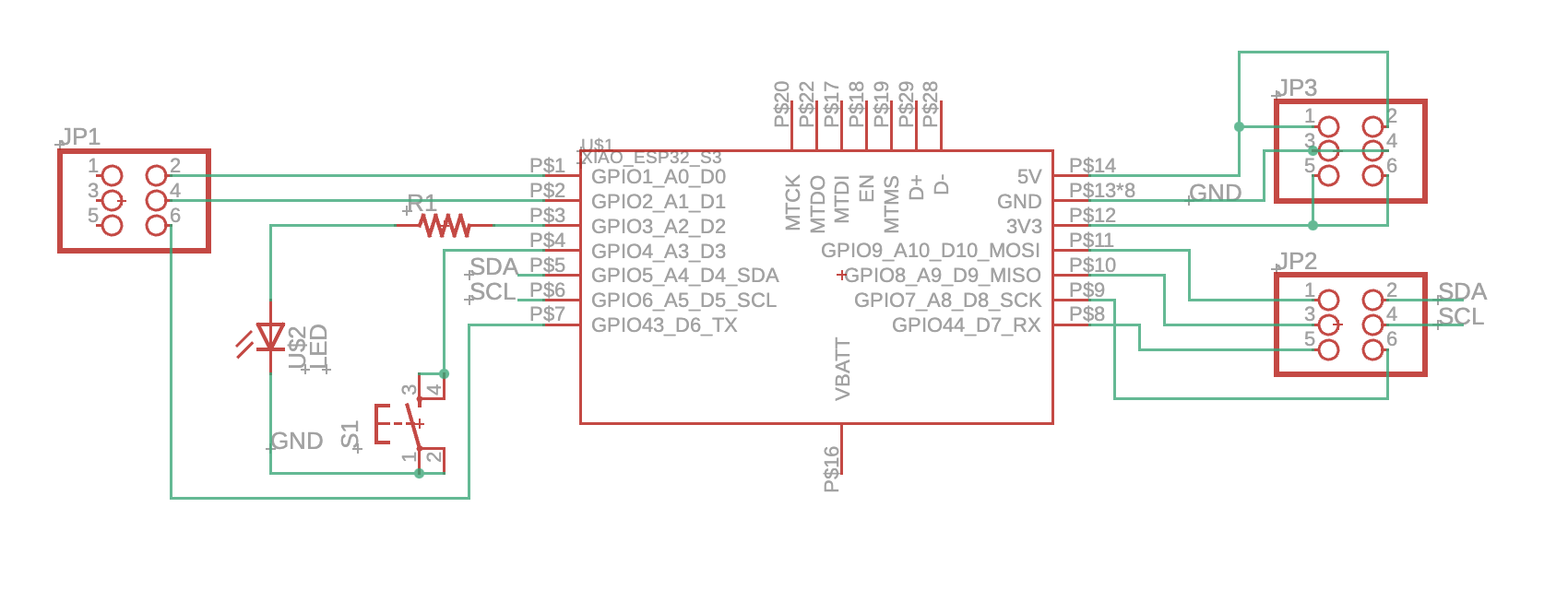
Two ESP32S3-based designs created using Fusion360 EDA: a standalone LED board and a dev board connector with LED on the back.
ESP32S3 LED Base Design
Standalone LED board design for ESP32S3 microcontroller with integrated LED and supporting circuitry.
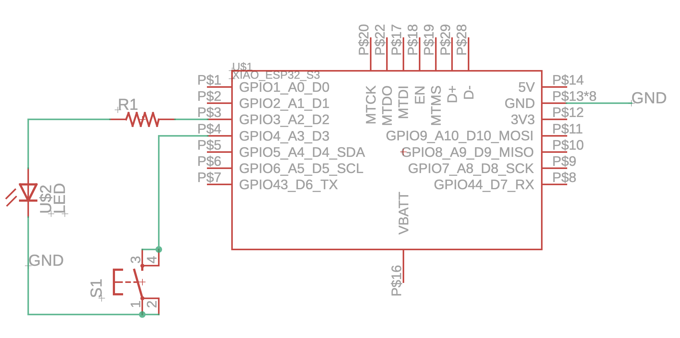
Schematic Design
📥 Download .sch file
PCB Layout with Polygon Pour
📥 Download .brd fileESP32S3 Dev Board Connector Design
Development board connector design with LED mounted on the back for easy integration with ESP32S3 development boards.
Schematic Design
📥 Download .sch file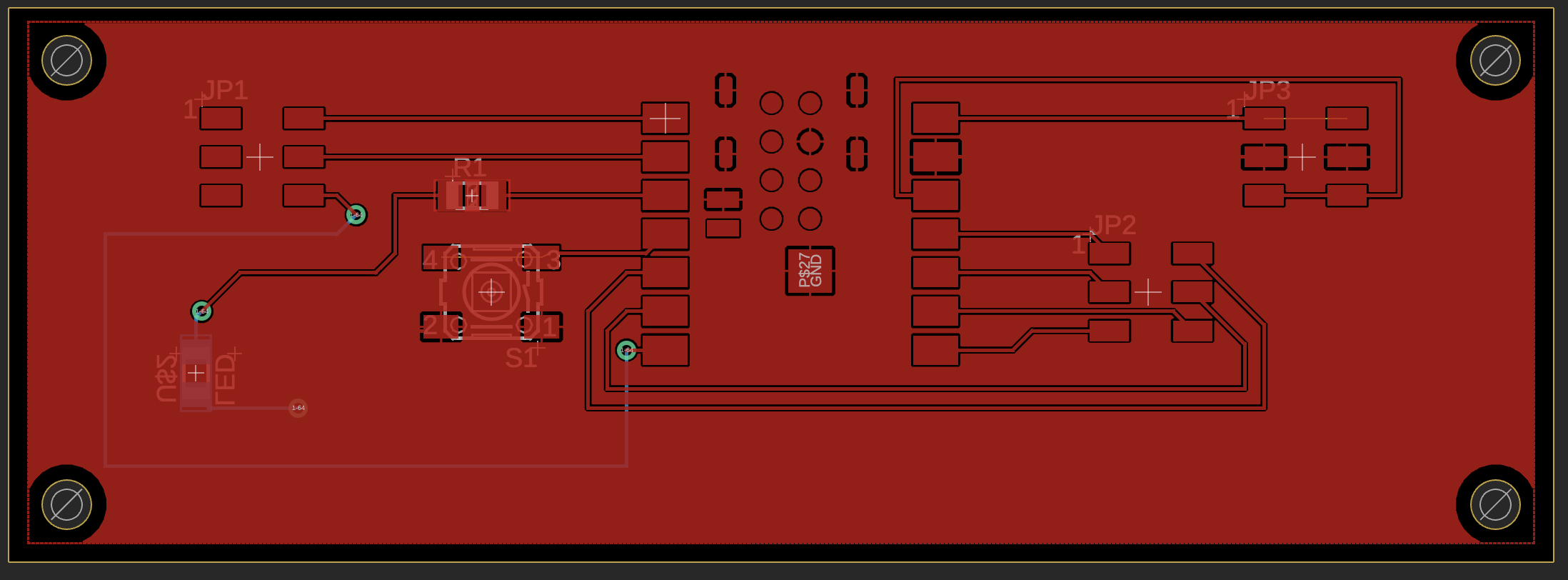
PCB Layout with Polygon Pour
📥 Download .brd fileDesign Process
- Schematic capture
- Component selection
- PCB layout design
- Design rule checking
Simulation & Verification
- Circuit simulation
- Timing analysis
- Power consumption
- Signal integrity
Design Requirements
- Use components from Fab inventory
- Include microcontroller and supporting circuitry
- Pass design rule checks for fabrication
- Simulate operation before fabrication
Circuit Simulation & Verification
Interactive circuit simulations created using Wokwi to verify the ESP32S3 LED circuit designs before fabrication. These simulations demonstrate the button-controlled LED functionality and help validate the circuit operation.
ESP32S3 LED Circuit Simulation 1
Primary simulation showing button-controlled LED circuit with ESP32S3 microcontroller.
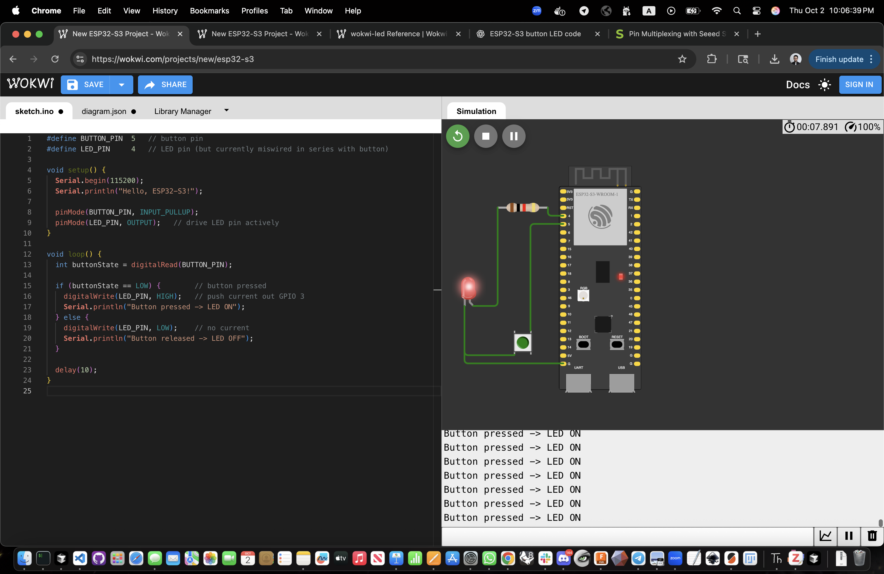
Interactive Simulation: Button-controlled LED circuit with ESP32S3
Simulation Links
Code Files
ESP32S3 LED Circuit Simulation 2
Alternative simulation configuration with the same circuit functionality.
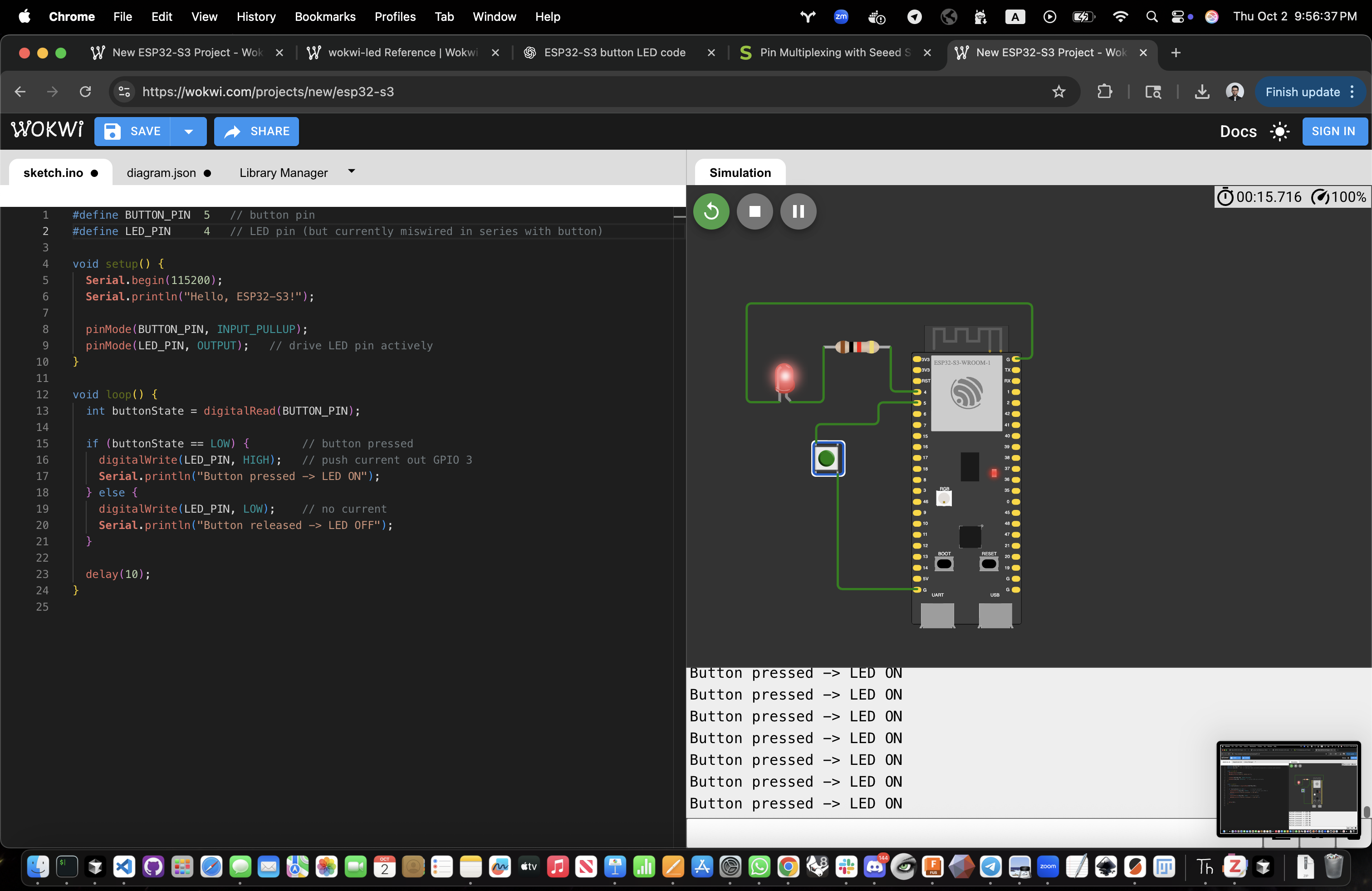
Alternative Configuration: Same circuit with different simulation setup
Simulation Links
Code Files
Arduino Code Explanation
The same Arduino code is used for both simulations, implementing a simple button-controlled LED circuit.
#define BUTTON_PIN  5   // button pin
#define LED_PIN     4   // LED pin (but currently miswired in series with button)

void setup() {
  Serial.begin(115200);
  Serial.println("Hello, ESP32-S3!");

  pinMode(BUTTON_PIN, INPUT_PULLUP);
  pinMode(LED_PIN, OUTPUT);   // drive LED pin actively
}

void loop() {
  int buttonState = digitalRead(BUTTON_PIN);

  if (buttonState == LOW) {        // button pressed
    digitalWrite(LED_PIN, HIGH);   // push current out GPIO 3
    Serial.println("Button pressed -> LED ON");
  } else {
    digitalWrite(LED_PIN, LOW);    // no current
    Serial.println("Button released -> LED OFF");
  }

  delay(10);
}
Code Functionality
- Button Input: GPIO 5 with internal pullup resistor
- LED Output: GPIO 4 drives LED directly
- Serial Monitor: Debug output at 115200 baud
- State Detection: LOW = pressed, HIGH = released
Circuit Behavior
- Press Button: LED turns ON, serial message
- Release Button: LED turns OFF, serial message
- Real-time: 10ms loop delay for responsiveness
- Debugging: Serial output for troubleshooting
EDA Tools & Workflow
Overview of Electronic Design Automation tools and the complete design workflow from schematic to fabrication.
Schematic Design
- Component library management
- Symbol creation and editing
- Netlist generation
- Electrical rule checking
PCB Layout
- Component placement
- Routing and trace optimization
- Design rule checking (DRC)
- Gerber file generation
Recommended EDA Tools
KiCad
Open-source, full-featured EDA suite with excellent community support
Eagle
Professional PCB design tool with extensive component libraries
Altium
Advanced PCB design with integrated simulation capabilities
Design Files
All design files, schematics, PCB layouts, and simulation files for the electronics design assignments.
Schematic Files
- schematic.kicad_sch — KiCad schematic
- schematic.pdf — PDF schematic
- bom.csv — Bill of materials
PCB & Simulation
- pcb.kicad_pcb — KiCad PCB layout
- gerber.zip — Gerber files for fabrication
- simulation.asc — LTspice simulation
Reflections & Learnings
Key insights and learnings from the electronics design week, including challenges faced and skills developed.
Key Points
- EDA tool workflow mastery is essential—understanding schematic capture, PCB layout, and design rule checking
- Simulation before fabrication saves time and materials—verify designs before committing to board production
- Component selection requires balancing functionality, availability, and cost constraints
- PCB layout best practices (signal integrity, power distribution) directly impact board performance
- Understanding fabrication constraints (minimum trace width, via size) is critical for manufacturable designs
Technical Learnings
- EDA tool workflow mastery
- Design rule checking importance
- Simulation before fabrication
- Test equipment proficiency
Design Insights
- Component selection strategies
- PCB layout best practices
- Signal integrity considerations
- Fabrication constraints
Contributions
Acknowledgements and team contributions for the electronics design week assignments.
Group Assignment
- Collaborative test equipment setup
- Shared measurement techniques
- Documentation of procedures
Individual Work
- Complete EDA design workflow
- Simulation and verification
- Design file documentation
Ethical AI Use
AI tools used to assist with electronics design, EDA tool learning, and circuit simulation guidance.
📋 General Guidelines: See General Commands for Cursor on the homepage for standard guidelines and commands used consistently throughout documentation development.
AI-Assisted Tasks
- EDA tool workflow guidance and troubleshooting
- Circuit simulation setup and parameter optimization
- Design rule checking interpretation and fixes
- Component selection and datasheet analysis
Week 4 HTML Template Creation
Cursor AI assistance for creating the week4.html template with comprehensive electronics design content, including EDA tools, assignments, and documentation resources.
Focus: HTML template creation, electronics design content population, assignment structure, and documentation integration
Individual Assignment Enhancement
Cursor AI assistance for updating the individual assignment section with detailed Fusion360 design process, board design images, and improved visual presentation.
Focus: Fusion360 design process documentation, board design image integration, visual alignment improvements, and highlights section updates
Week 4 Group Assignment Update
Cursor AI assistance for updating the Week 4 group assignment section with comprehensive test equipment details, image link updates, and group page integration.
Focus: Group assignment content integration, test equipment documentation, image path updates, and group page link addition
 This work is licensed under a
Creative Commons Attribution-NonCommercial-ShareAlike 4.0 International License
This work is licensed under a
Creative Commons Attribution-NonCommercial-ShareAlike 4.0 International License