Transmission lines
Microstrips and coplanar waveguides
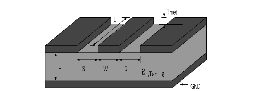
A microstrip transmission line consists of a signal trace, and a return ground plane, with a dielectric in between:

The impedance $Z_0$ and effective permittivity $\epsilon_{\rm eff}$ can be found from the following model:
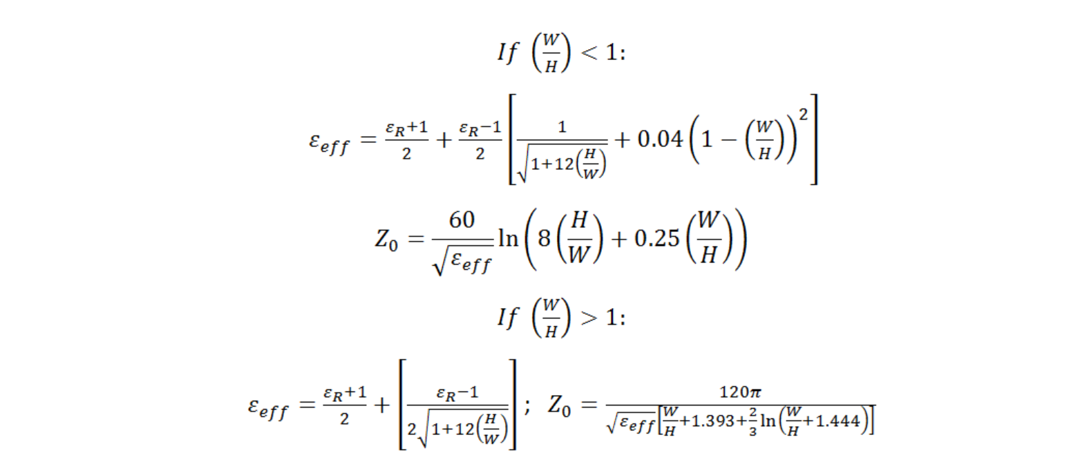
(from https://www.pasternack.com/t-calculator-microstrip.aspx)
To reach a low impedance, microstrip requires either thick traces, a thin dielectric, or a high permittivity substrate. Since I plan to use FR1 substrate of fixed thickness 1.6mm and relatively low permittivity, this type of transmssion line will not be practical.
An improvement over microstrips is coplanar waveguide lines. They have additional ground lines left and right of the strip, significantly lowering the overall impedance:
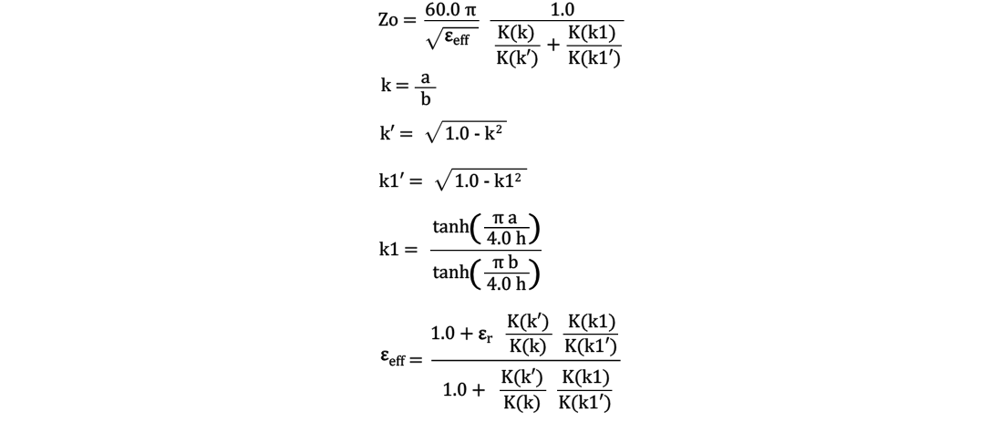
The impedance derivation is much more involved. Here is a model, with $a$ being the trace width $w$, and $b=w+2g$, in which $g$ is the gap:
Implementation
Using the formula above, I designed a strip targeting an impedance of $Z_0=50~\Omega$, to match the cables and equipment I already have. The permittivity of the FR1 substrate I’m using is unknown. Let’s use $\epsilon_r = 4$ for now, providing the following parameters for a board thickness of 1.6 mm:
- Trace width: 2 mm
- Trace gap: 0.4 mm
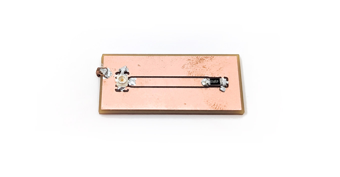
Here is the fabricated line, with a $Z_0=50~\Omega$ load and a copper braid connecting the top and bottom ground planes:
When I checked the reflection S11 with a VNA, I was disappointed. The reflection was pretty high, a full -15 dB at 2.4 GHz. However, swapping the load resistor for a $62~\Omega$ one provided a much smaller reflection:
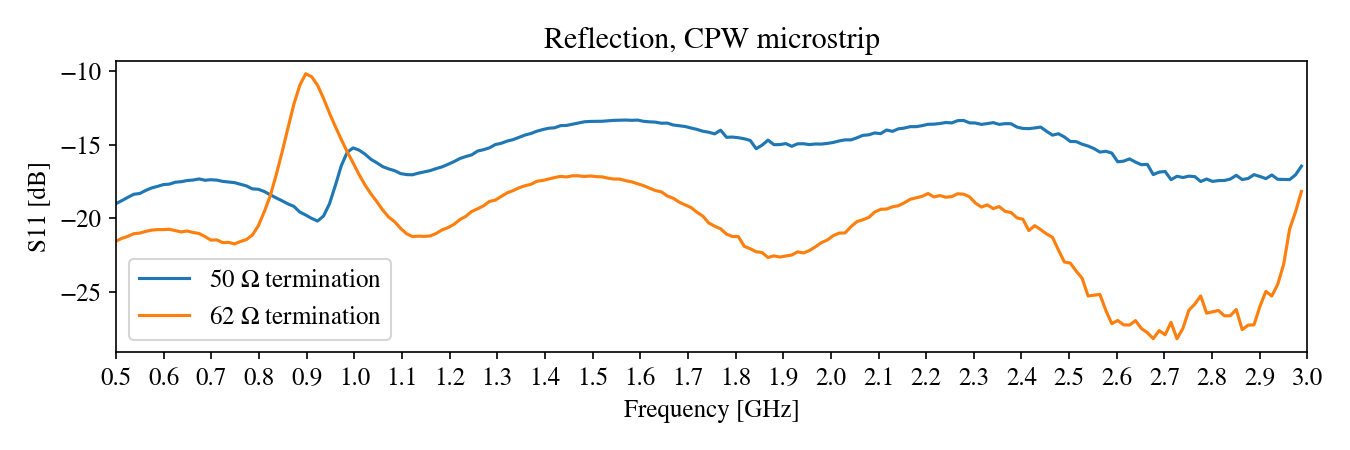
This result suggests that the $\epsilon_r$ of this FR1 board differs from the assumed value of 4. using the model above, I found that $\epsilon_r=2.5$ more closely matched the observations. To confirm this, I made a new line with a width of 3.1 mm instead:

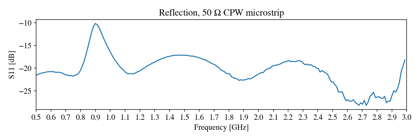
As planned, this new design is well matched to the $50~\Omega$ load:
Impedance matching
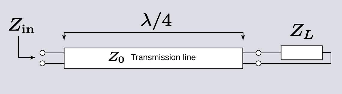
Quarter-wave impedance transformer
Quarter-wave impedance transformer are narrowband devices capable of completely matching two devices of different impedances. Their impedance and transmission delay is carefully chosen to seamlessly transmit the maximal amount of power to the load at the frequency of interest.
 (from https://en.wikipedia.org/wiki/Quarter-wave_impedance_transformer)
For a transmission line of impedance $Z_0$ of length $l$ connected to a load $Z_L$, the perceived input impedance $Z_{\rm in}$ is found to be (neglecting losses):
\[Z_{\rm in} = Z_0 \frac{Z_L + i Z_0 \tan(kl)}{Z_0 + i Z_L \tan(kl)}\]where $k=\frac{2\pi}{\lambda}$ is the wavenumber in the transmission medium. If $l = \lambda / 4$, the tangent terms diverge and the limit can be found as:
\[Z_{\rm in} \approx Z_0 \frac{i Z_0 \tan(kl)}{i Z_L \tan(kl)} = \frac{Z_0^2}{Z_L}\]Showing that the impedance of the line must be the geometric mean between $Z_{\rm in}$ and $Z_{\rm L}$:
\[Z_0 = \sqrt{Z_{\rm in} Z_{\rm L}}\]Let’s build a short transmission line matching the input cable’s impedance of $50~\Omega$ and load of $75~\Omega$. The transformer’s impedance must be $61.24~\Omega$, and its length is a function of the frequency of interest. Since I plan to design an antenna transmitting WiFi signals are $f = 2.44~{\rm GHz}$, let’s pick that frequency.
Using the CPW microstrip model from above and assuming a relative permittivity $\epsilon_r = 2.5$, we find that the width of the transformer’s track should be 1.95 mm wide. The length of the transformer $l=\lambda / 4$ is a function of the permittivity of the medium. After a few trials, I found that using $\epsilon_r = 2.5$ when estimating the wavenumber did not lead to good results. Looking back at the equations for coplanar waveguides, an effective permittivity $\epsilon_{\rm eff}$ is provided, which should be more accurate than $\epsilon_r$. I estimated it as 1.75, giving a quarter-wave length of $l=23.5$ mm.
Here is the transformer after machining and soldering, with a resistive load of $75~\Omega$:
![]()
I then measured the reflection loss S11 using a VNA. I was expecting a clear dip around $f = 2.44~{\rm GHz}$, but instead saw one dip at a lower frequency, and another one at a higher one:
![]()
Either way, the reflection loss is low: -20 dB around the frequencies of interset. After finding a more accurate estimate of $\epsilon_{\rm eff}$, I decided to change the length to 22.65 mm. Rather than make another terminated line, I made a two-port device that transforms the signal to $75~\Omega$, and back to $50~\Omega$:
![]()
This let me measure the transmission S21 using the VNA:
![]()
The reflection and transmission taken together tell a more complete story: a slight increase in transmission can be seen around $f = 2.5~{\rm GHz}$. Either way, those are very small difference and the transmission is already high across the board. I suspect this line is too short to see any significant effect.
![]()
Klopfenstein taper
The quarter-wave impedance transformer is a narrowband device, not designed for broadband operation. The Klopfenstein taper addresses this by progressively changing the impedance over a long distance. Intuitively, higher frequencies (shorter wavelengths) will be less affected by the taper. This lets Klopfenstein taper devices operate at a wide range of frequencies.
Klopfenstein tapers have two main parameters: the desired reflection loss S11, and the starting frequency at which this loss is achieved.
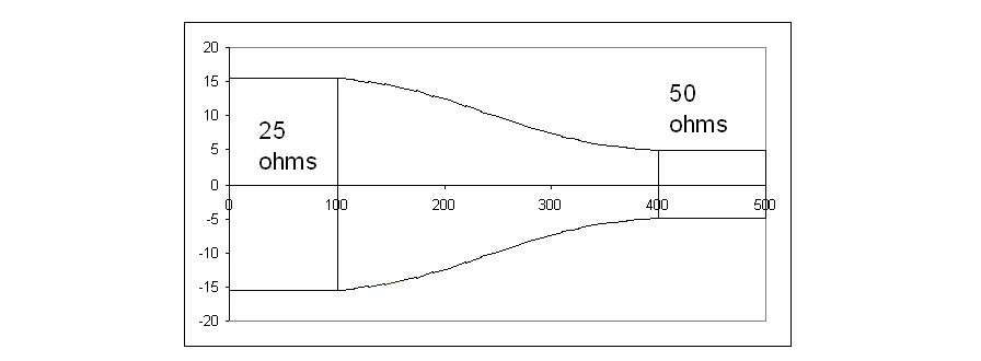
Here is an example of a taper; note that the horizontal axis is not to scale:
In practice, Klopfenstein tapers seem to be very long. I found a Python tool that computes the impedance profile given the desired constraints: https://github.com/andrew-burger/KlopfensteinTaper
The tool outputs an impedance profile, which can be mapped to geometric parameters using the transmission line models from above. Here is a Klopfenstein taper I designed using this tool:
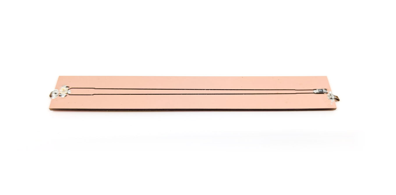
This was designed to obtain a -20 dB reflection loss above 2 GHz. Here is the result of testing it with a VNA:
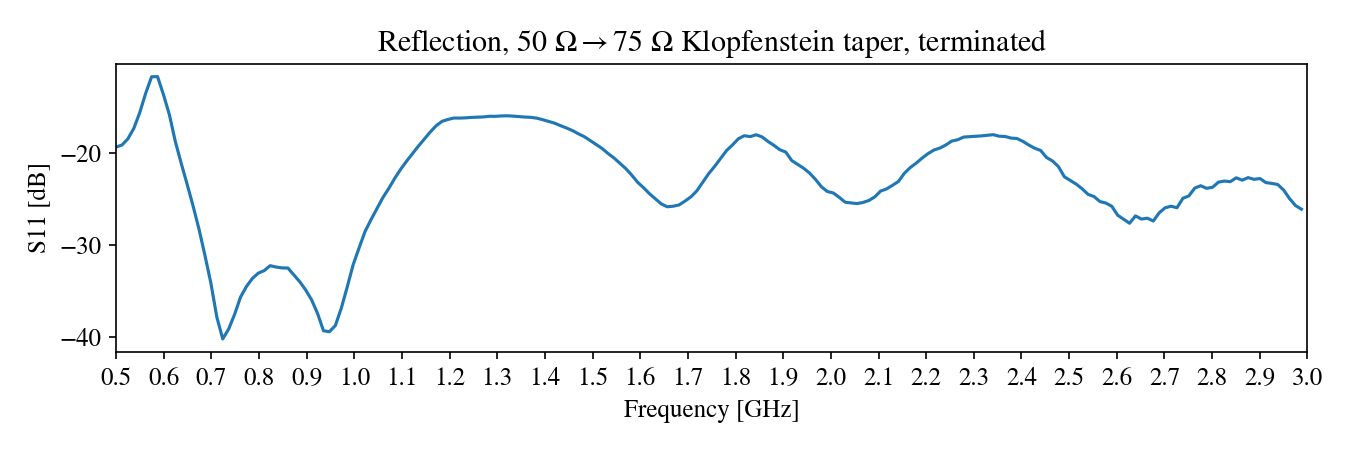
While this reflection still seems high, it outperforms the quarter-wave transformer in higher frequencies:
![]()