Week 5: Custom PCB for Hello Board
assignment: redraw the echo hello-world board, add (at least) a button and LED (with current-limiting resistor), check the design rules, and make it
what I made: custom PCB with green LED and pushbutton
Designing the PCB
For this week's project, we return to the land of electronics and tiny surface-mount components. After spending the day in class learning about the various electronic components and how they work (more or less), it was our task to replicate the "hello" board example using an electronic CAD software like Eagle so that we could print the board and solder components on to it. In addition to the base design that was provided, we had to add an additional button and LED to give the board new functionality.
I've worked with Eagle some before in the past, but with only having access to one layer for this project (such is the nature of milling our own boards instead of creating custom PCBs with multiple layers) I was looking forward to the challenge of routing wires on this setup. I ran into some trouble right off the bat when I began placing schematic components from the fab library in Eagle and noticed that Eagle wasn't letting me move said components. I spent 45 minutes going through troubleshooting forums online - it turns out the problem was a combination of an older version of Eagle (I was running 7.6.0 when the newest version was 7.7.0) and the fact that the fab library I had downloaded had somehow been corrupted. After grappling with the software for a while, Eagle finally let me place components.
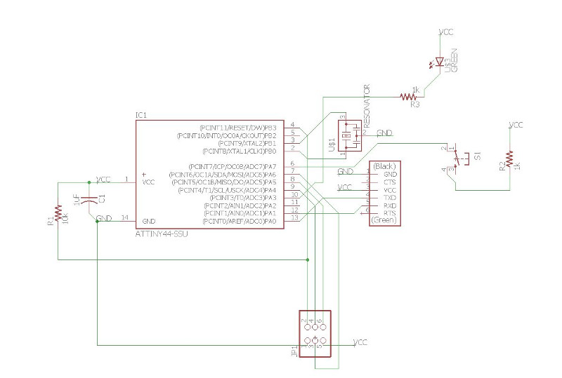
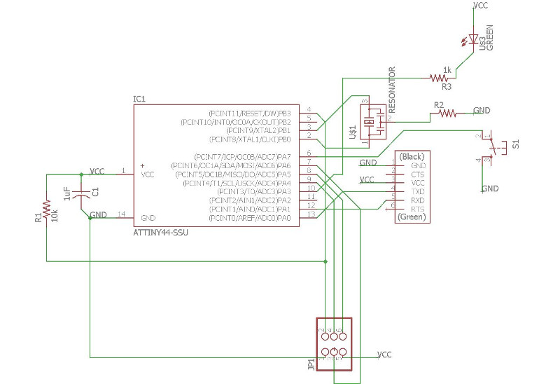
Setting up the schematic was relatively easy - Eagle is generous about connecting components because when you name two wires the same name, they become electrically connected even if no connecting wire is shown in the diagram. This allowed me to produce a very clean schematic without too much insane overlap of connecting wires (as would usually be the case if this were a schematic drawn by hand).
The most difficult part of the whole process was understanding the I/O setup of the Attiny44. As an electrical engineer, I feel it's my obligation to dig a little deeper into the Attiny44 design and architecture to truly understand what is going on at a lower level. After going down a rabbit hole of UART, SPI and I2C for a couple hours, I decided to move on to constructing the board layout.
The finished schematic is nearly identical to the example board except I have now included an active-low pushbutton tied to PA7 (pin 6) that utilizes the internal 10k pull-up resistor of that processor pin. I have also included a green LED on PA3 (pin 10) with a 1k current-limiting resistor. The signal is once again active low because the processor is much better at sinking current then it is at sourcing current. Pins PA7 and PA3 were chosen for these additional components because the geography of traces on the board means these two pins are actually the most accessible.
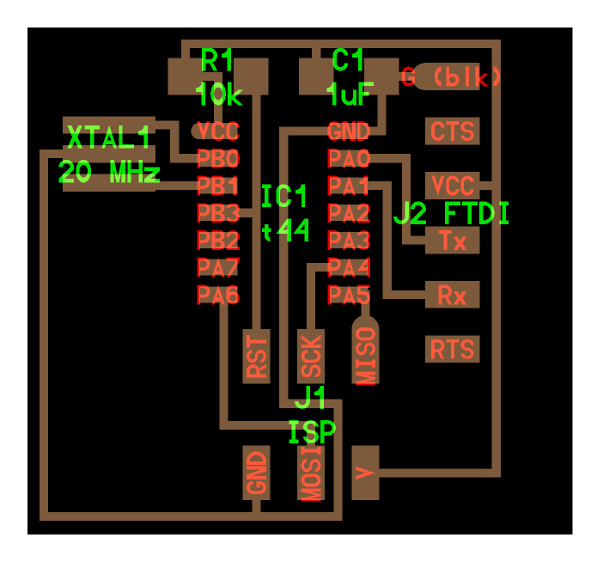
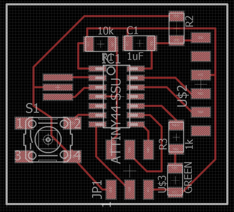
Laying out the board was an exercise in patience. At first, I didn't adjust any default settings and just went with the routing style provided in the example. I learned very quickly though that the routing example had custom parameters that made it possible to route three traces under the Attiny44 - with default settings, one of the traces would be closer than the minimum 1/64" distance required between the trace and other pins forcing it to be shorted to the entire left side of the Attiny44. Not good.
I only found this out on my first attempt to print the board. I used the Shopbot in the Harvard lab and made a few more mistakes which I will document here. (1) I've gotten accustomed to using the new fab modules (mods.cba.mit.edu) and when you load a server program, it asks you which device you will be cutting on. During my first print, I made the mistake of clicking "Roland Mill MDX-20" when I should have clicked "Shopbot image png". (2) I did not explicitly load default settings for the cut. As a result, my "traces" were cut using the standard settings for a 1/32" cut all the way through the board. I would like to take a minute to apologize to the 1/64" bit that had to deal with my incompetency on this matter.
The resulting board was not beautiful and resembled a badly maintained construction site more than an elegant fast PCB. The proximity of the traces meant the only way forward at this point was to return to the drawing board and fix what was wrong in my first version of the PCB. Back to Eagle it was...
I'm rather proud of the new schematic because it does not worry me anywhere near as much as the previous schematic did. The geometry of the board has been changed as to make it take up a smaller overall area. Instead of routing three traces under the Attiny44, I've reduced that number down to only one. The only added complexity is a 0-ohm resistor at the top of the board to jump power over GND, but that's a small price to pay for an overall more aesthetically pleasing board.
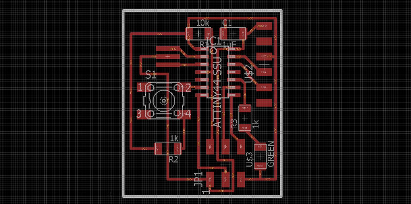
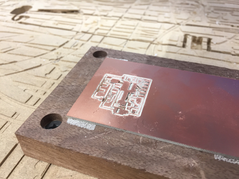
Milling the board was very easy once I had the settings correct - I have to say thank you to Rob Hart for double-checking those settings for me before I went to print. The traces came out beautifully but when I tried to cut out the edge of the board, I ran into some trouble. Fabmodules didn't like how small my edge cut was, so it scared me with a half-cut that looked like it was going to cut straight through the section of the board with traces. I stopped the cut and assessed the situation - instead of taking the time to fix the edge and attempt another cut on the Shopbot, I chose instead to minimize my losses and cut the rest of the board manually using tin snips. The edges of the board are a little rough, but the board gets the job done and is safe from any faulty attempts to cut through with the Shopbot.
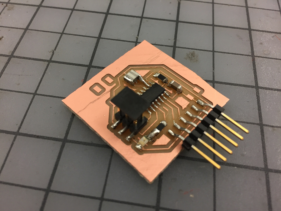
Soldering was extremely straightforward - I think I've gotten better at it over the last few weeks and can now solder the individual pins on the Attiny44 without a problem. I'll definitely try to improve this board a little more before the programming week (perhaps make the traces 0.02" instead of 0.01") but I'm proud to say the board is assembled and (as far as I know) functional!