Week 5: Electronics Design
Using Eagle to Create the Base Schematic
I chose to use Eagle for my schematic and board creation due to its use at a professional level and due to the future connection properties it has with Fusion 360 and other Autodesk products. I've only used LTSpice to do circuit design in the past and Eagle was very different. I had to figure out how ot import and use the proper library and then referred to past students' documentation to figure out which components mapped to which codes from the provided board for the assignment. My final copied schematic was pretty messy and when I tried to move the component blocks around, the lines would not move in a pretty way (they would move diagonally instead of in a nice Manhattan distance way):
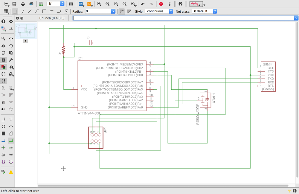
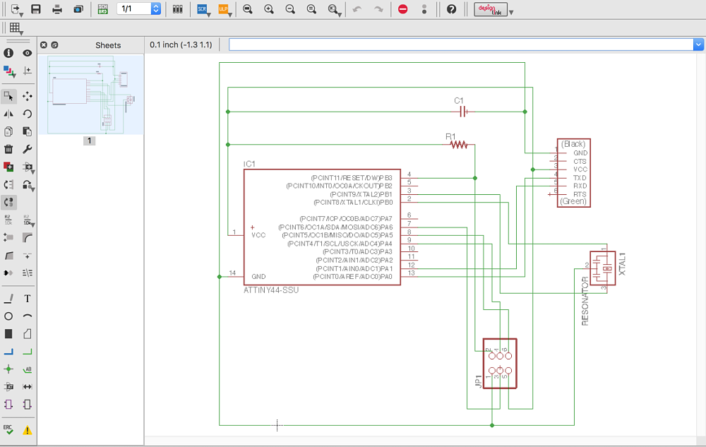
To my horror, my computer crashed and I didn't realize that my Eagle schematic did not save (for some reason, I had expected it to save automatically since it didn't have the asterisk * next to the file name at the top). This was a good lesson learned to keep checking for file saving. I recreated the schematic and noticed that it was slightly neater than before:
Adding the Button and LED
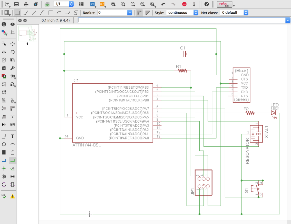
I then tried to add function so that a LED lights up when a button is pressed down. This involved first putting the "input" switch between the ATtiny and ground. I was going to add a pull-up resistor between VCC and the button input so that the current can flow through normally when the button is pressed and so that the voltage doesn't float when the button is released, but then I read the data sheet and realized that both Port A (PA7:PA0) and Port B (PB3:PB0) have internal pull-up resistors. So I just put the button between PA7 and ground.
For the red LED, I added a current limiting resistor in series (between output pin and ground) so that the LED wouldn't explode. For a 5V VCC and for ~5mA to pass through the red LED, by V=IR, I added a 1k resistor. I connected this to PB2 since it was the only Port B pin remaining. The final schematic looked like this:
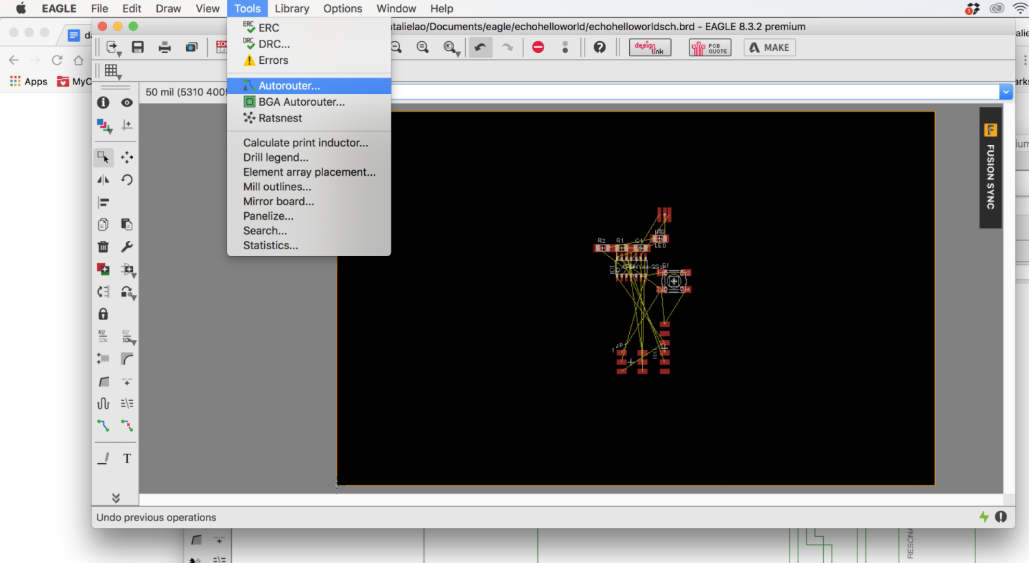
I clicked the "Generate/switch to board" button in the top bar to create the board. I imported the design rules from an alumnus of the class and then tried to autoroute, setting the top and bottom layers to "Auto" and the other layers in-between to "N/A".
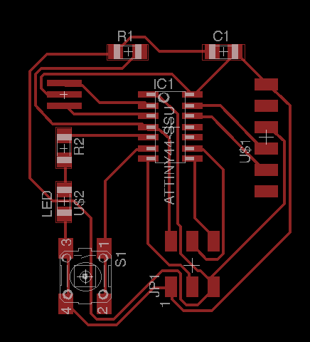
I had to RIPUP; and reposition the components on the board a few times before the re-router was able to find a workable set of routes. I saved the monochrome board image with only the Top layer showing through View -> Layer Settings and then used preview to draw the outline.

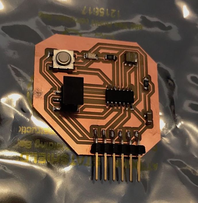
Milling and Soldering
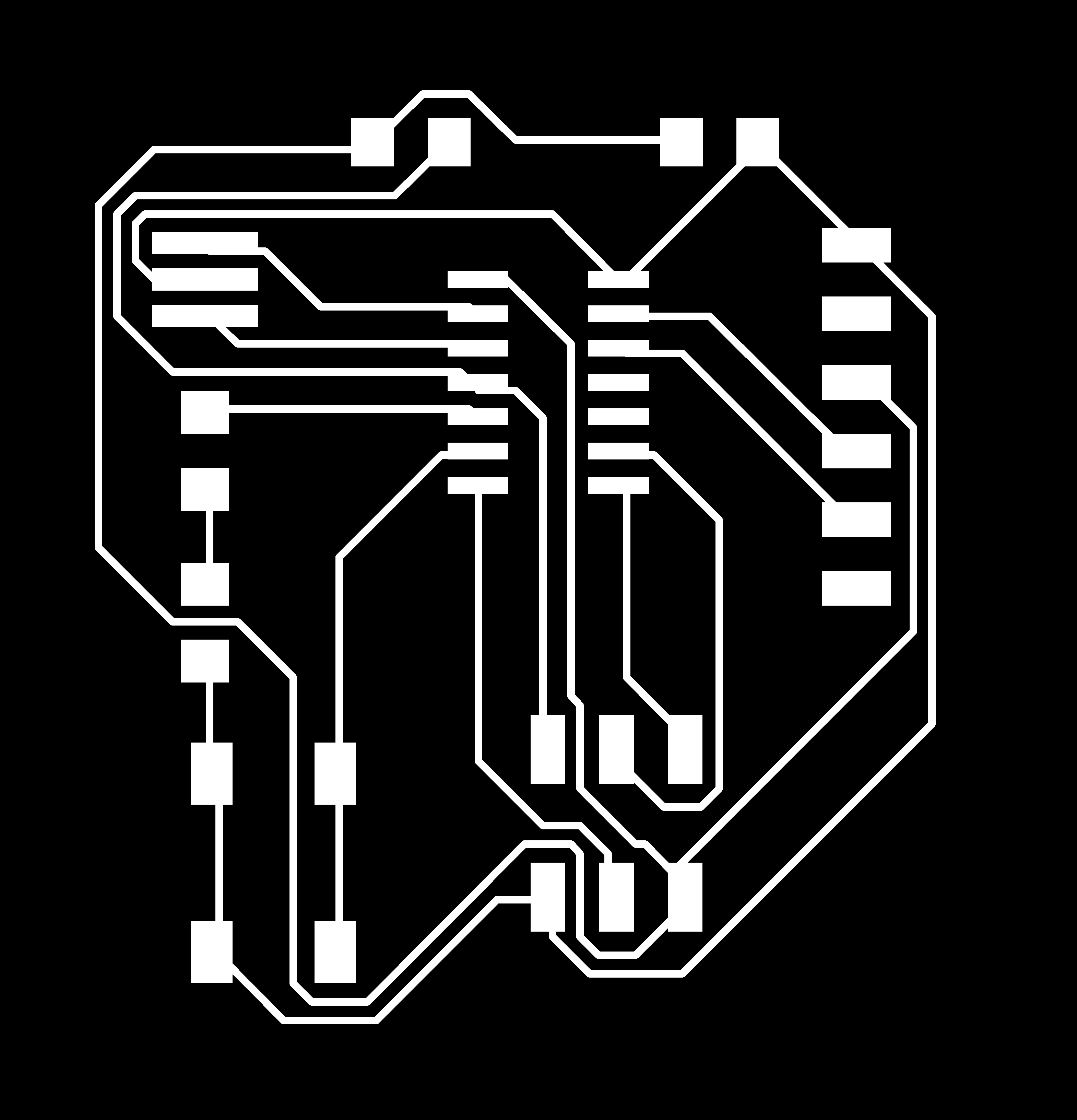
I changed the cut depth to 0.005in because the 0.004in default for the 1/64 bit (traces) did not cut deeply enough. I also had to double the DPI because it cut double the appropriate size. When I cancelled the job due to these issues, the machine wouldn't start up again, so I had to power it off and then on. I also changed the device from lp0 to lp1 and tried using the sudo node /usr/local/bin/printserver.js 127.0.0.1 1234 command in terminal. When I tried to mill the PCB, it only cut the corner edges because my black image was just on a blank background. I had to put a white background and add some borders to my image:
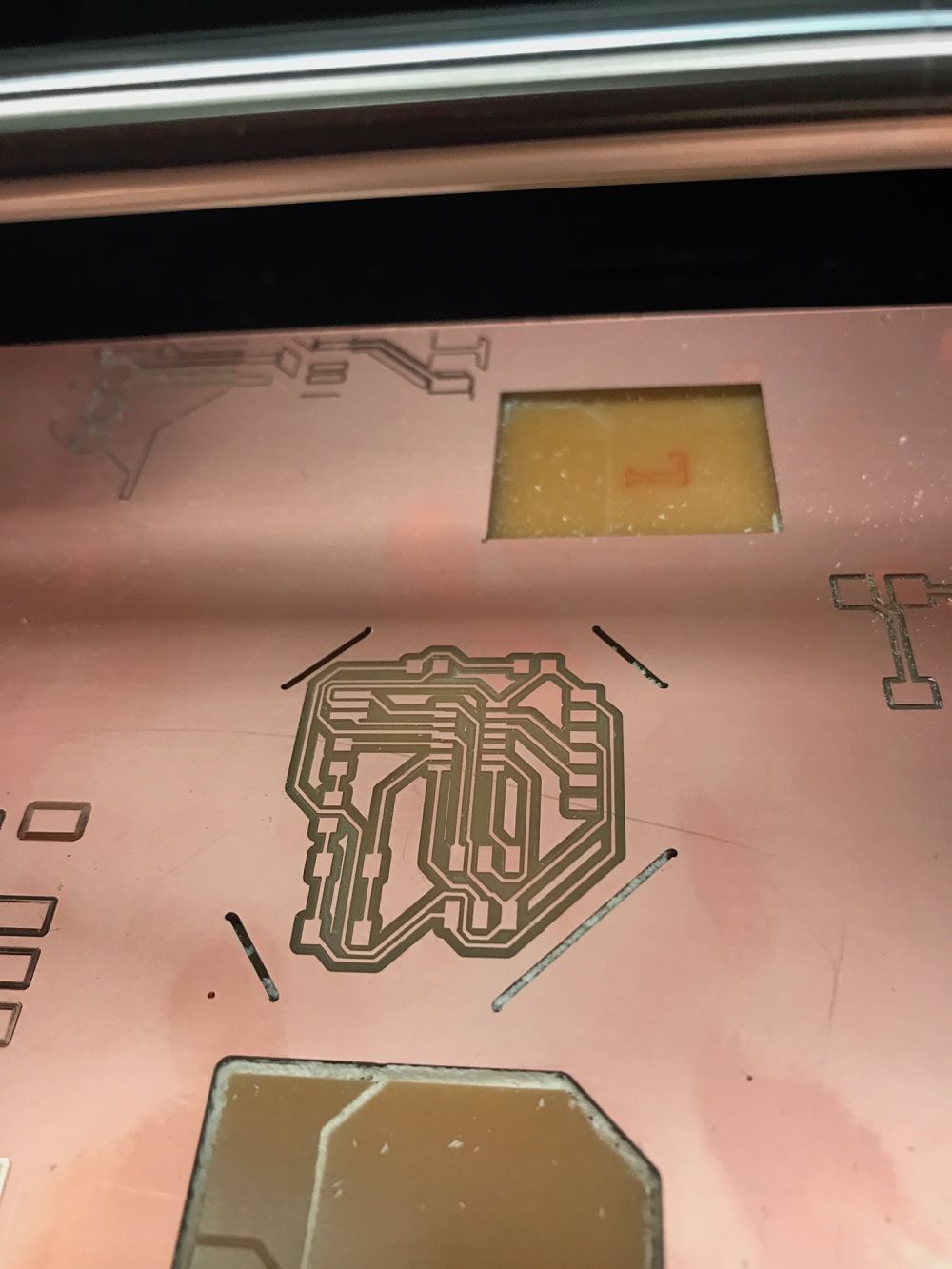

The second round milled the whole piece. The board shifted a bit in the process, so the outline was slightly offset, but none of the traces got cut through and it still turned out to be workable.

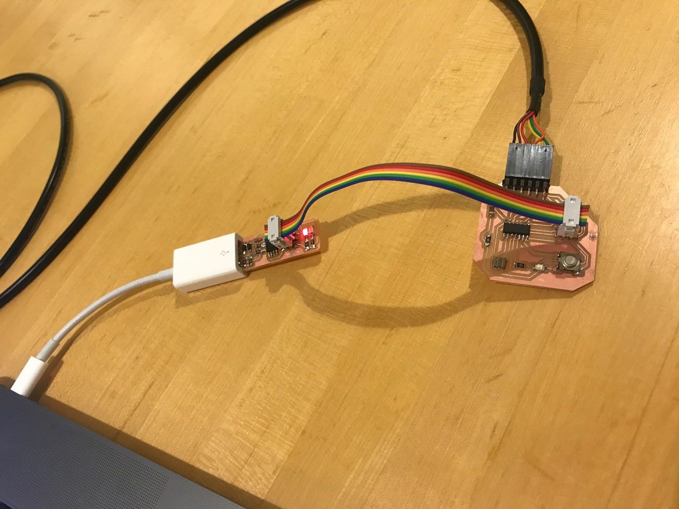
I hand-soldered the components onto the board:
Programming
I loaded the default program from Week 3 on the new board using the first programmer that I made: