Week 4 - Circuit Board Design

Designing a hello.t412.echo board

My first goal was to just redesign the layout for Neil's existing hello.t412.echo board

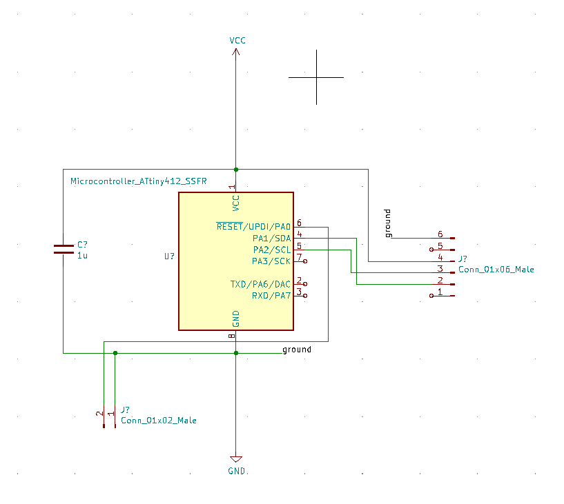
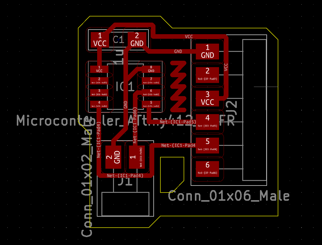
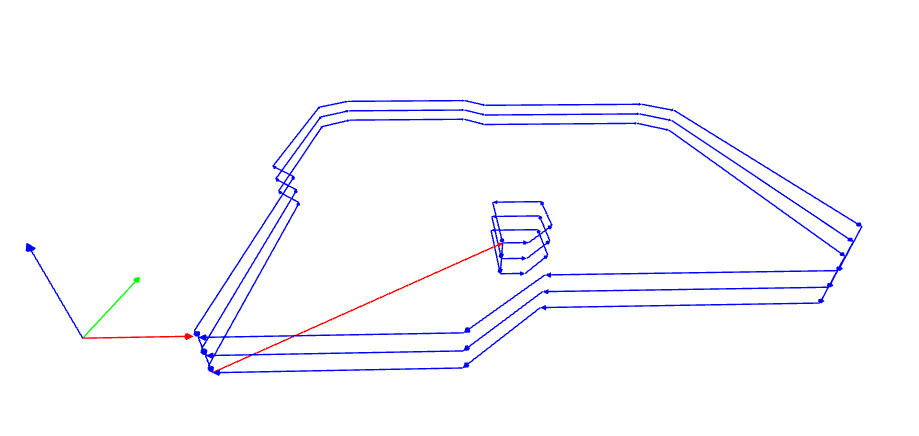
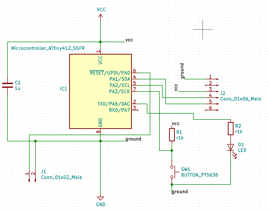
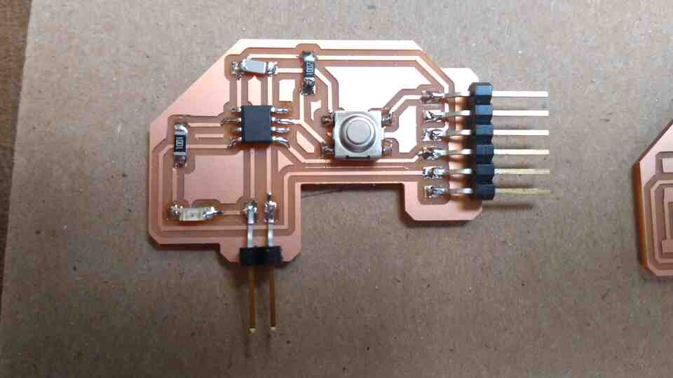
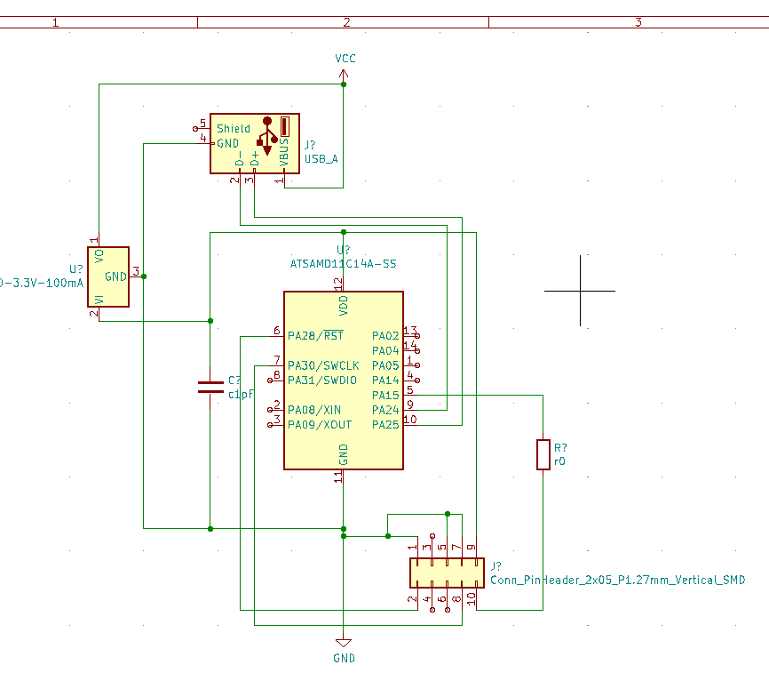
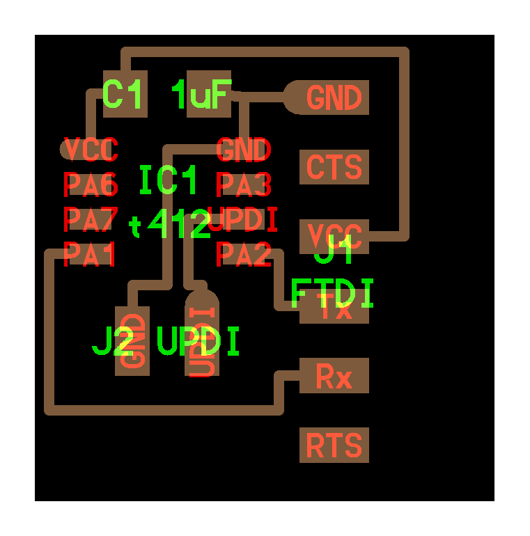
Using attiny 412 microcontroller and Neil's design as a guide:

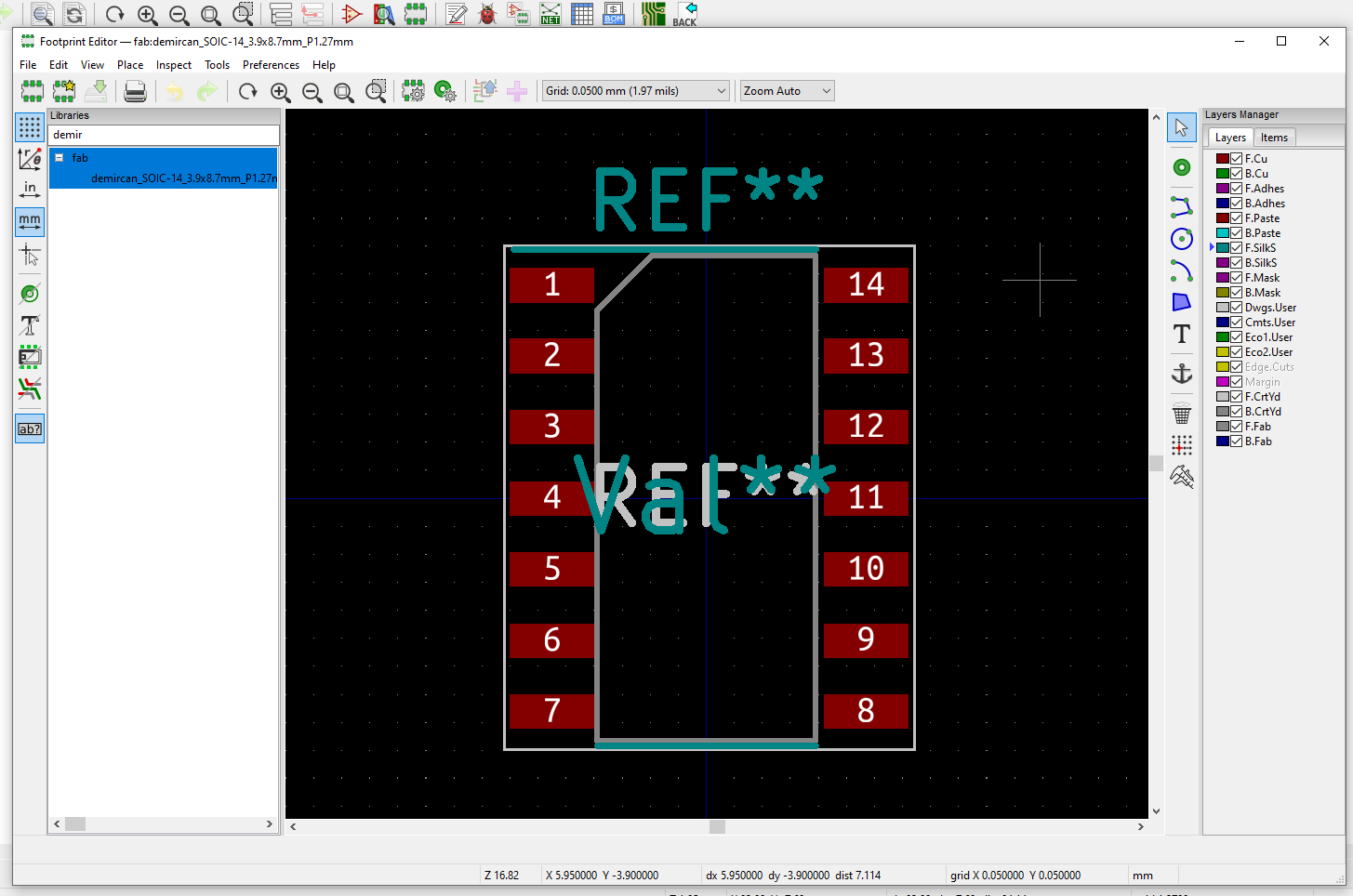
  • I created schematics in Kicad,
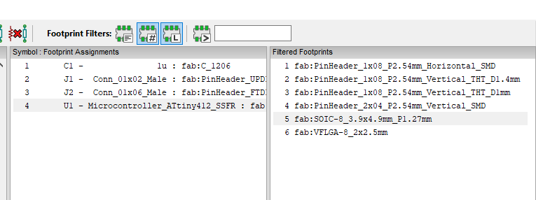
  • matched them to the footprints from fab library,
    • Some people had problems installing the default footprint libraries that are necessary for a VCC footprint. I have managed to isolate the default libraries and uploaded them to this directory for troubleshooting. I'll keep this link up for a week. If you need it after that, just contact me.
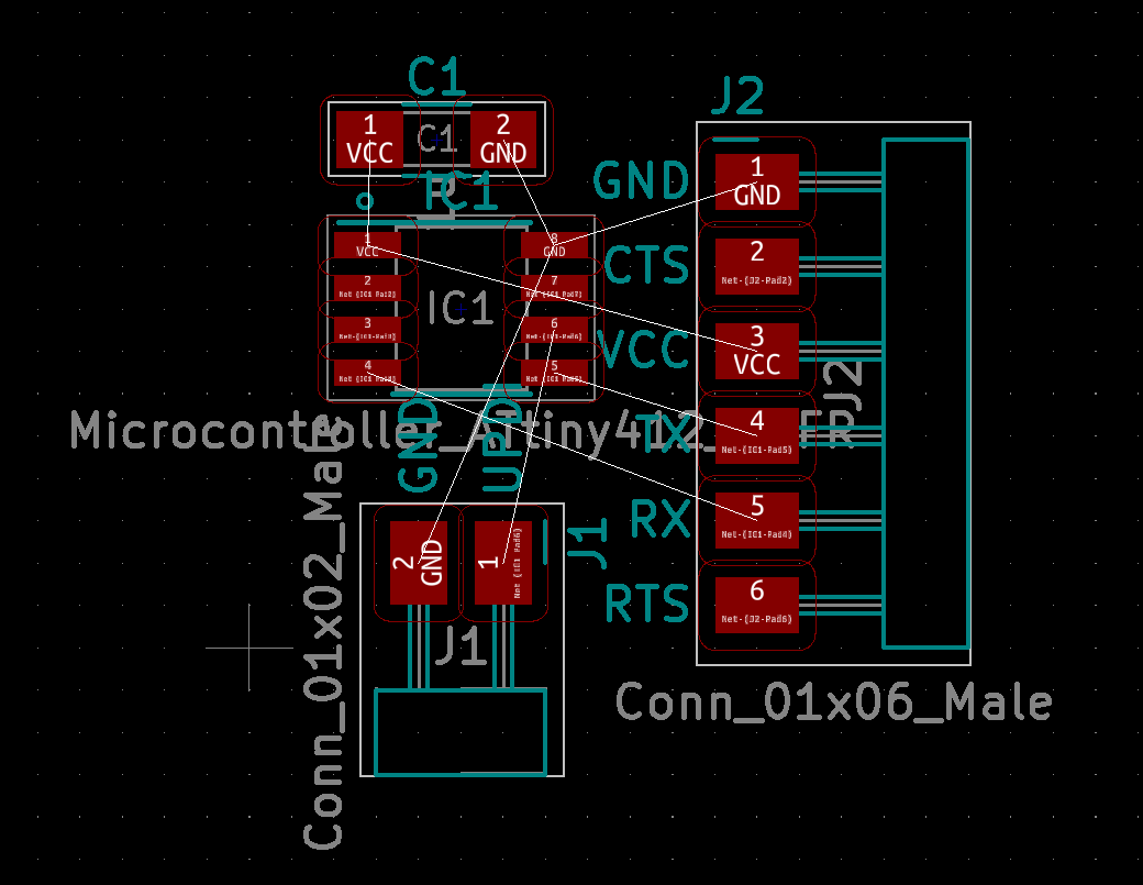
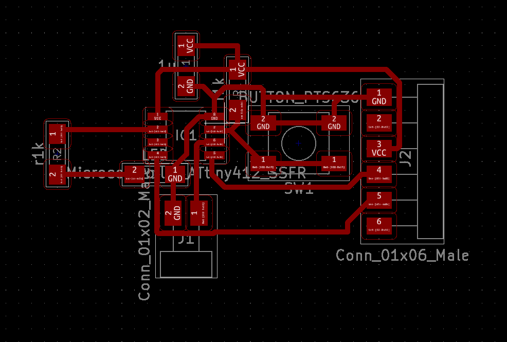
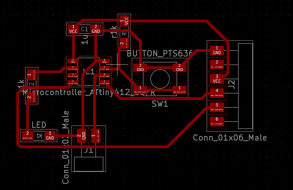
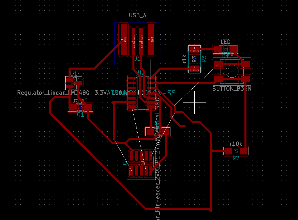
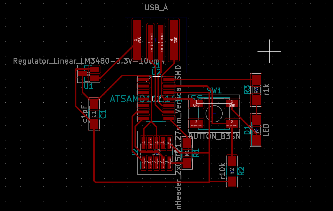
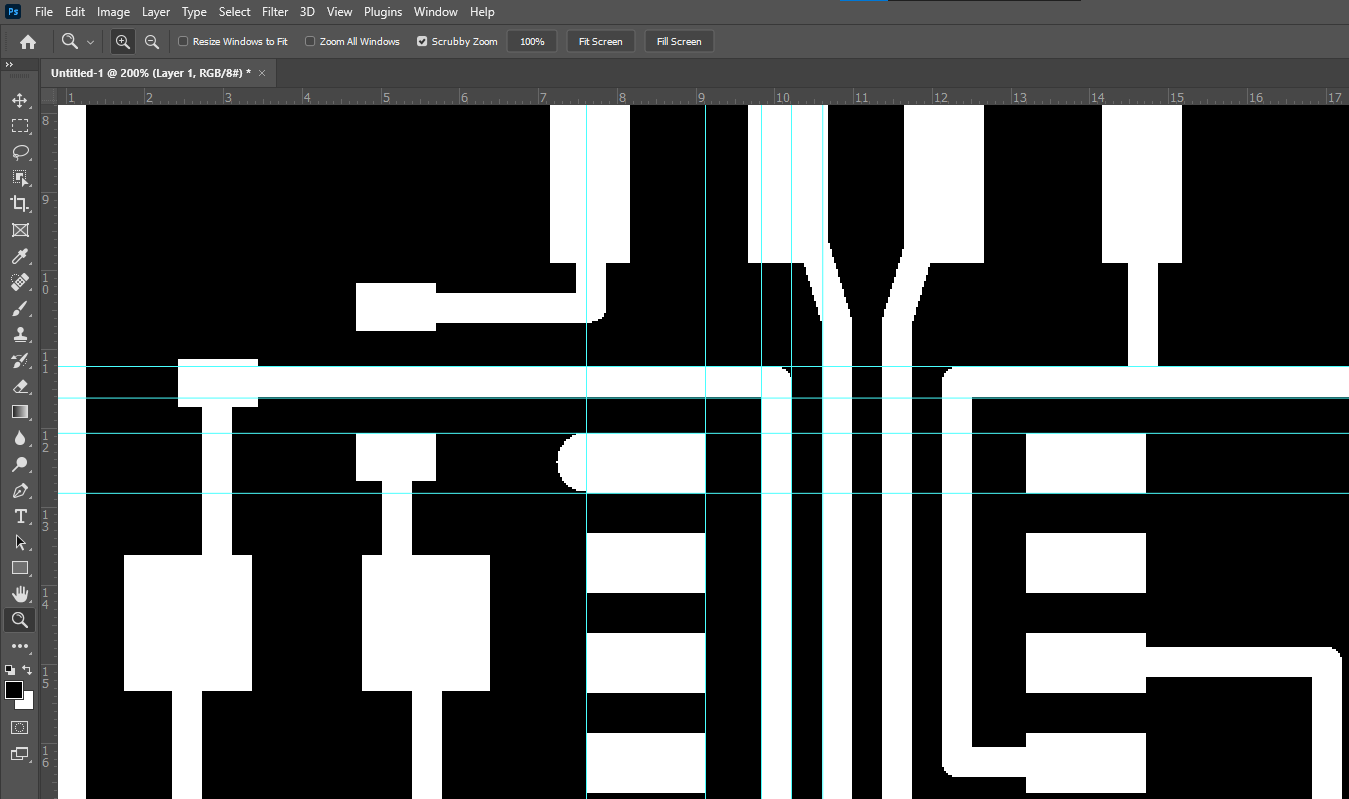
  • exported NET file to the footprint editor,
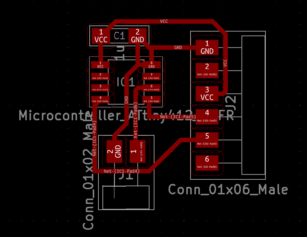
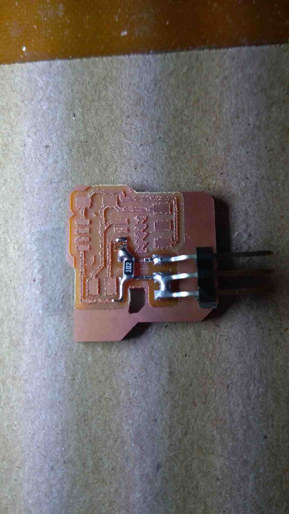
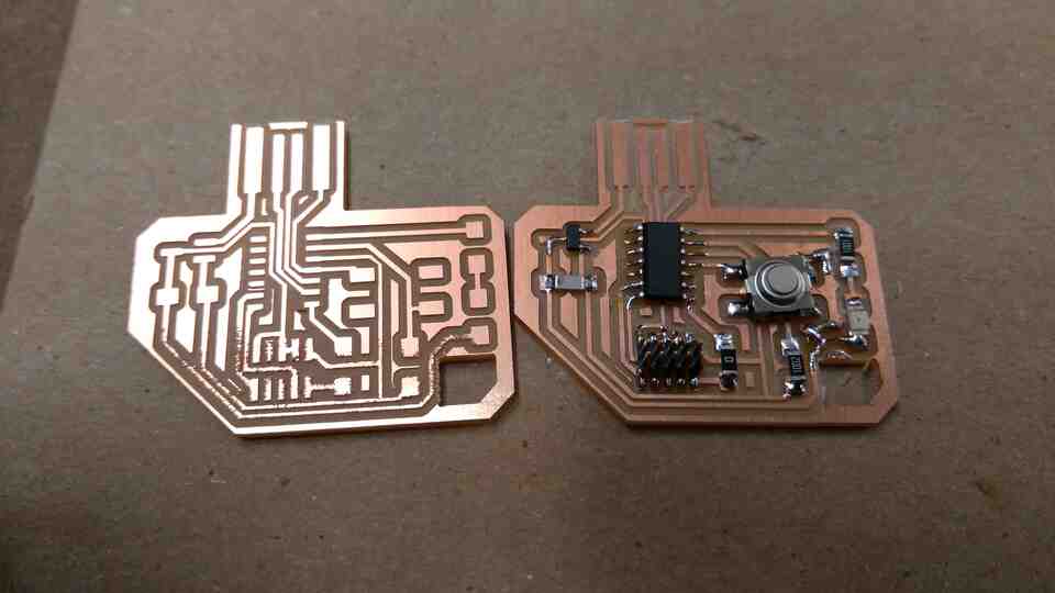
  • routed each component,
  • and created a border polyline for outline cuttling.
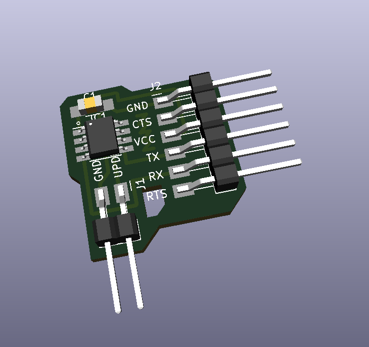
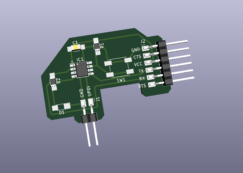
  • If you press alt-3 Kicad provides a cool 3d model view.
schematics schematics schematics schematics schematics schematics
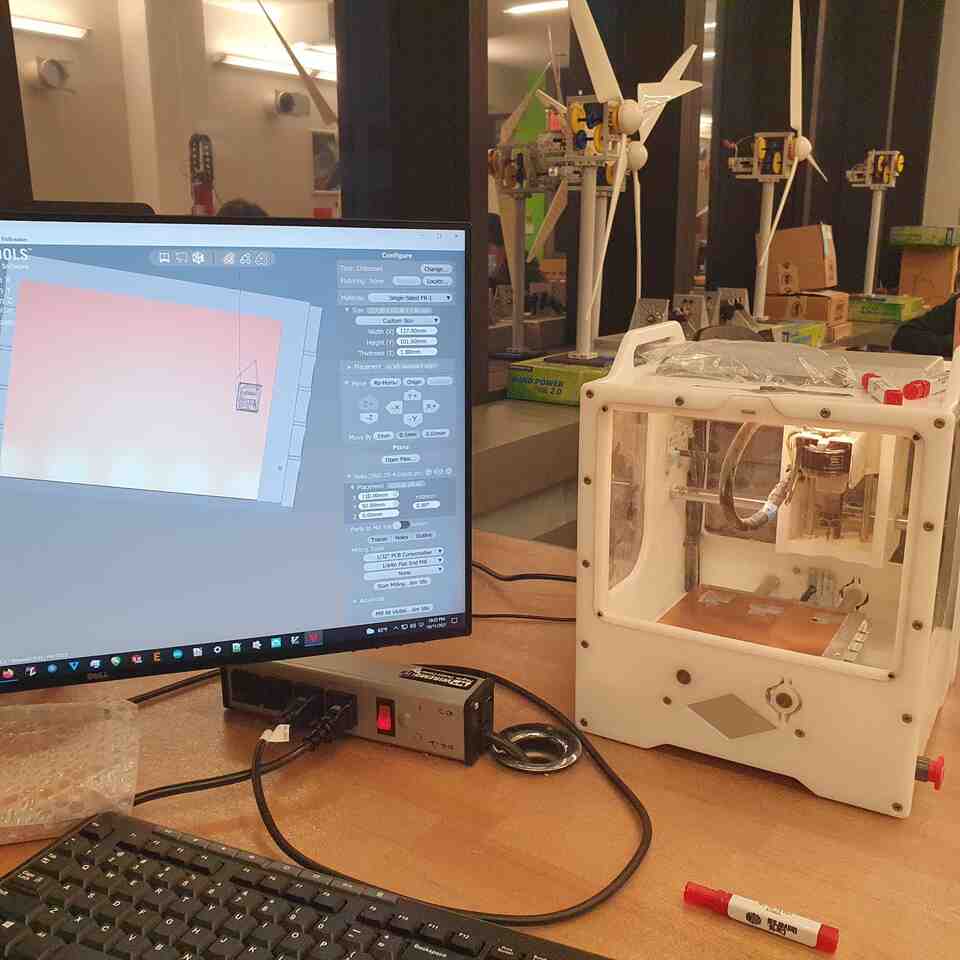
  • Kicad can export SVG files which need some tweaking in Inkscape before sending to mods for cutting.
  • Remember to invert SVG in mods (this is tedious in Inkscape).
schematics schematics schematics
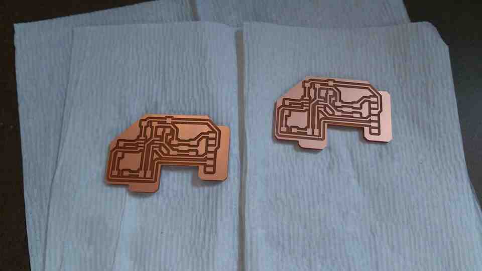
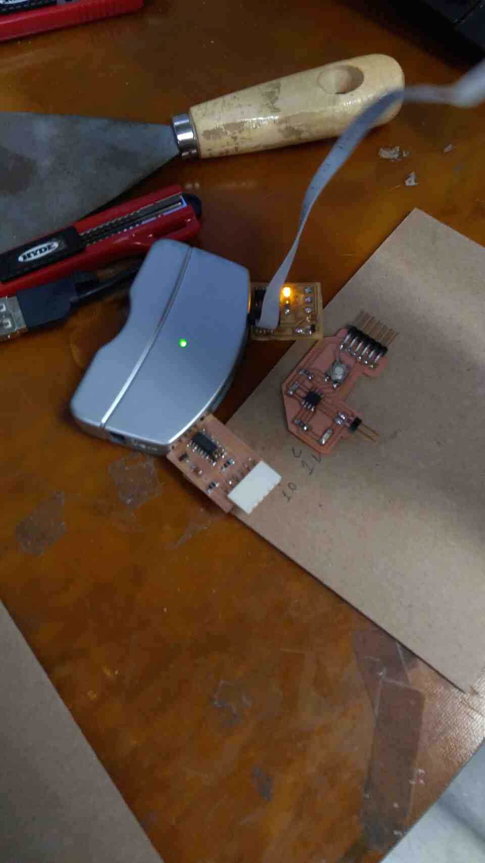
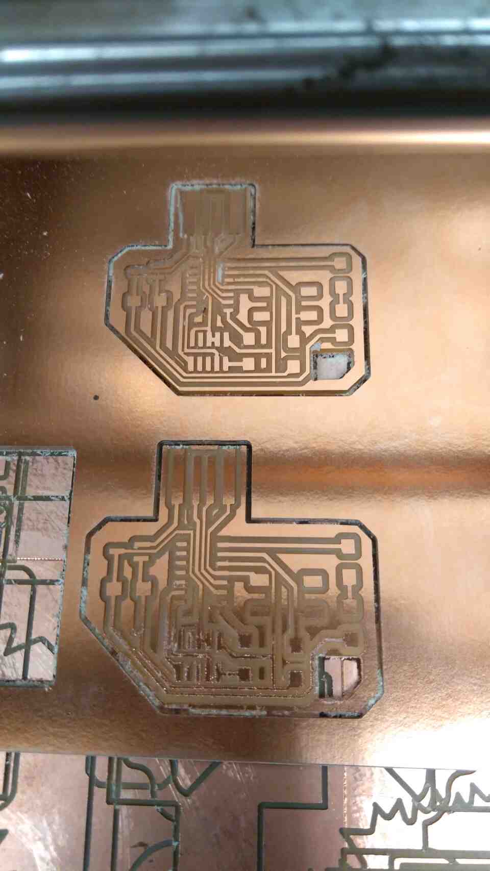
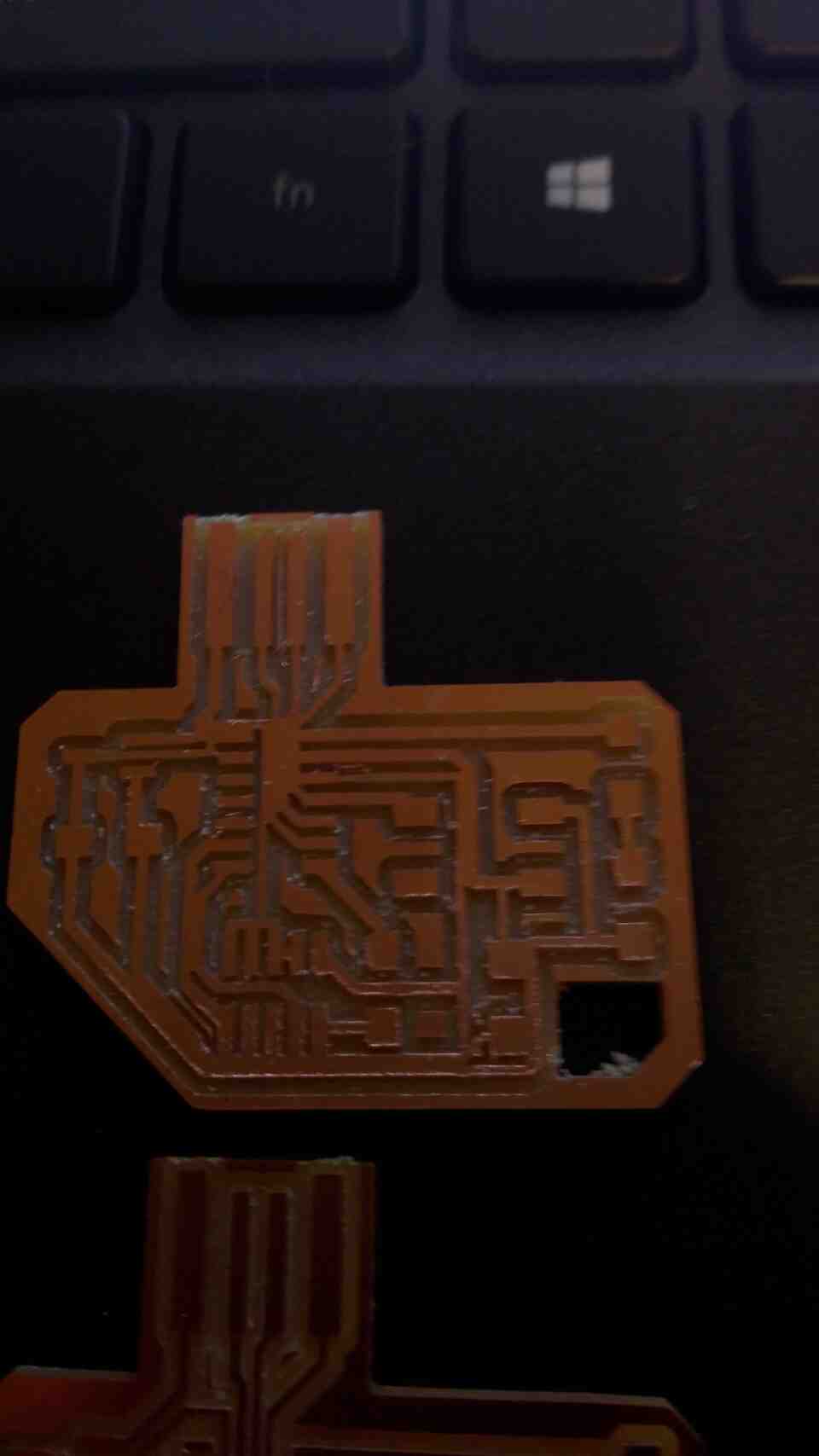
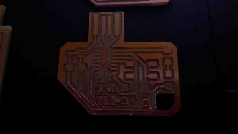
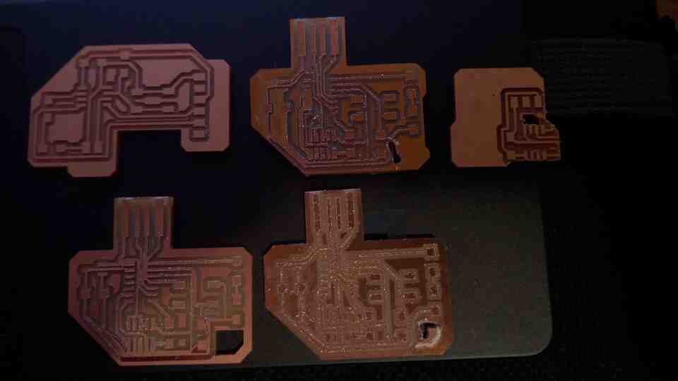
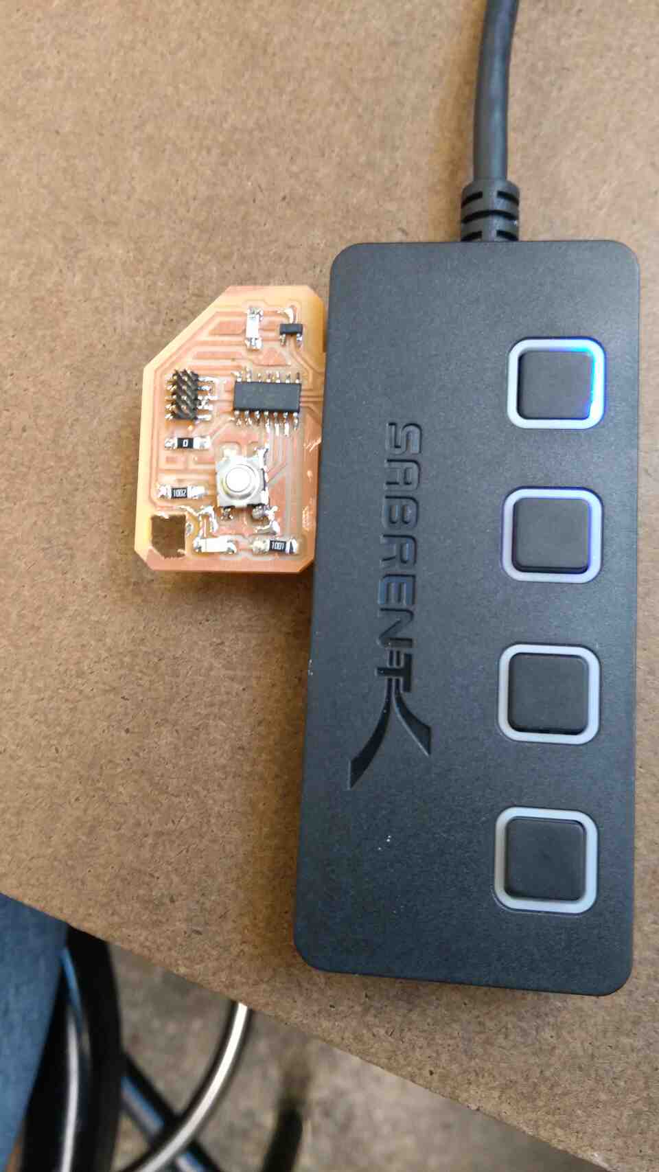
  • In the first outline cut, the Roland SRM20 had a blinking failure and we had to restart it. Following the restart, despite checking the origin values in Mods, the origin was offset by almost 1cm.
    failure
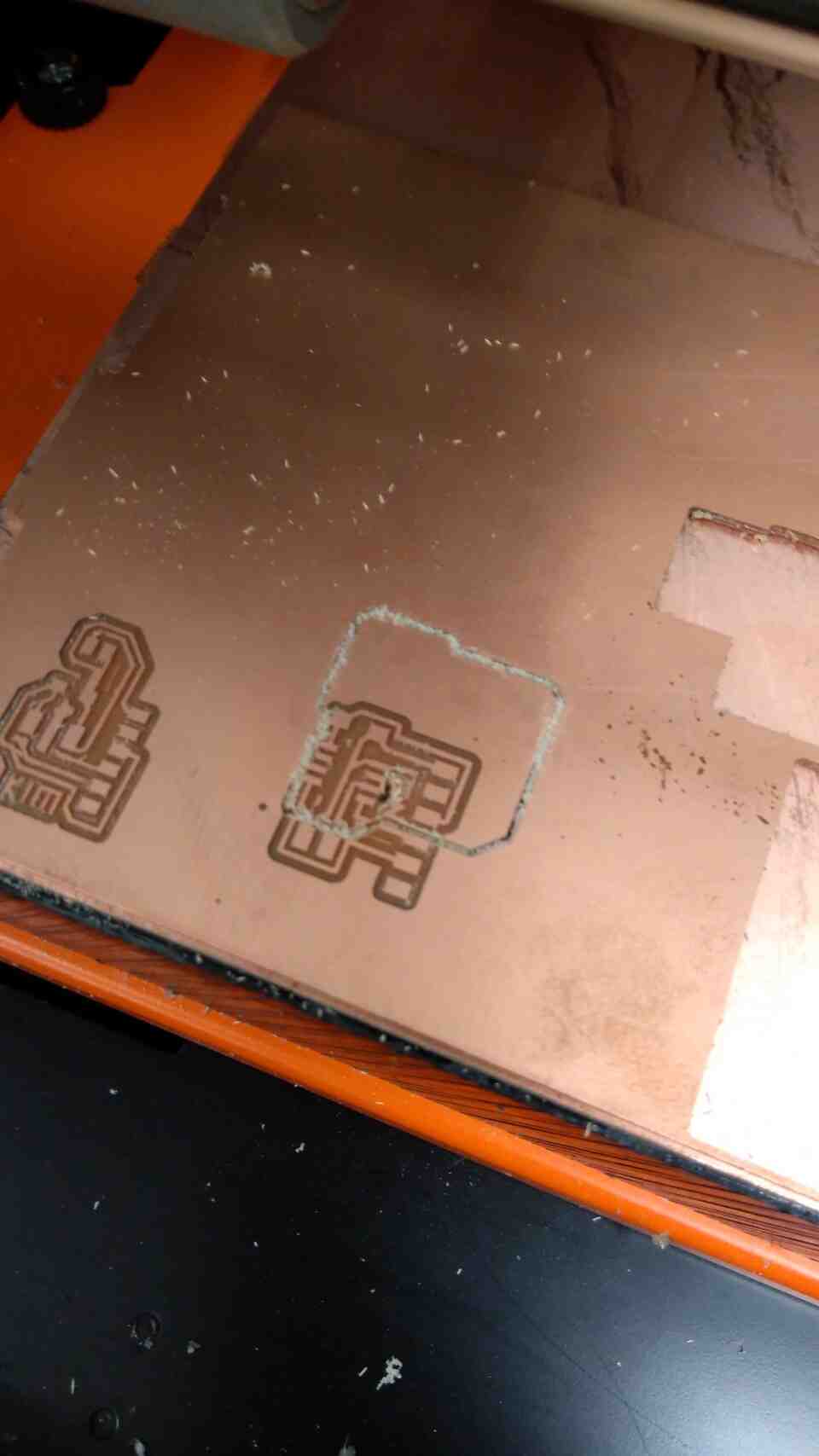
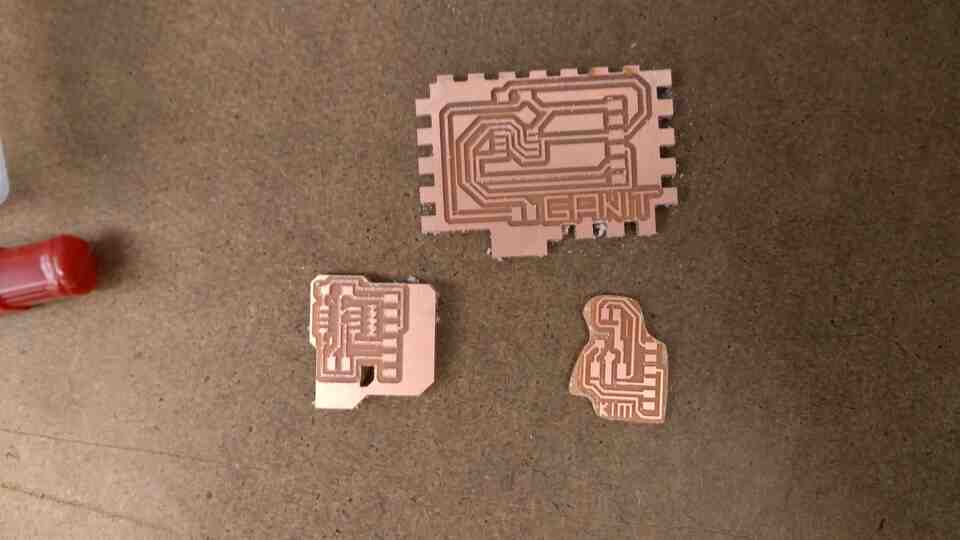
  • The next cut was fine with minor variation in quality between Ganit, Kim, and I (with the same settings and endmill, probably due to a non-flat bed).
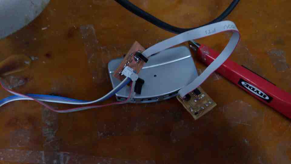
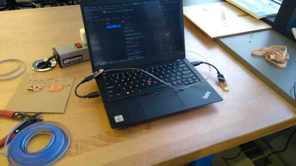
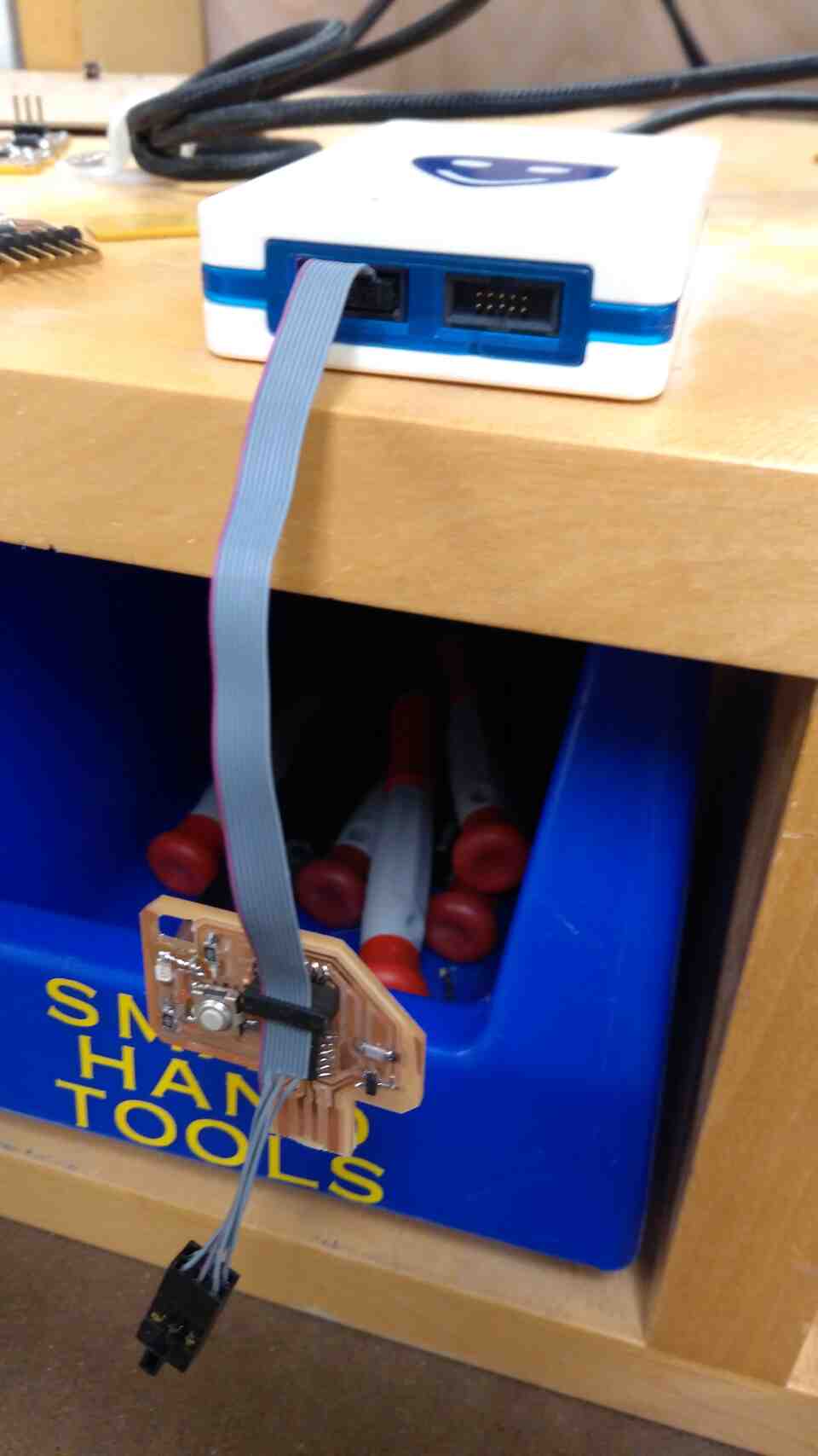
  • Jake shared some insight on the oscilloscope, which may come in handy once we program our boards.
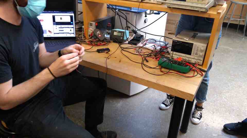
  • One extra useful thing is the voltage source next to the oscilloscope.

When the PCB was done, I went for the new design, which I would also solder.

  • Initial iterations for the button & LED
  • First cuts were eventless, so I went directly to soldering components and shimming.
  • With a board, I went to the CBA shop to get a program in, but we were lacking the necessary intermediary boards. Zach helped install a bootloader for the D11C from the previous assignment, but we were unable to program the Attiny412.
  • Moreover, the D11C did not function in the USB port.
  • Zach pointed me towards this pyupdi website, where I followed the schematics to create a serial cable that would hopefully provide a means to program the Attiny without a programmer board. I could not get this to work, but had some extra soldering practice.
  • On Monday, I went to the EECS shop to program my board. But we could not get any of the boards running.
  • Anthony and Harrison provided some great advice on connector shapes and creating cable connectors.
  • Decided to put the Attiny412 on hold for now, and create a new board: D11C with a USB.

On Kicad, I tried to mimic Neil's layout for hello.D11C.echo.

  • On Kicad, with the recitation settings (0.5mm cut and margin), it was not possible to fit 3 lines between the microcontroller legs, let alone 4. And lowering the margins was not a great idea.
  • Upon examining, and measuring Neil's PNG at Photoshop (with the right DPI), I figured he had 0.4mm tracks and gaps. Having 4 lanes in between the microcontroller legs was not possible with the footprints in the fab Kicad library.
  • I created a custom footprint file for the D11C (link at bottom), that allows fitting 4 lanes under the chip.

Here are some of the failures from this week:

And the finished board with components and goofy fixes, because I forgot to trace one connection in Kicad.

On the dawn of the fifth day, we (I mean Laura) have finally managed to get both D11C's programmed. Boards need a bootloader pushed via EDBG, and programs sent via Arduino IDE. However, many things can, and did go wrong during the process.

Now both DC11's echo. However, one of them only works with the 2x5 connector tied to the programmer.

Special thanks to Laura, Harrison, Zach, Jake, and Anthony for putting up with our endless questions and issues through this rough yet fun week.


  • Do not forget to plug boards to a power source when programming.
  • All shops are a little different, a great opportunity to test new tools, meet cool people.
  • Always check solders with a voltmeter.
  • Don't rely solely on existing libraries.
  • Peel excess copper by rotating the tweezers, and enjoy!
  • Go for the tools that people do not use (Unless you like to sleep at nights).
  • EECS shop has a sweet and smart PCB milling machine, with great results.
  • Do not yank connectors when they are stuck.
  • Failed boards come in handy as weird hacks.
  • Media Lab folks know how to party.