Week 4- Electronic Design
Routing rerouting rerouting

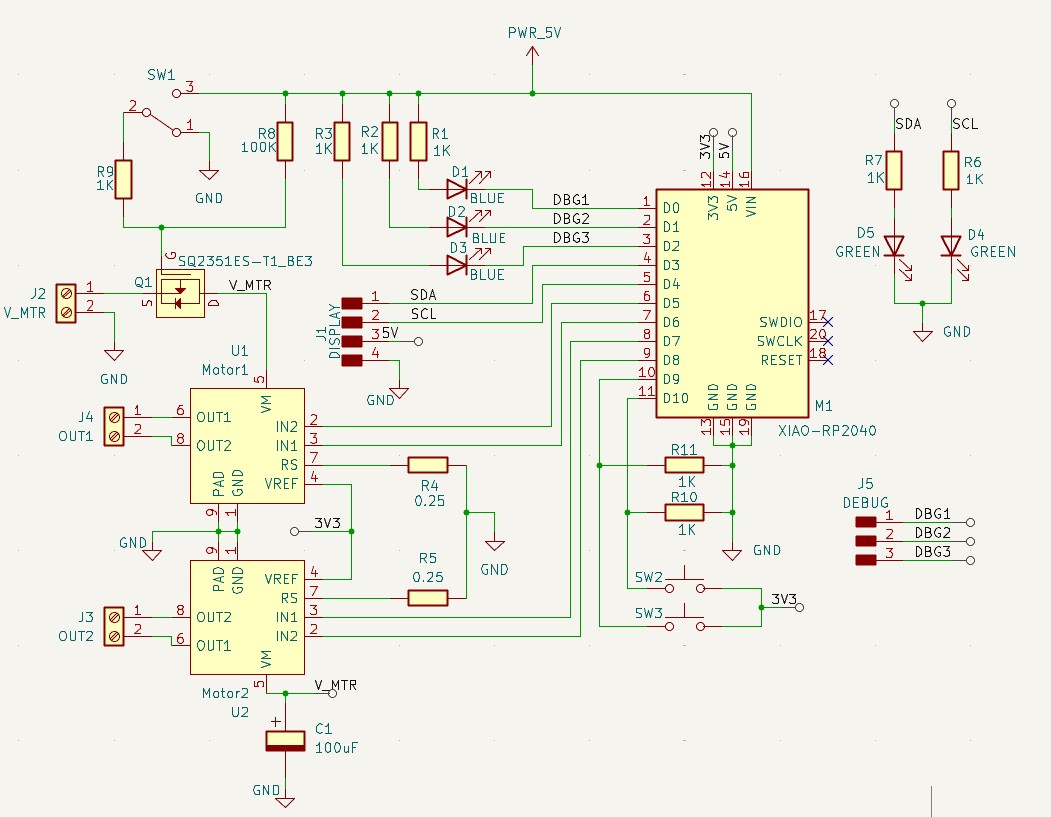
This week we did some electronic design. This is probably one of my favorite things ever. It takes some patience to do it, but I truly think it's relaxing and calming. For the design, I decide to make a motor driver. My final project will use DC motors, so I thought I could start testing some of the logic. So my deisgn would mostly be two H bridges to move two different DC motors. When making any eelctronic design, the most important thing is to check the datasheet. There truly is nothing as imperative as the datasheet. Back in my undergrad, I had a microcontroller class in which we used the PIC16F887 and programmed in Assembly, and we all printed the datasheet as our textbook. That class truly hammered in the lesson that datasheets are the bible for EE and truly try to live and breathe datasheets.
But I digress. The thing is, I looked up the datasheet for TB67H451FNG driver that I am going to use. I check the connections, but I especially check if it needs any additional components. On page 10, I see it is necesary to calculate a resistor we are going to use to limit the current. Ideally it would be a small resistor, but the exact value I calculated is not available. The smallest in the inventory is 0,25 ohms, so I went with th.
I used KiCAD to make the design and PCB. I've only used Altium before, but in the end they're not that different and I managed to adapt. I lost access to Altium long ago, and it is too expensive to use as an individual, so I am thankful to learn a new tool that is opensource and free.
To be completely honest, I zone out an locked in and forgot to take more screenshots and suddenly it was done. But I will continue to break it down here.
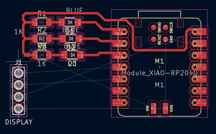
I will go in the order of the pins for the Xiao. We strat with the upper left corner. In this one, I have three pins - D0, D1 and D2 - serving as debugging pins. I added LEDs that will turn on with a digital pin on LOW to help me visualize any errors that might happen in my code. It's sort of like printing things in the serial monitor, but I find it easier to just see a light turn on. The next D4 and D5 are the I2C communication pins- SCL and SLA. They get connected to a pull-up resistor going to 3V3. (Foreshadowing- I did this wrong, it was D5 and D6). The picture up there is the final fixed design after realizing this on the following week. Then we have D6 and D7, which are the two pins that will control one motor. D8 and D9 will control the second motor. D10, D11 and D12 are digital inputs connected to pushbuttons. Then we have the power pins. 3V3 goes to LEDs and pushbuttons and the source of the drivers. GND goes to all GNDs. Then we have 5V, which goes to the display. The motor, however, are powered by an external 12V supply and go through the H bridge. The terminal blocks are to easier connect and disconnect the cables for the power supply and both motors. This 12V is connected to a mosfet, which is manually controlled by a switch that will turn on or off the power to the motor drivers. This way, they cna be powered off when not in use. The LEDs and buttons are mostly to add inputs and outputs for testing purposes. The OLED Display would show the motor speeds and everything.
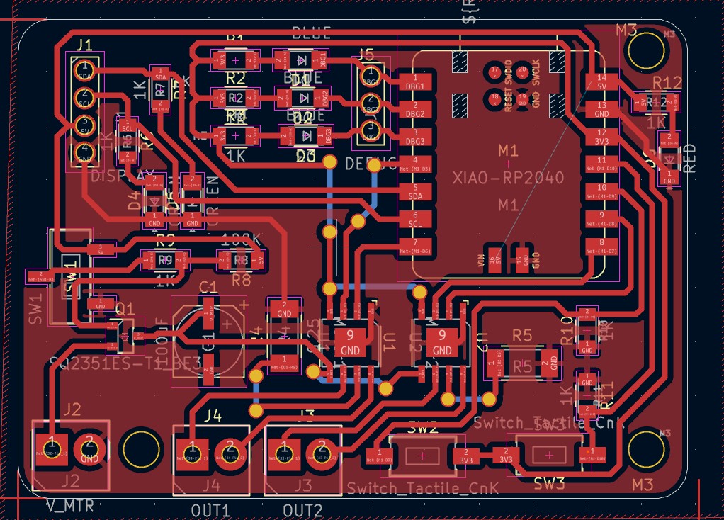
In terms of PCB routing, I always try to keep it as compact as possible. For this purpose, I first roughly choose the positon of all the components that would have a restraint, such as the xiao package, which requires a USB connection and therefor that edge must be on the edgeof the PCB.
The terminal blocks also need to be on the edge for easy access. The pushbuttons need to be in a spot where they can be pushed without being uncomfortably close to other components. The rest of the components I just try to group them by function and keep them as close as to their route. This means I will drag them around and rotate them trying to imagine how the routes will look. I also reference back the schematic to see which components have more connections and try to keep them more central. Since I chose the pin numbers in order, it is easy to related components in order as well. Routing is an art and I just enjoy putting the traces in parallel lines and making it look nice. I try to avoid the 90 degrees angles and I avoid vias as much as possible.
However, it is hard especially when using ICs like the H drive that just has a lot of pins and theres no clean way to route them all without needing the traces to overlap. Thats where vias come in. However, I did not want to eventually mill a double sized PCB, so I tried to minimize the vias as much as possible. In the end, I only neeeded 5 jumps to the bottom. I could not use a 0 ohm resistor as a jumper, as my overlapping traces were often going through several traces with very little space. I planned then to use cable souldered from the vias to the other vias. I modified the vias to have a much bigger diameter.So that's my board, I'm happy with the result and look forward to machining it.
Here are the files: schematic, and PCB.
note: I tried simulating but I couldnt find the same H bridge in any of the programs, and I thought it was not helpful to simulate an LED.