This week we are fabricating PCBs for embedded microcontroller systems. This is a process that I see as having four components:
Designing
the board in a CAD software, starting with a schematic and moving to a PCB
Milling
the board using a PCB mill machine, which removes copper in traces to create electrical connections
Soldering
all of the peripheral components and other parts onto the milled PCB
Testing
to see if any of the above actually worked!
Of course, spiral development would dictate testing at every stage of this process. In the case of PCB design, based on our discussion in Recitation this week it would seem that visual inspection is the primary mode of that testing. This includes checking the PCB design visually alongside the design rules check in CAD (Fusion in my case), checking the toolpath in mods to ensure that there aren't conflicting pathways for the mill driver, and checking the mill software to make sure that the traces look right for the tools.
Design Rules and Board Submission
Our first task this week, as with any digital fabrication process, was to assess the design rules of our PCB mill. In the EECS shop, we have an Othermill PCB printer which we generally use with end mills of 1/64" and 1/32".
To test the minimum trace widths, we printed a test board:
And discovered that the minimum width that the mill could execute consistently was about 10 mil. While smaller traces did technically work in the test, they were easy to break or rub off with a fingertip, making them insufficient for production.
Theoretically, the mill can accept .brd files from Fusion, but the more comprehensive and dependable way to transfer these files is as Gerber files (which have a complete set of differentiated manufacturing layers). Our section used Gerber files to submit a board design to the JLCPCB online platform and place an order. More information on our group assignment is available here.
Making a Microcontroller System
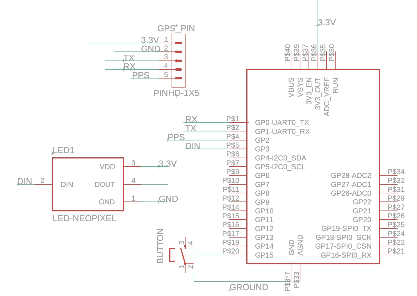
This week, I wanted to make the basis of a board for my Final Project, which I have continued in Week 8. This board has a Pico-W microcontroller with pins corresponding to a button, a neopixel LED, and a GPS module. At Anthony's suggestion I have included additional multipurpose pins to make it easier to add more components later.
To design the PCB, I started in Fusion with the diagram I produced in Week 5 and began to modify the PCB representation so that it could be milled effectively. Here is the schematic I started from:
In order to prepare this for milling, I needed ot focus on the PCB representation and ensure that the routes and clearances were ready for fabrication:
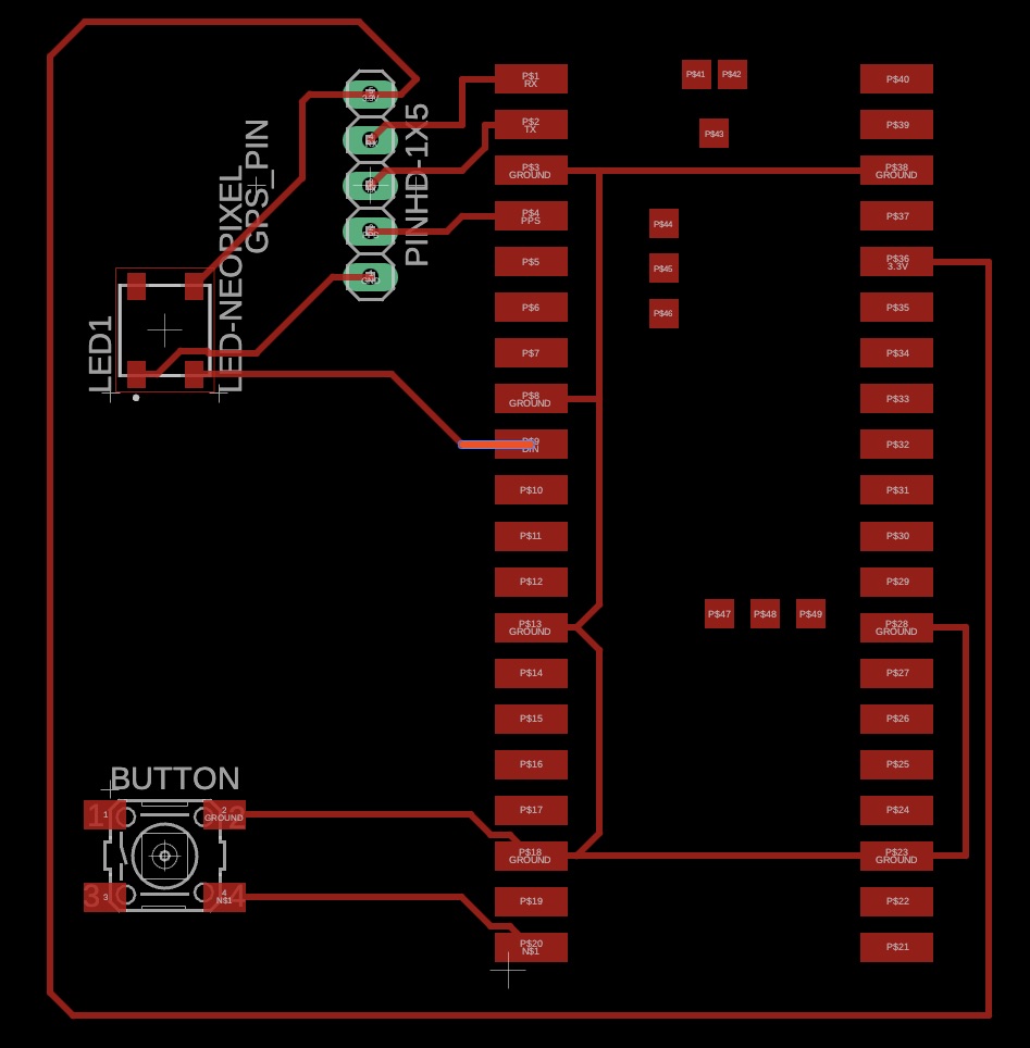
I started by adding more pinheads connecting to key pins like 3.3V, GND, and TX / RX. This was a future-proofing measure to ensure that I could connect further components to the board without having to reprint it (hopefully). I pulled these pins out of the Pico and added traces to connect them:
Next, in order to make sure that the board would mill and connect well, I made sure to avoid harsh angles in my traces and to connect to pins in straightforward ways. For doing this, it was helpful to go back and forth a bit with the bantam tools interface, to see where things were too narrow:
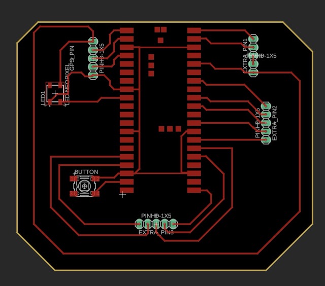
In the end, I was able to configure the board so that it could be milled entirely by the big toolhead, avoiding the need to switch them in the middle of the job. Here is the final board design, including the board edge polygon:
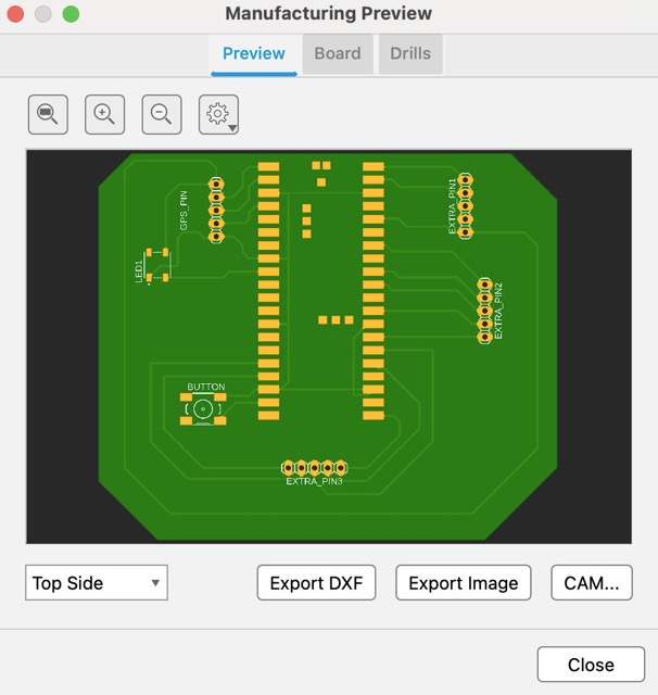
Fusion also gave me a convenient CAM preview of it:
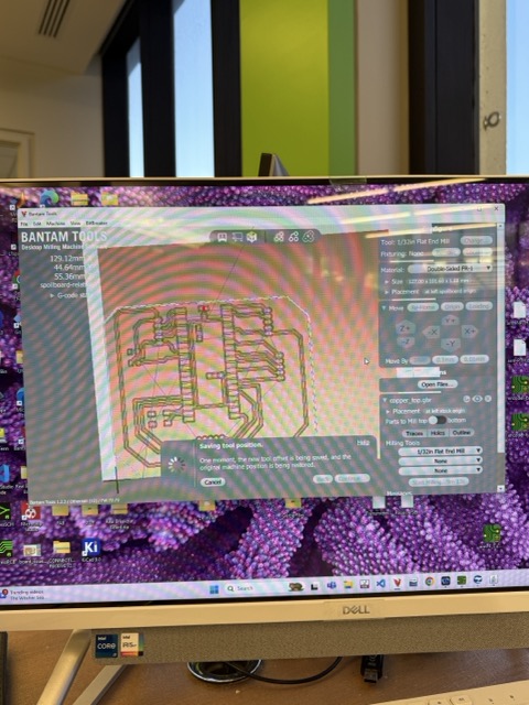
I submitted this to the bantam tool as a Gerber file because it wasn't reading my .brd correctly. For those confused by this in the future: make sure that you bring in the file and visualize the TOP of the board, so that you can see all of your components before printing!!
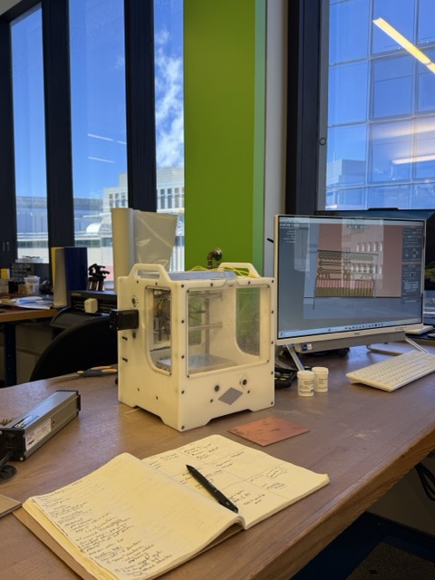
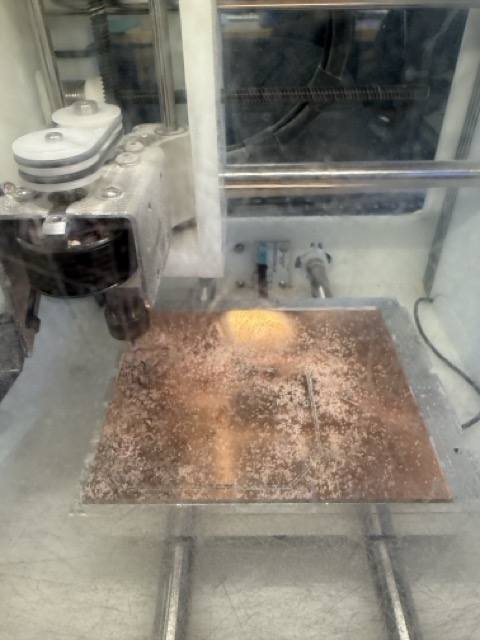
Finally, I was able to mill the board after getting the visualization on the bantam program right. I loaded the machine with a single-sided copper board and stuck it to the machine bed with double sided tape. I made sure to use the 1/32" end mill. The job took about 9 minutes:
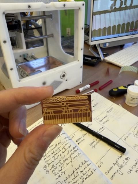
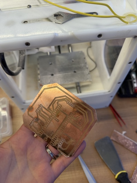
Here is the finished product:
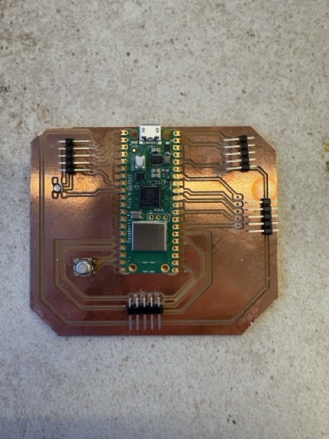
Next, it was time to attach components. I laid out a set of pins, a button, and my Pico W microcontroller on the board to show where they would go. Unfortunately I was never able to locate a neopixel LED of the right size for the pads I had cut, but it wasn't an issue at this stage because the Pico has a built-in LED.
To start, I only soldered on the Pico and the button.
Testing my Microcontroller System
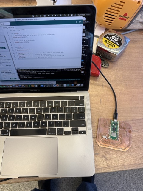
In the interest of spiral development, I wanted to test the most basic components before adding any more, so that I could identify any problem in my soldering or board design before continuing to add more complexity (as we know, my soldering jobs tend to be suspect). I plugged the simple Pico and button assembly into my computer for quick testing:
And I loaded Neil's hello.button-blink.RP2040 sketch into my Arduino IDE and uploaded this to the Pico. To my enthusiastic surprise, this worked on the first try!
With this working PCB in hand, I was prepared to continue adding components and further testing, which can be found in my Week 8 documentation.
Trials and Tribulations
Following are some observations of the process this week, and some challenges or disappointments to record:
My biggeset challenge this week was literally loading the PCB files into the bantam software. I had issues like bringing .brd files in that somehow didn't have the board outline layer in them so they wouldn't center, loading them in correctly but visualizing the board upside down so it looked like I was missing half my components, and other annoying snafus. I am sure such issues would rapidly go away with practice, but they caused delays this week.
Learnings and Progress
Below is the delta between where I started on the skills for this week and where I arrived:
I had never milled a PCB before! This was exciting, and I appreciated that it was very fast and simple to do once the files were loaded correctly. While I hope not to have to make another board, I would feel more confident doing this a second time and find it likely that I will learn a lot from prototyping my final project components and then need to make a cleaner final version.
It was exciting to be able to load Arduino code and immediately see a response-- after my soldering issues in Week 3 and my Wokwi simulation issues in Week 5, it was encouraging to have an immediate success in this area this week.
Resources and Acknowledgments
Thank you as always to Anthony who spent some time explaining the board mill to me early, and who walked me through loading the files into it two or three times.
Design Files
My Fusion / Eagle files are in the course cloud folder online.
 To test the minimum trace widths, we printed a test board:
 And discovered that the minimum width that the mill could execute consistently was about 10 mil. While smaller traces did technically work in the test, they were easy to break or rub off with a fingertip, making them insufficient for production.
 In order to prepare this for milling, I needed ot focus on the PCB representation and ensure that the routes and clearances were ready for fabrication:
 I started by adding more pinheads connecting to key pins like 3.3V, GND, and TX / RX. This was a future-proofing measure to ensure that I could connect further components to the board without having to reprint it (hopefully). I pulled these pins out of the Pico and added traces to connect them:
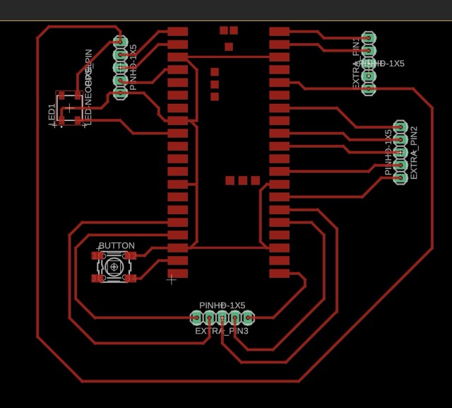 Next, in order to make sure that the board would mill and connect well, I made sure to avoid harsh angles in my traces and to connect to pins in straightforward ways. For doing this, it was helpful to go back and forth a bit with the bantam tools interface, to see where things were too narrow:
 In the end, I was able to configure the board so that it could be milled entirely by the big toolhead, avoiding the need to switch them in the middle of the job. Here is the final board design, including the board edge polygon:
 Fusion also gave me a convenient CAM preview of it:
 I submitted this to the bantam tool as a Gerber file because it wasn't reading my .brd correctly. For those confused by this in the future: make sure that you bring in the file and visualize the TOP of the board, so that you can see all of your components before printing!!
 Here is the finished product:
 Next, it was time to attach components. I laid out a set of pins, a button, and my Pico W microcontroller on the board to show where they would go. Unfortunately I was never able to locate a neopixel LED of the right size for the pads I had cut, but it wasn't an issue at this stage because the Pico has a built-in LED.
 To start, I only soldered on the Pico and the button.
 And I loaded Neil's hello.button-blink.RP2040 sketch into my Arduino IDE and uploaded this to the Pico. To my enthusiastic surprise, this worked on the first try!
With this working PCB in hand, I was prepared to continue adding components and further testing, which can be found in my Week 8 documentation.
And I loaded Neil's hello.button-blink.RP2040 sketch into my Arduino IDE and uploaded this to the Pico. To my enthusiastic surprise, this worked on the first try!
With this working PCB in hand, I was prepared to continue adding components and further testing, which can be found in my Week 8 documentation.