This week, we are connecting input and output on a single PCB. Since my final project does not plan to include any actuation components (motors, lights, speakers) and will instead either send its output to an endpoint via WiFi or simply write to its own memory to be dumped later, I stuck with an OLED display rather than introducing one of these new components.
I have used the multimeter and the oscilloscope in Week 8 and Week 5, but sensing power directly with a joulescope is a new effort. Please find documentation of the EECS group assignment for this week here.
Adding an Output Device to the PCB
Before I could add an OLED to my PCB, I had to fix a wire to my GPS module that had come apart from the solder. This issue, recurring from Week 3, signaled to me that the work this week would comprise not only adding my display but strengthening the board overall.
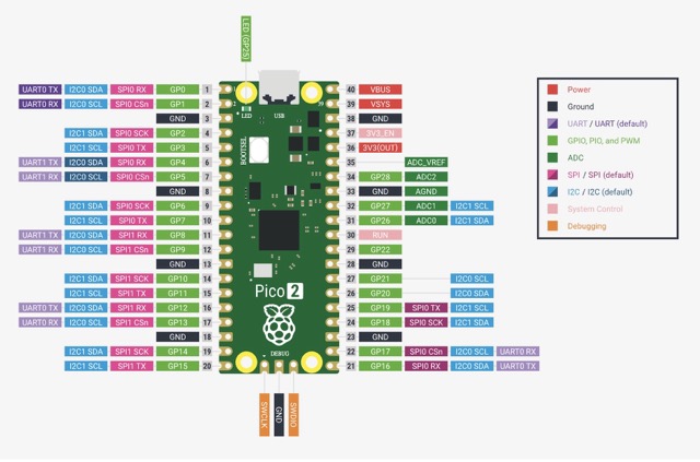
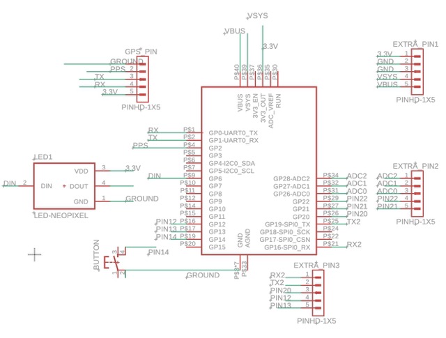
As I set about this work, I found it important to have my Pico W pinout, PCB schematic, and PCB print visualization handy so that I could remember which pin corresponded to which function. Here they are (for my own future convenience also):
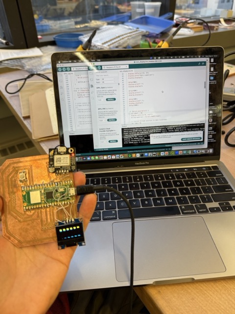
I decided to attach my new OLED to the position demarcated by "Extra Pin 1" in the printed visualization above, which I thoroughly ruined last week. I decided to make the best of this mistake by scratching away all signs of copper and solder paste with tweezers and using these holes purely as a structural element to hold the OLED which I then attached with wires.
The mini OLED display that had pins labeled GND (ground), VCC (input voltage), SCL (first I2C channel), and SDA (second I2C channel). These corresponded to pins 38, 37, 7, and 6 on the Pico W respectively. I am developing a reliance (or stylistic preferance?) towards attaching elements with wires I can see and adjust rather than to the pre-milled PCB tracks, and I did this more efficiently than last time.
In order to make sure both elements were functioning adequately, I ran two previous sketches on the board. First, I checked that my OLED was functioning by uploading my i-ching sketch from Week 3. This functioned fine, though I did notice this display has two regions of visualization-- a yellow strip at the top and a blue one below:
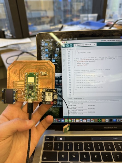
Seeing that the display worked, I tested the GPS again to make sure things were still in order, by loading my button pressing sketch. I had added to this some button outputs corresponding to writing data to flash memory, explained more under my Final Project.
While the button-triggered output shows GPS data to be invalid, I consider this a successful test because the microcontroller is receiving feedback from the GPS even though the GPS antenna isn't receiving anything inside the EECS lab.
Protecting the PCB
By this time I am thoroughly tired of breaking components on my PCBs through human error, structural deficiencies, and improper transport. While I am working on the human error part as we go, the latter two problems are easier to fix.
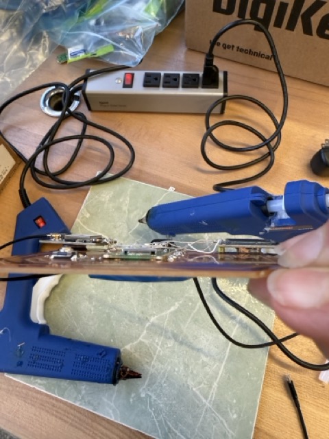
I improved the structural integrity of my board by adding hot glue bubbles underneath the GPS and display modules. These help the components to stay put since the electrical connections only attach them to the board by one side, and "structural soldering" is demonstrably a bad situation.
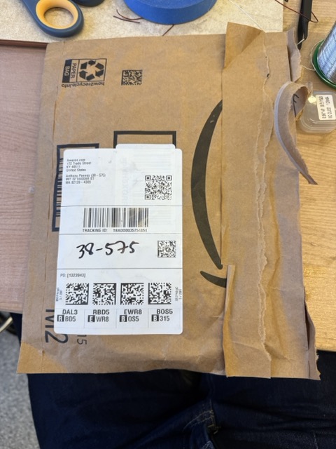
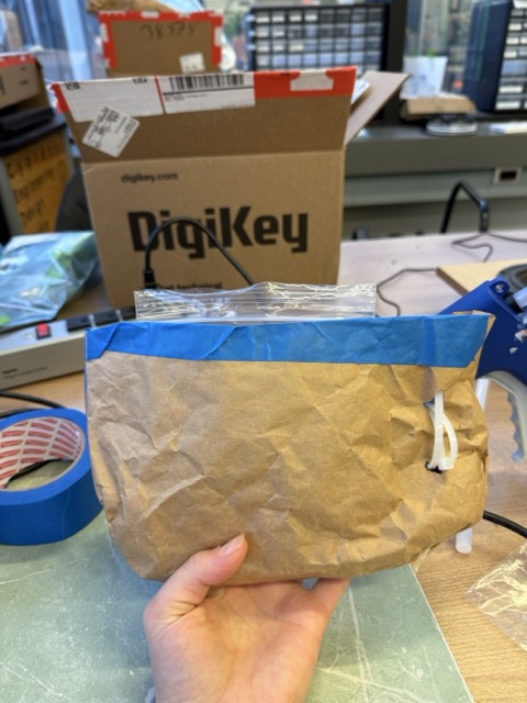
In order to improve my odds of transporting the board between home and school without breaking it, I decided to build a transport case with salvaged materials from around the lab. I started with an Amazon bubble mailer:
This I turned inside-out, lined with bubble-wrap, and fixed for closure with the top portion of a plastic bag:
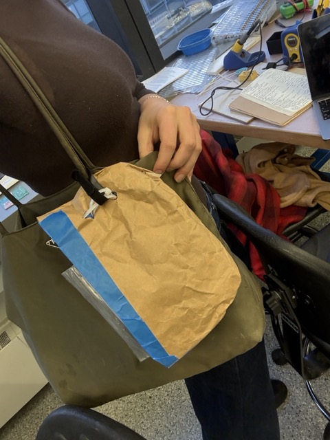
The PCB fit snugly. Here is the outside of the bag, which I added a zip-tie to in order to compress the interior area and give a loop for hanging:
Finally, I found a small strip of vel-cro that enabled me to connect the loop of the zip-tie to the strap of my school bag. With this, I have a very well-protected PCB pouch that will not get smushed by the other posessions in my bag nor, god forbid, toted to school loose in my car or pocket:
A triumph for upcycling and hopefully PCB safety, if not fashion!
Programming Output
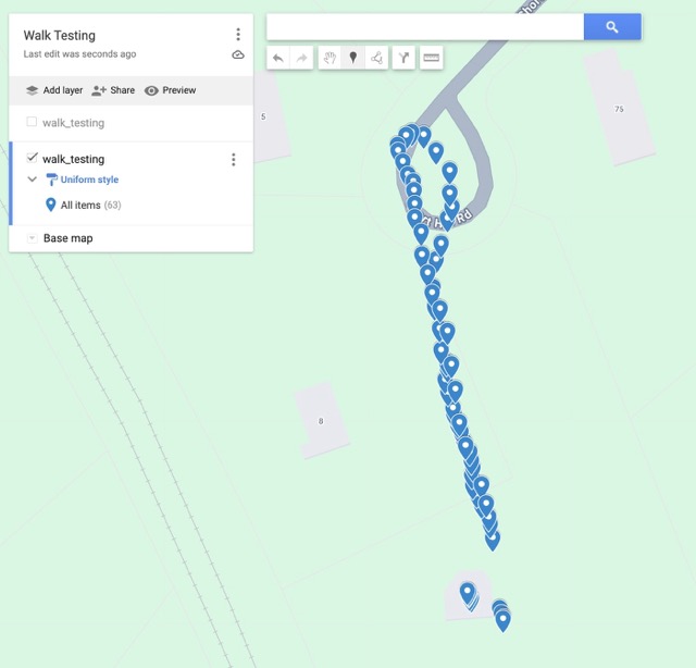
While I had hoped to make a device that would draw the shape of a path on the display, I felt that my display was too small this week to achieve something like this. I did test that strategy by dumping my GPS output to a CSV and reading that out to the Serial Monitor, then plotting it in Google Maps:
This demonstrates that the GPS does take fairly high-precision measurements. This walk applied GPS button measurements every ~5 steps, which is about the cadence of a walking stick contacting the ground (depending on the size of the stick). When I tie these measurements to the stick operation, I may need to downsample them, but let's see.
Another thing that I learned by taking this first walk was that my project will involve a lot of excursions outside, where it is getting colder every day. Given this factor as well as those above, for my assignment output I simply read out my GPS coordinates to the display:
This system now takes in data from the GPS, writes that to flash memory, prints it to the display, and can ultimately read it out as a CSV for plotting in Google Maps. An encouraging electronics step towards the final project!
Trials and Tribulations
Following are some observations of the process this week, and some challenges or disappointments to record:
I broke my PCB again in transit, hoping that my little pouch design will avert this in the future.
I still have to carry my entire laptop around in order to capture GPS data, because the laptop is powering the device. We have been advised against batteries in general, and I will need some feedback about how to power my walking stick for the fianl project version..
Learnings and Progress
Below is the delta between where I started on the skills for this week and where I arrived:
This week I finally started to feel confident running my Arduino code-- not sure why it took me so long to get this right (maybe because it messes up my monitor every time I have to plug and unplug the PCB from my computer?) but in any case, here are the actual steps. I am not sure why this was never obvious in any of the resources I looked at: (1) holding BOOTSEL, plug the data/power cable of the PCB into the computer, (2) select "UF2 Board" as the "board" under "tools" in the Arduino IDE, (3) upload the sketch (4) SWITCH the "board" under "tools" to the one with "usbmodem1101" in the name. Now you can view output on the Serial Monitor or upload new code and debug as needed.
The other key thing I learned is that I cannot copy infinite Serial Monitor content using Ctrl+C / Ctrl+V; rather, it only allows copying of information that is visible in the scrolling IDE window. This is a problem for accessing more than ~25 GPS coordinates at a time using the method I developed this week.
Resources and Acknowledgments
This week I had some actually useful conversations with ChatGPT, which are recorded here. Most of the useful content dealt with writing data to the Pi Pico's flash memory, for which I struggled to find any straightforward examples online-- while this task was primarily final project-focused, I also discussed PCB questions there for this week's assignment.
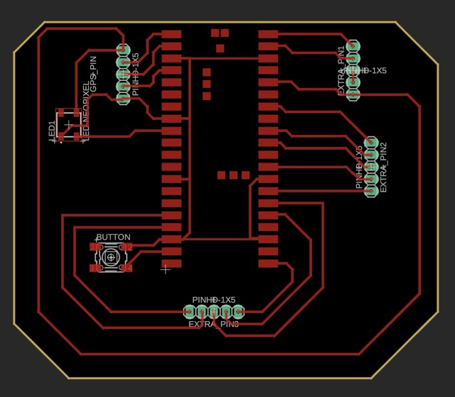 I decided to attach my new OLED to the position demarcated by "Extra Pin 1" in the printed visualization above, which I thoroughly ruined last week. I decided to make the best of this mistake by scratching away all signs of copper and solder paste with tweezers and using these holes purely as a structural element to hold the OLED which I then attached with wires.
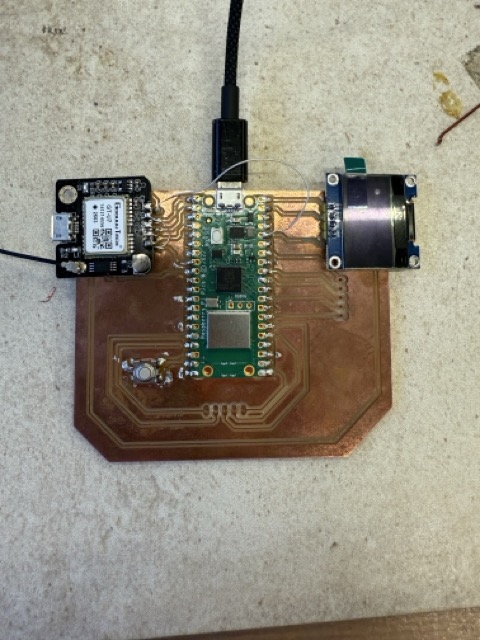 The mini OLED display that had pins labeled GND (ground), VCC (input voltage), SCL (first I2C channel), and SDA (second I2C channel). These corresponded to pins 38, 37, 7, and 6 on the Pico W respectively. I am developing a reliance (or stylistic preferance?) towards attaching elements with wires I can see and adjust rather than to the pre-milled PCB tracks, and I did this more efficiently than last time.
 Seeing that the display worked, I tested the GPS again to make sure things were still in order, by loading my button pressing sketch. I had added to this some button outputs corresponding to writing data to flash memory, explained more under my Final Project.
 While the button-triggered output shows GPS data to be invalid, I consider this a successful test because the microcontroller is receiving feedback from the GPS even though the GPS antenna isn't receiving anything inside the EECS lab.
 In order to improve my odds of transporting the board between home and school without breaking it, I decided to build a transport case with salvaged materials from around the lab. I started with an Amazon bubble mailer:
 This I turned inside-out, lined with bubble-wrap, and fixed for closure with the top portion of a plastic bag:
 The PCB fit snugly. Here is the outside of the bag, which I added a zip-tie to in order to compress the interior area and give a loop for hanging:
 Finally, I found a small strip of vel-cro that enabled me to connect the loop of the zip-tie to the strap of my school bag. With this, I have a very well-protected PCB pouch that will not get smushed by the other posessions in my bag nor, god forbid, toted to school loose in my car or pocket:
 A triumph for upcycling and hopefully PCB safety, if not fashion!
 This demonstrates that the GPS does take fairly high-precision measurements. This walk applied GPS button measurements every ~5 steps, which is about the cadence of a walking stick contacting the ground (depending on the size of the stick). When I tie these measurements to the stick operation, I may need to downsample them, but let's see.