Ben Z. Yuan - How to Make Almost Anything
Week 11: Input Devices
This week
Capacitive touch!
Assignment: add a sensor to a self-designed board and read it
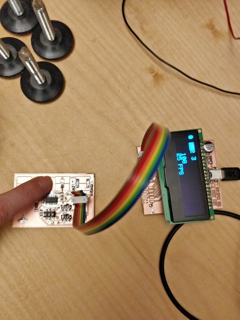
For this week’s assignment I decided to experiment with capacitive touch. As a basis, I used the overall circuit design suggested by Neil’s transmit-receive step response example from the input devices page. I made some modifications:
- Integrated four different pad patterns directly on the board for testing. One pattern consists of two rectangular pads, another consists of interleaving pads, and two others attempt to integrate indicator LEDs into the pattern.
- Connect power and communication through the 6-pin I2C header dictated by the final project output board.


While milling the board I decided (for no particular reason other than ‘it was there’ and ‘Bantam Tools apparently recommends this’) to try using a 80-degree engraving bit instead of the normal 1/64” flat endmill. This turned out to be a questionable decision: dialing in the correct cut depth ended up being something of a “trial and error” process, and I had several iterations where the bit was cutting too deep (which is catastrophic as cut width depends on cut depth directly).
Eventually I was able to mill a board where both the front side and back side had acceptable traces. The back side wasn’t perfectly dialed in but the board was still fine electrically.


The cut width on the front side was small enough that it started causing some problems as I tried to stuff and test the board:
- Tiny copper whiskers causing bridging between traces.
- Small spacing makes solder bridges very easy to form. Using extremely fine solder and carefully controlling feed rate helps.
Theory and practice of capacitive touch
The idea is this: software sends a voltage pulse on the sense pin and measures the size of the return pulse on the return pin.
I modified Atmel’s I2C peripheral example code to do the following on each loop:
- Assert +5 on the currently active sense pin.
- Measure the return voltage on the return pin after a small delay, using the onboard ADC.
- Assert GND on the currently active sense pin.
- Measure the return voltage on the return pin after a small delay.
- Store the difference in voltage in a buffer.
- Advance the sense pin counter by 1 increment (so do a different sense pin next loop).
During the process of debugging this board I discovered the following things:
- Boards must never be allowed to touch. (This makes voltage regulators emit copious amounts of magic smoke. Conveniently, this is an excuse for me to revise my final project board.)
- Magnet wire as a trace repair solution is fairly fragile. (Another excuse to revise my final project board.)
- The way Atmel’s example code works with the t44a’s USI peripheral and interacts with the Arduino Wire library (as used on my final project board) seems to preclude doing large amounts of processing between I2C read/write cycles. (In particular, if the t44a spends too long between reads from the I2C buffer, communication between the two boards grinds to a halt for reasons I haven’t been able to adequately characterize.)
- Whether or not the ADC is active and reading a channel is independent of whether or not the corresponding pin is actually set as output! It is valid to set the ADC to read an output pin – even though there are not really any good reasons to do this.
But eventually I was able to get an adequate capacitive response from the 4 pads.
Because of the small size of the pads the integrated LEDs end up getting in the way of making a clean touch, so it is probably easier to leave them out. The interleaved pads are able to produce a response over a slightly larger region of potential touches (determined empirically) than the non-interleaved pads, so any replacement for the Adafruit Trellis probably wants to use them.