Ben Z. Yuan - How to Make Almost Anything
Week 3: Electronics Production
This week
We mill PCBs and solder surface-mount boards, making a microcontroller programmer.
PCB milling
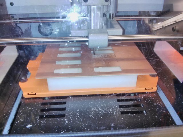
The EDS shop has access to a Roland SRM-20 tabletop CNC milling machine. This device provides precise cutting within an 8” x 6” x 2.38” volume. This week, we use it to cut out PCB traces and boards from a copper-coated resin stock, first milling away copper to produce traces, and then cutting out the board outline.
Mechanical milling has the advantage of not requiring noxious or corrosive chemicals (unlike etching). However, this technique only works effectively for boards with only one (or maybe two) layers of traces. Because it is a mechanical process, there are also limits to the amount of spacing between traces that is permitted: in particular, gaps between traces cannot be smaller than the size of the milling bit (nominally 1/64” inch).
Group exercise: characterizing milling process design rules
We characterized the limitations of our milling process; akaspar describes this process in full detail.
The takeaway is that traces can be extremely fine (down to .001” / 0.02 mm) but gaps between traces are necessarily limited by the endmill width (1/64” / 0.397 mm).
Individual exercise: milling a PCB
At the course runners’ suggestion I decided to replicate the FabTinyISP Minimal initially designed by Brian Mayton. The CBA Mods toolchain has a preset pipeline for converting PCB designs in PNG format (separate trace and outline files) into toolpaths for the SRM-20 milling machine. Conveniently, the FabTinyISP Minimal description page includes the PNGs necessary to replicate the design – and, since everyone else appears to be producing more-or-less the same design, the PNGs were already loaded onto the control computer.
I loaded the trace PNG and generated a toolpath with an offset of 5, then found an appropriate origin on an uncut piece of board. (+y is toward the back of the machine, +x is toward the right). The origin is at the lower left corner of the design PNG file.
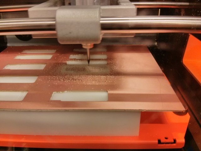
One problem that can arise when milling traces is, because the nominal cut depth is so small (only 0.004”), the tiniest incline in the board stock can cause the traces to fail to mill properly over part of the board.
akaspar suggested re-milling after physically clamping the milling bit to the board with greater force while setting the set screw, which seemed to yield acceptable results.
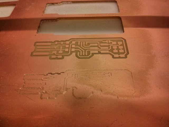
After milling the traces I loaded the outline PNG and generated an outline toolpath with an offset of 1, and loaded in the 1/32” milling bit, then had the machine mill out the board outline.
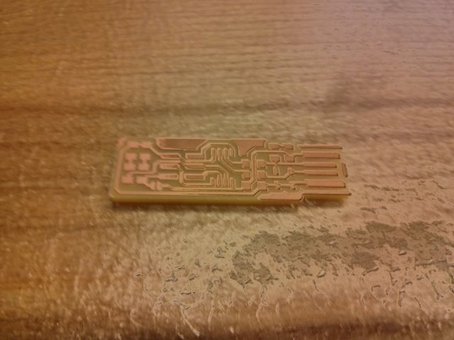
After this was done I had to use a prying tool to remove the cut-out board (as the stock was secured to a sacrificial plastic block with double-stick tape, and the board was laid out on top of a tape piece). The result was a very nice milled “printed” circuit board, ready for the next steps.
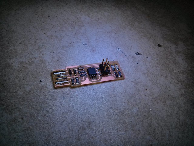
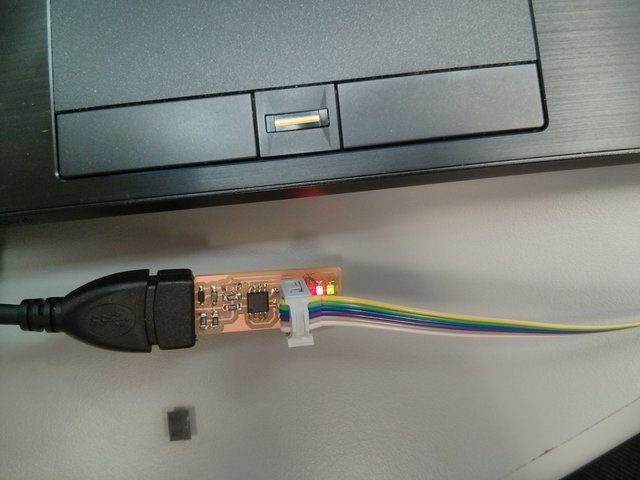
Individual exercise: assembling a programmer
Surface-mount parts are tiny.
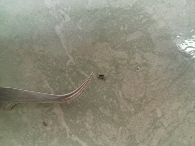
Populating the board was mostly an exercise in patience. I’ve done soldering before, and working with surface-mount components follows the same basic principles as through-hole soldering. However, one needs a good set of tweezers to manipulate the components while soldering – as the components are too small to move by hand while the soldering iron is live!
Most of the parts we’re using are 1206 size (0.12” x 0.06”) or in that size range. As SMT parts go these are actually relatively large - I wouldn’t want to be caught trying to do e.g. 0402 or smaller by hand!
One trick that gavindar mentioned to us, that I used with success, is to place a bit of solder on a target pad, and then placing the component while melting the solder to create a mechanical connection. This allows the other lead(s) of the component to be soldered properly without worrying about the part being displaced afterwards.
It’s fairly easy to add too much solder to a surface-mount joint, especially when using thicker solder wire. Thinner solder definitely helps with surface-mount work. If too much solder is applied to a joint then solder wick can be used to remove the excess – which I had to do a number of times before I had solder joints with which I was satisfied.
Eventually I ended up with a fully soldered board. On to programming!
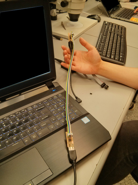
Individual exercise: programming a programmer
The solder thickness on the USB contacts had to be adjusted several times before I could get a solid connection with the provided USB extension cable, but eventually I was able to get a reliable contact. Following the instructions on Brian Mayton’s writeup I was able to get the programmer programmed successfully without hitches.
As a bonus test I built a 6-wire ribbon cable (with gavindar’s help) and, using it and my programmed board, programmed natalie’s board:
When both boards are connected the red LED happens:
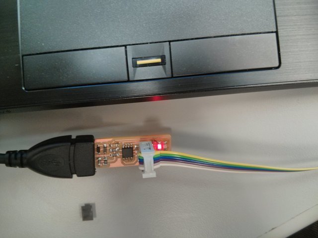
And during programming the green LED happens:
This was a successful week.