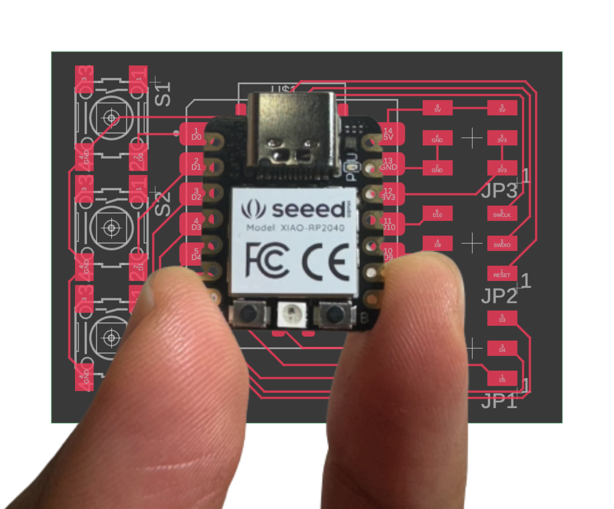
Electronics Design
"Electronic design automation (EDA), also referred to as electronic computer-aided design (ECAD), is a category of software tools for designing electronic systems such as integrated circuits and printed circuit boards." -Wikipedia
Group Assignment
1. I worked with my group to use an oscilloscope and a multimeter.
Working with a large group of students from the Architecture section, we explored the use of an oscilloscope (Fig. 1A). During this process we used a wave generator to establish a frequency that we could then visualize on the oscilloscope. We adjusted the amplitude of the wave and and noted the corresponding change.
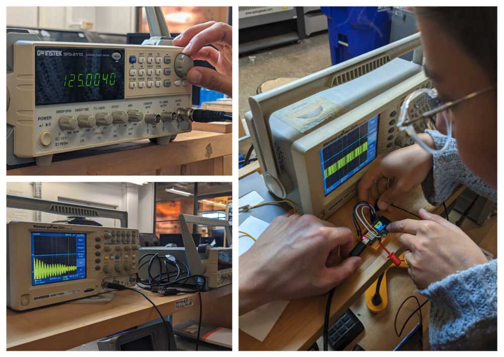
Fig. 1A. Using the oscilloscope.
We also tested the resistance of a resistor using a multimeter (Fig. 1B). We also used it to check the voltage of the multimeter itself, discovering that it operates with 5V.
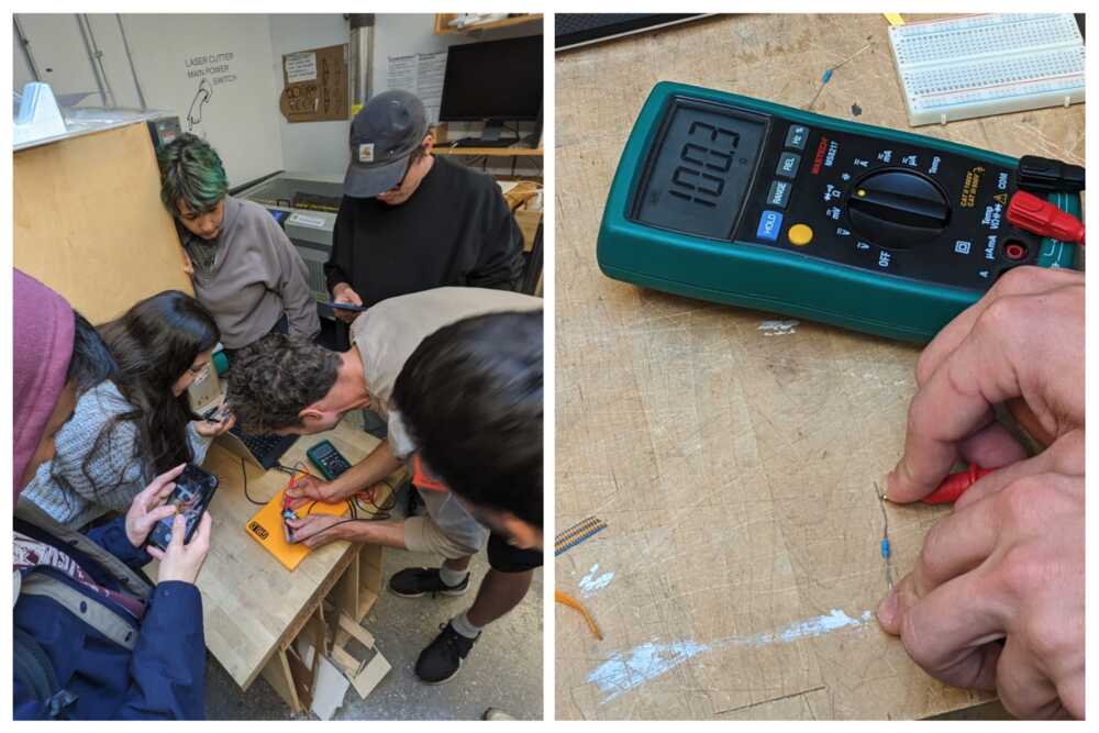
Fig. 1B. Using the multimeter.
There were a lot of students involved in the group assignment this week!
Individual Assignment
2. I designed a circuit board with three buttons.
Hoping to make progress toward my final project, I decided to design a circuit board with buttons that could later be programmed to operate the gut machine. Watching EDA tutorials, I familiarized myself with the electronics design capabilities of Fusion 360 and made the first iteration of the circuit diagram (Fig. 2A). In this design I added three swtiches and three connectors.
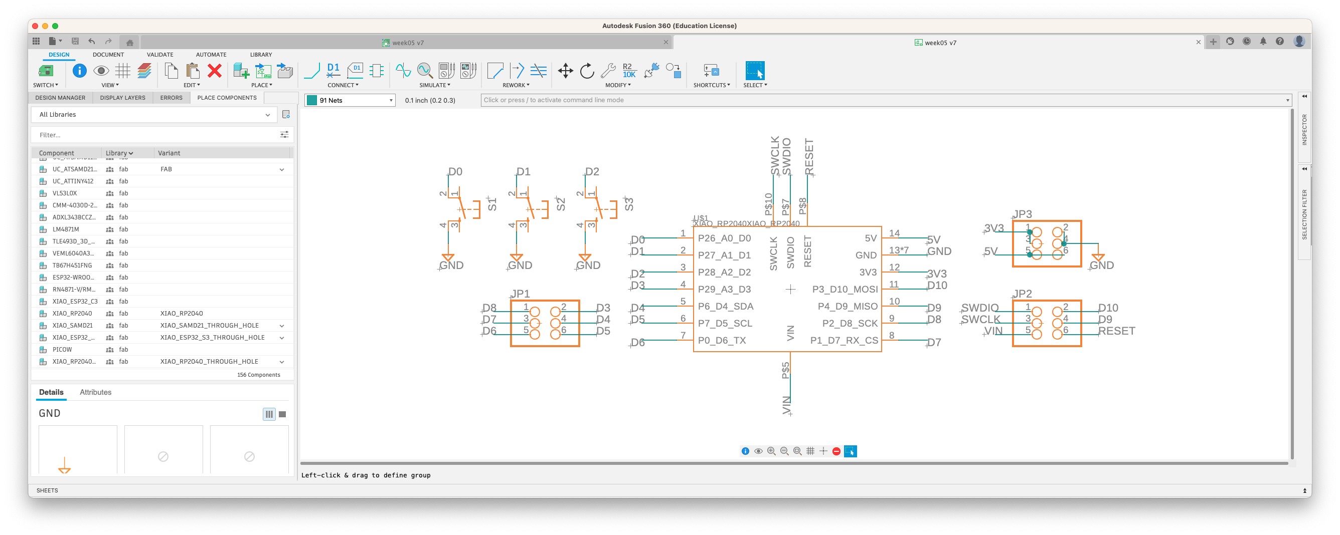
Fig. 2A. First iteration of the circuit diagram.
When I was happy with the circuit diagram, I switched over to the PCB layout (Fig. 2B). I started routing with the switches (S1, S2, and S3), which went fine. However, when I started routing with the connectors (JP1, JP2, and JP3), I realized I had to make changes to the circuit diagram. Specifically, I noticed that for the JP2 connector I would not be able to route to desired pins without crossing over other routes.
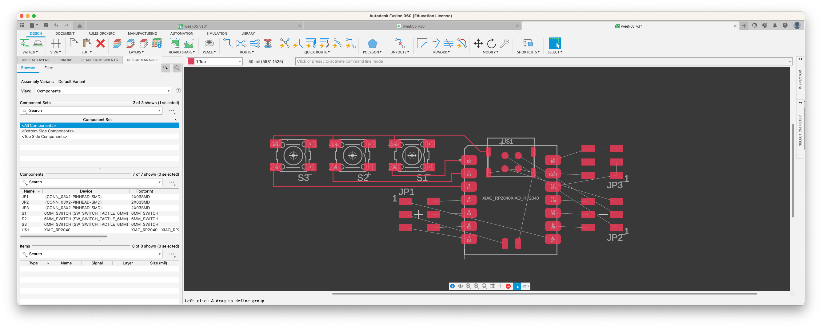
Fig. 2B. First iteration of the PCB layout.
Noticing my error above, I went back to the circuit diagram to make changes. In fact, this was quite an iterative process, as I ended up having to make changes at least 5 times before reaching the final circuit diagram (Fig. 2C).
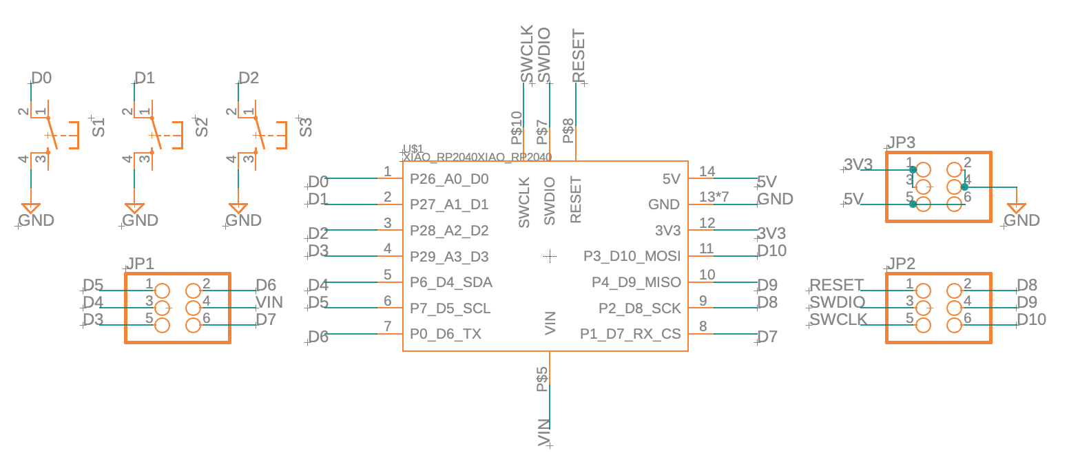
Fig. 2C. Final iteration of the circuit diagram.
In the final iteration of the PCB layout the remaining routes were able to be made without crossing any existing routes (Fig. 2D). I even made some design changes including reorganizing the location of the switches and making the PCB layout as compact as possible. The Fusion 360 file can be downloaded here.
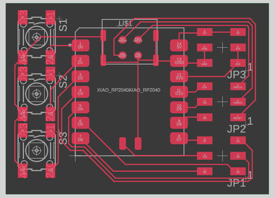
Fig. 2D. Final iteration of the PCB layout.
I experience a little difficulty attempting to export the layout as an image that could then be uploaded to the PCB machine. I discovered an online message board that pointed me in the right direction (Fig. 2E).
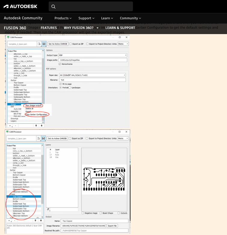
Fig. 2E. CAM Processor tool in Fusion 360 for exporting images.
With the help of the CAM Processor tool, I was able to export a high quality .jpg image of my PCB layout (Fig. 2F)!
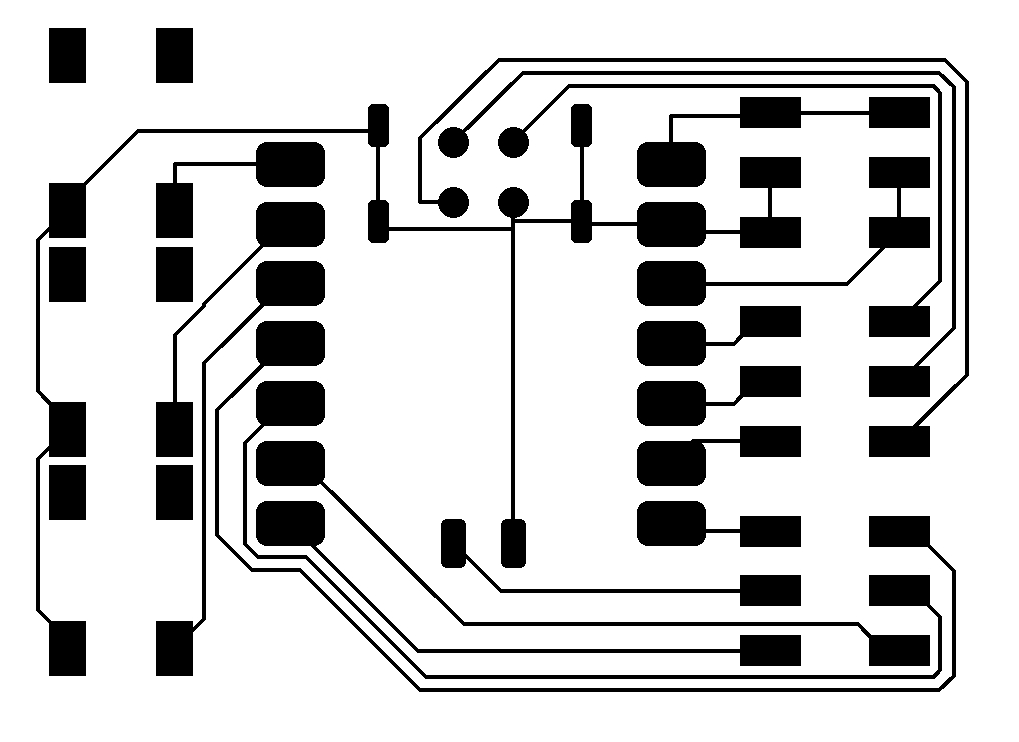
Fig. 2F. Image of PCB layout.
I am looking forward to physically making my printed circuit board in a future week!