Week 6: Electronic Production
This week we worked on milling our own PCB designs. We use the OtherMill to mill the copper boards and use bantam tools to process the brd files into gerber files.
I made a few PCB designs this week. I ended up milling something that can sense light and display something using that on a display. I use a Phototransistor to do this. phototransistors are simpler than photodiodes for this, with no separate amplification needed, and the RP2040's ADC can read them directly. I initially considered an LDR but phototransistors have way better temporal response, as well as is much larger. It works like a regular transistor but is activated by light and typically has three terminals: the collector, base, and emitter. When light hits the phototransistor, it allows current to flow from collector to emitter.
Here is the schematic. This uses pull-up resistors for the display for the SLC and SDA ports. I also added a resistor to the phototransistor to limit the current going through it. Fusion 360 also gives you a bill of materials.
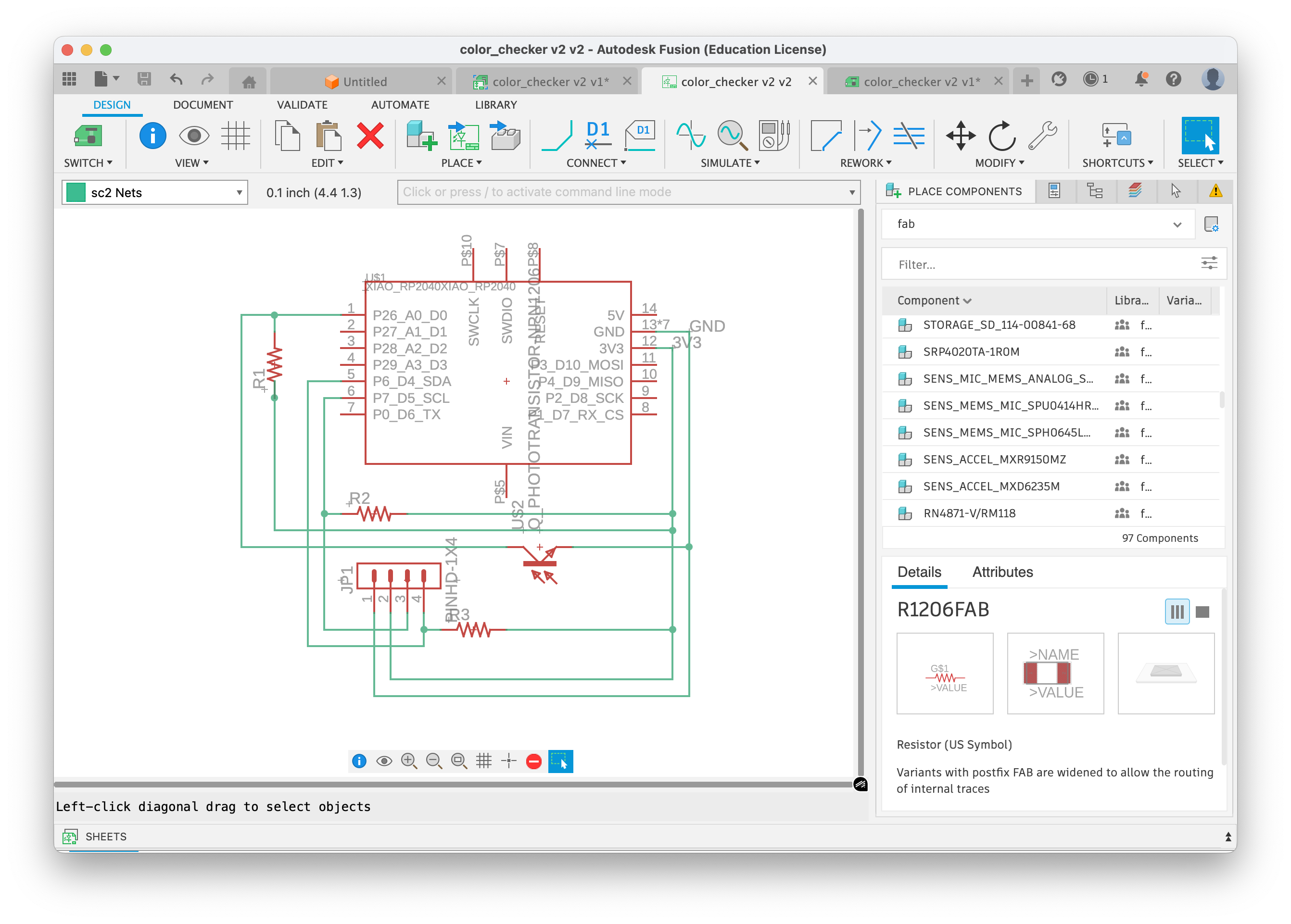
| Part | Value | Device | Footprint | Description |
|---|---|---|---|---|
| JP1 | PINHD-1X4 | PINHD-1X4 | 1X04 | Pin Header - 4 Position |
| R1 | — | R1206 | R1206 | Resistor |
| R2 | — | R1206FAB | R1206FAB | Resistor (FAB) |
| R3 | — | R1206FAB | R1206FAB | Resistor (FAB) |
| U$1 | XIAO RP2040 | XIAO_RP2040 | XIAO_RP2040 | XIAO RP2040 Microcontroller |
| U$2 | Phototransistor | Q_PHOTOTRANSISTOR-NPN1206 | OP1206 | NPN Phototransistor |
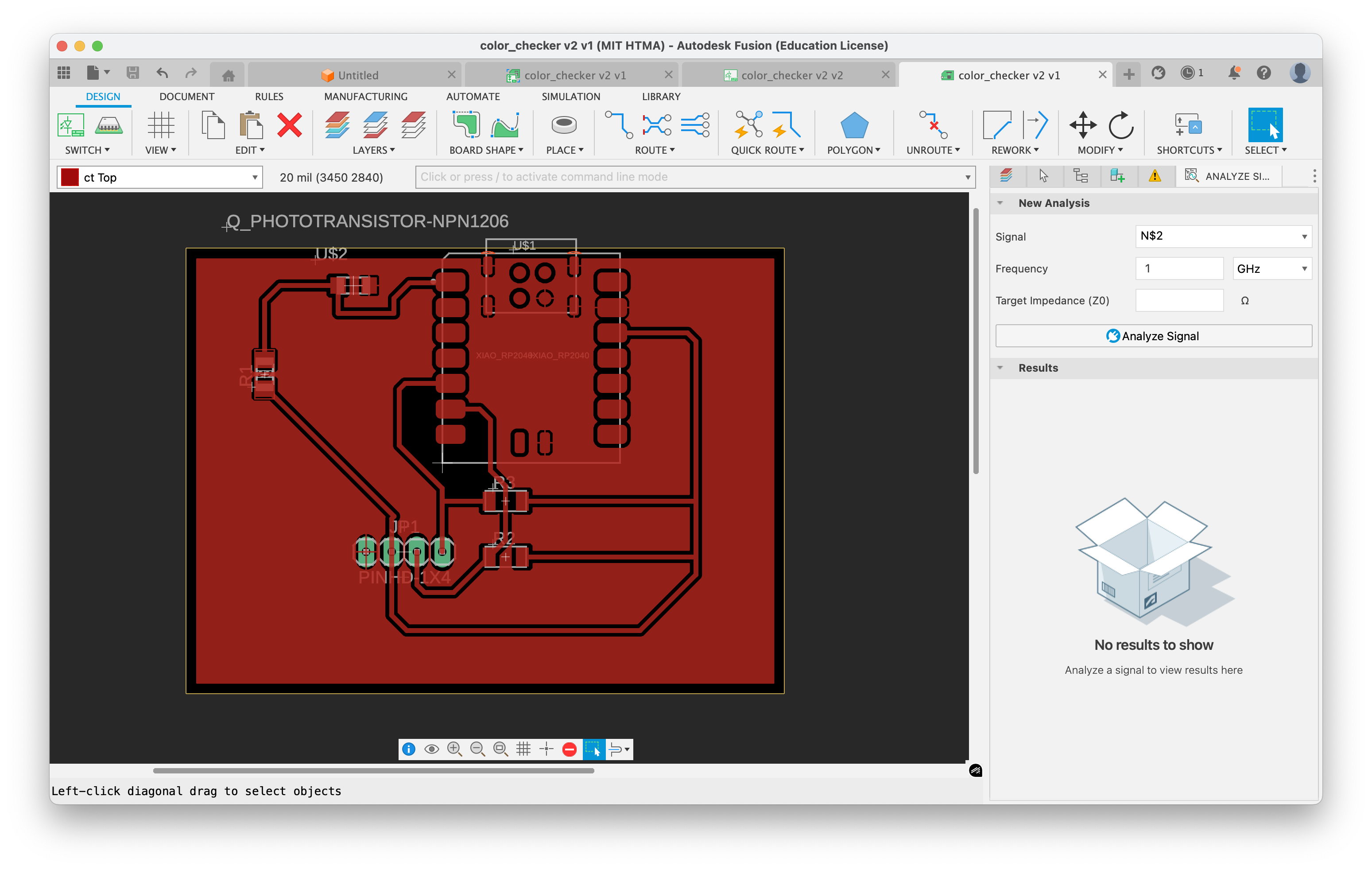
Here is the routing of the board. We set the design rules to 16 mil because of the size of our tools. Instead of routing ground, I used polygon pour to make it easier to connect to ground, and more importantly, it acts as a heat sink during soldering—the ground pins don't overheat as easily.
Then, I added it to the Bantam tools software:
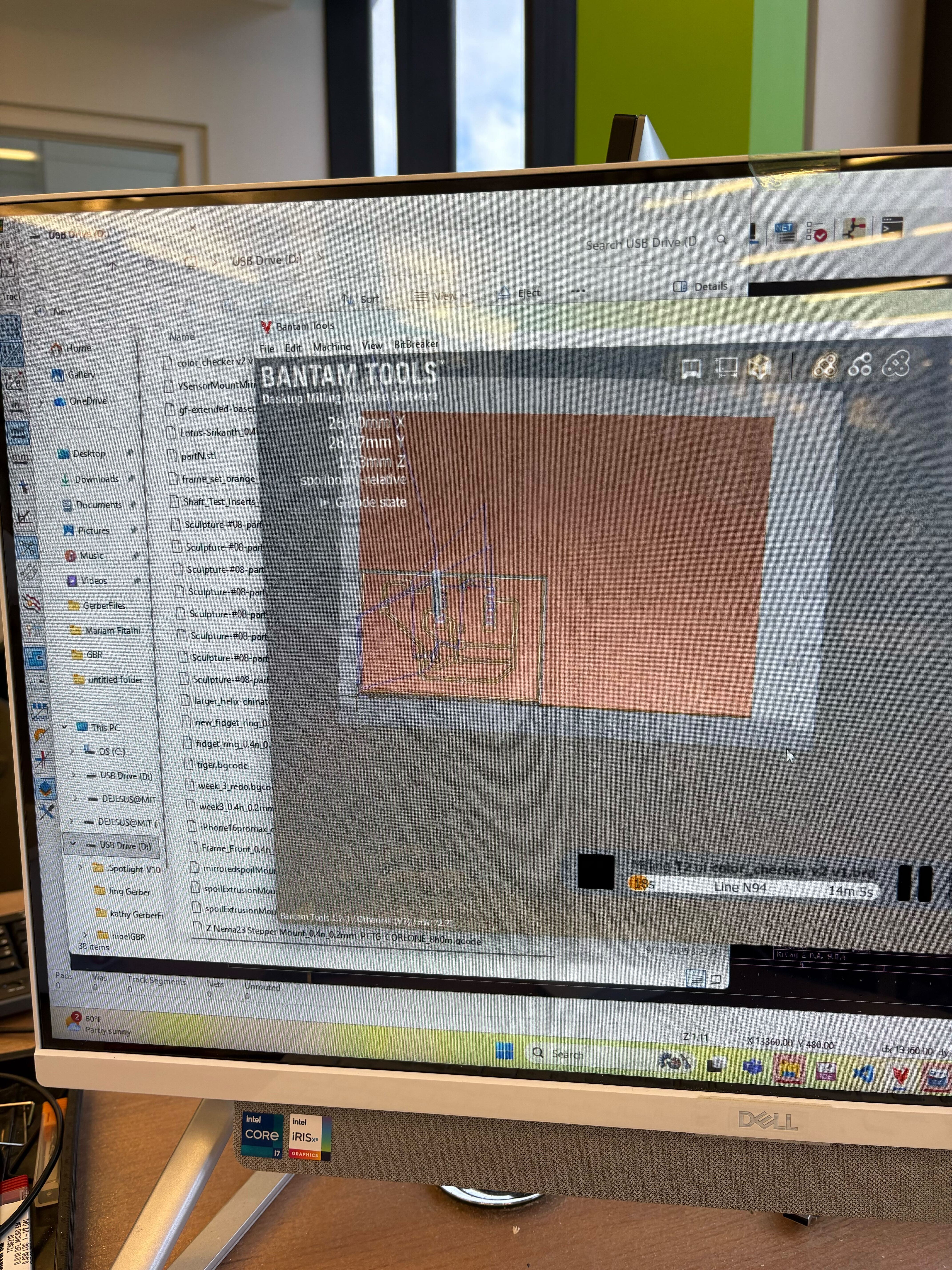
This requires 2 tools, because some of the footprint for the RP2040 board requires the 1/64 tool, and the rest just needs 1/32. There were a few changes I made to the board (using a FAB-version of the resistor) that reduced the need for 1/64 milling.
The final step was to solder the board together. I used 5k resistors for the pull-up resistors and a 5k resistor for the phototransistor. The pull-ups on i2c are 5k bc that's what the OLED spec sheet suggested for 3.3v operation.
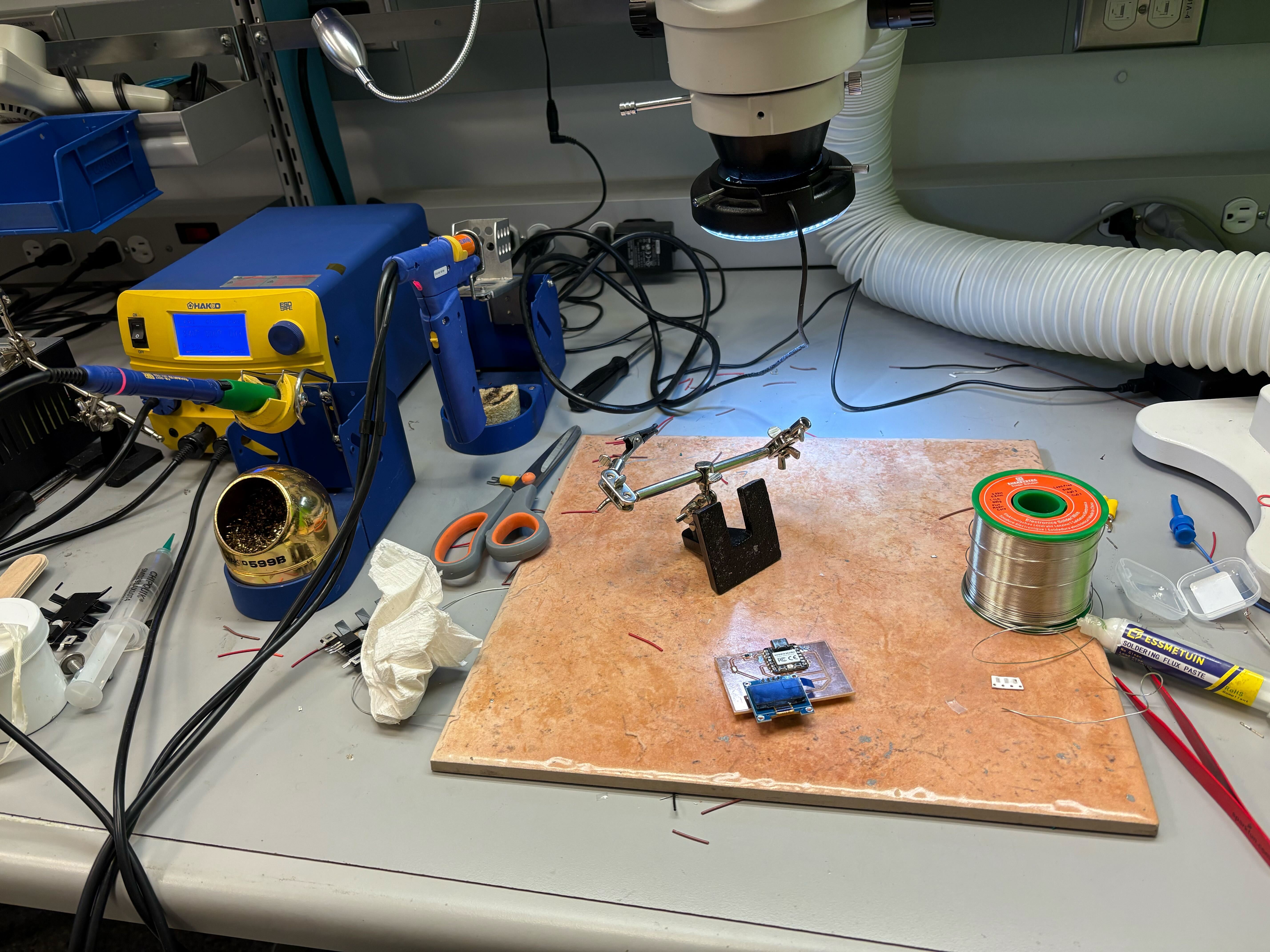
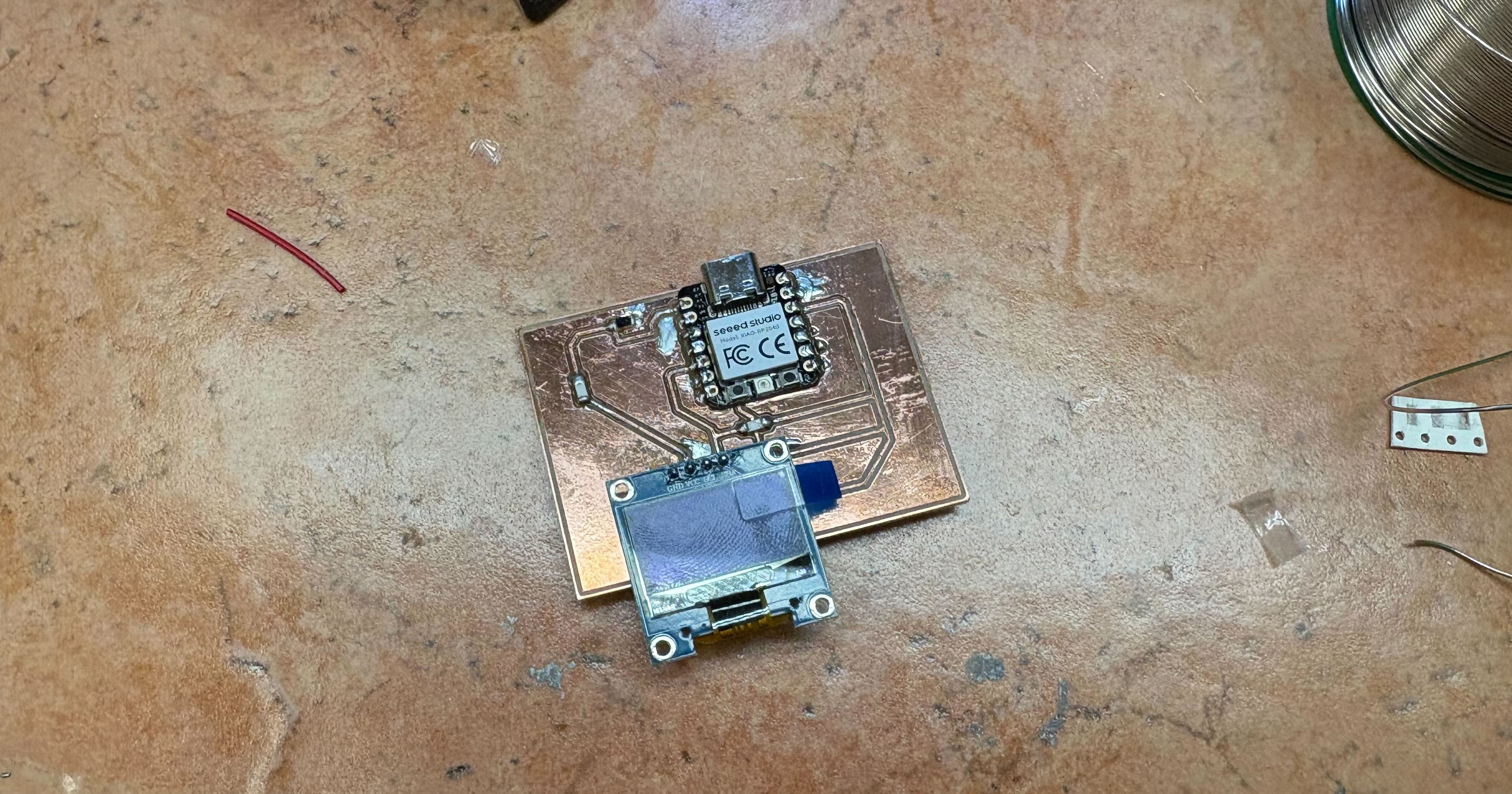
Final Product!
Todo: I need to upload the code to the board and test this. Here's the basic code I'm using to test this:
#include
#include
#include

#define SCREEN_WIDTH 128
#define SCREEN_HEIGHT 32
#define OLED_RESET -1

Adafruit_SSD1306 display(SCREEN_WIDTH, SCREEN_HEIGHT, &Wire, OLED_RESET);

const int PHOTO_PIN = A0;  // P26_A0_D0

void setup() {
	pinMode(PHOTO_PIN, INPUT);

	Wire.setSDA(6);  // P6_D4_SDA
	Wire.setSCL(7);  // P7_D5_SCL
	Wire.begin();

	if(!display.begin(SSD1306_SWITCHCAPVCC, 0x3C)) {
	while(1);
	}

	display.clearDisplay();
	display.setTextSize(1);
	display.setTextColor(SSD1306_WHITE);
	display.display();
}

void loop() {
	int raw = analogRead(PHOTO_PIN);
	int light = map(raw, 0, 1023, 0, 100);

	display.clearDisplay();

	display.setCursor(0, 0);
	display.print("Light: ");
	display.print(light);
	display.print("%");

	int barWidth = map(light, 0, 100, 0, SCREEN_WIDTH);
	display.fillRect(0, 16, barWidth, 8, SSD1306_WHITE);

	display.display();
	delay(100);
}
Thanks so much to Anthony for answering my many circuit design questions (so close to Wednesday too) and Eghosa for explaining some of the things I had missed when I was out of town and confused. :)