Electronics Production
This weeks project went way smoother than I had expected. I had done some milling at the GSD and had had some frustration with the mastercam UI. Here, Neil's Lecture actually prepared me very well for the basic procedure of milling the circuit board and even the techniques of soldering all the components. With the help of Rob, the Lab Tech, I completed my board in about an hour.
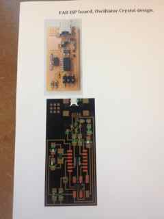
As I quickly learned, the fab modules are excellent tools and are very well calibrated for the needs of the class. We are given a simple image of the board as a png. The fab module automatically adjusts for tool path offsets and has cut depths pre-programmed in. The first thing we did was to tape down a scrificial board with the copper side down, so our final pass to cut the board out would not dig into the bed of the mill. We used double sided tape and covered as much of the board as possible without overlapping tape or wrikling it. Next we taped a smaller board, copper side up, in the bottom left corner fo the mill. The orientation on the computer screen is the same as in the mill, which makes it easy. Using the fab module, we adjusted x and y coordinates to the bottom left corner of our millstock. Then we use the technique Neil described to zero the z axis. This involves lowering the millhead almost to the bottom, and then loosening the bit to allow it to rest on the copper surface. We had to be careful to not drop the bit so it wouldn't crack. We used a 1/64in end mill bit, and the fab module worked like a charm, and soon we had the circuit cut out of the top surface of the plate.
 My board basically fills the entire piece of stock, but it should be noted that it was the third circuit board milled from one piece. After each board was cut out, we re-zeroed the bit and ran the file again. Next we used the 1/32in end mill to cut the board out from the rest of the stock.
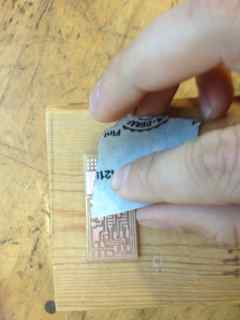 The first two boards did not cut out completely, and the remaining material had to be snapped off to remove the circuit, so I lowered the max depth in the fab module. It cut out the board fine, but had to take an extra pass around the board, and ended up cutting a channel in the sacrificial board below. before soldering I gave the board a light sanding to prep the surface.
 Rob had the brilliant idea of printing out a photo of the finished board and a schematic of the components. I laid double sided tape down on the schematic and placed the individual components there on the image. Then as I soldered, I just pulled individual components from the diagram and soldered them in place.
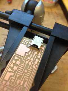
 I started with the USB header, since it had the super-fine leads that had to be wicked. I tacked it in place with a dab of solder, soldered it firmly in place in the corners, and then gobbed up the leads. The copper wick worked like a charm and cleaned the joints right up. Amazing!
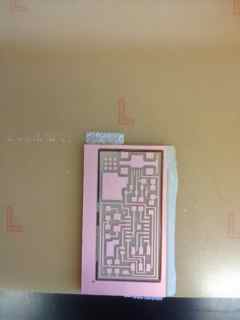
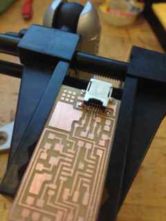
 Progress pics....
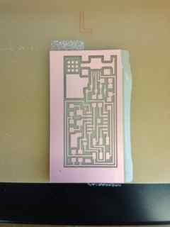
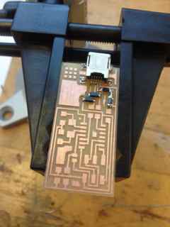
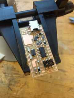
and the finished board!
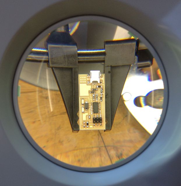
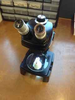 The microscope came in handy for identifying parts and orienting the diodes and IC. I also used it at the end to check my solder joints to make sue I didn't have any bridges that would short circuit.
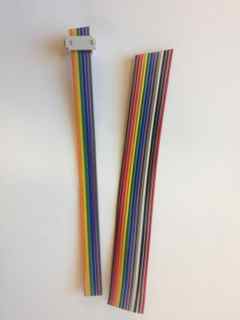
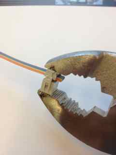 I used pliers to clamp the adapter onto the cable to fit on the 2x3 header.
Ad finally the finished board!
Right now, I am on an airplane to Slovenia for a Studio Trip, so I will have to test the circuit when I return in a week! Updates to come!