19 Oct 2016 · 4 min read
This week’s assignment was to make something big using a CNC. We had a single
piece of 4’ x 8’ x 7/16” oriented strand board (OSB) for us to use.
I decided to make something useful for my room. I do lots of outdoor
activities, each requiring different types of shoes. My shoes were taking up
too much floor space, so I decided to design a shoe rack. The first step was to
measure the shoes I had so I could figure out appropriate dimensions for the
shoe rack. I found that the largest shoes were around 12 inches long, 8 inches
wide for the pair, and under 10 inches tall.
Sketches
After getting this information, I started making sketches on a piece of paper.
I didn’t want to use wood glue or nails or screws, so I initially thought about
making a simple press-fit design. I wasn’t sure how well press-fit would work
with OSB without very high-precision cuts, so I decided to go with a different
design that uses a peg, held in place by gravity, at a 90-degree angle to the
joint:
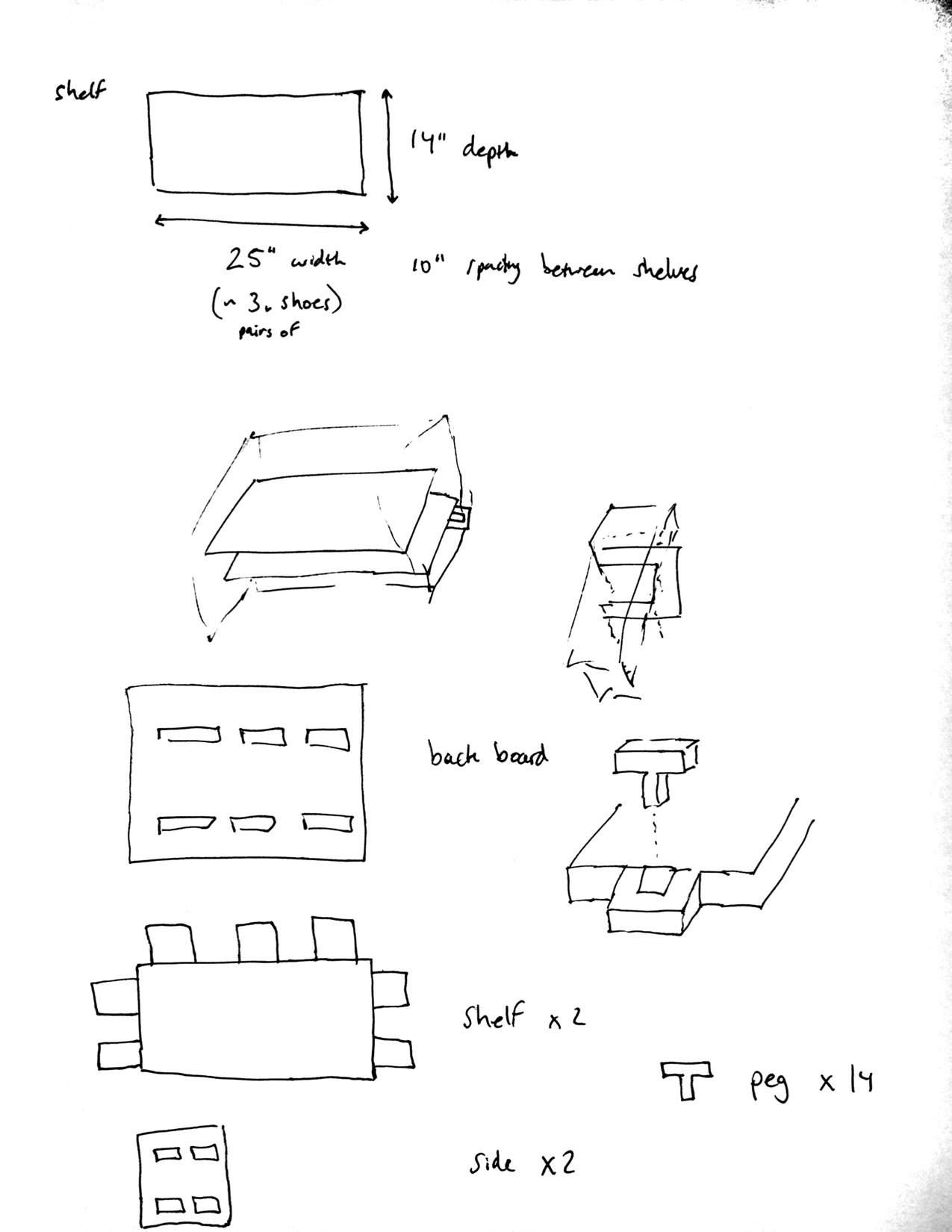
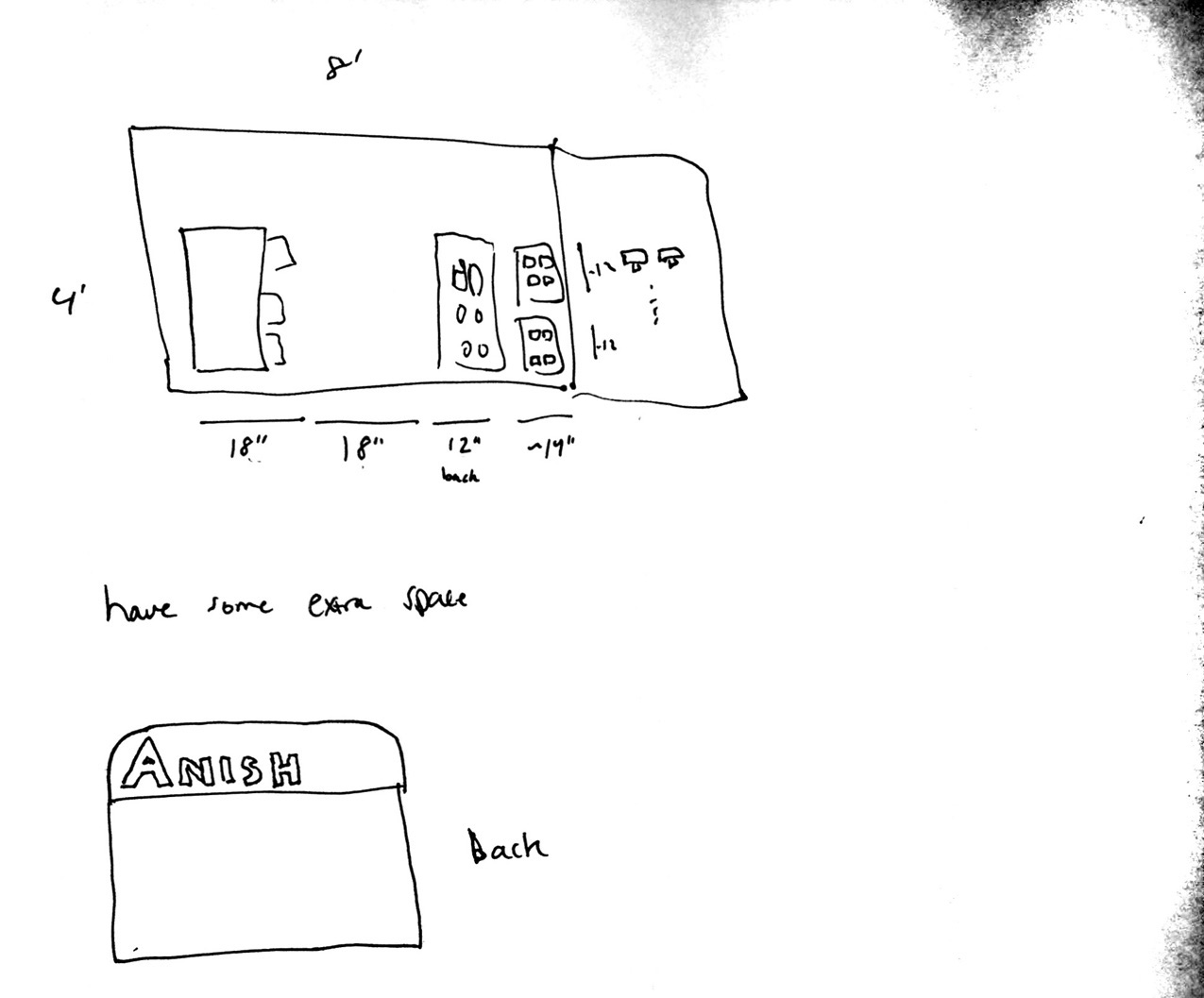
I made sure that everything would fit on my 4’ x 8’ OSB:
CAD
I decided to use Fusion 360 to design my shoe rack. I had used this software
only once before while designing my press-fit kit, so I was looking
forward to getting some more practice using the tool.
It took me about an hour and a half to complete a parametric design of the
part:
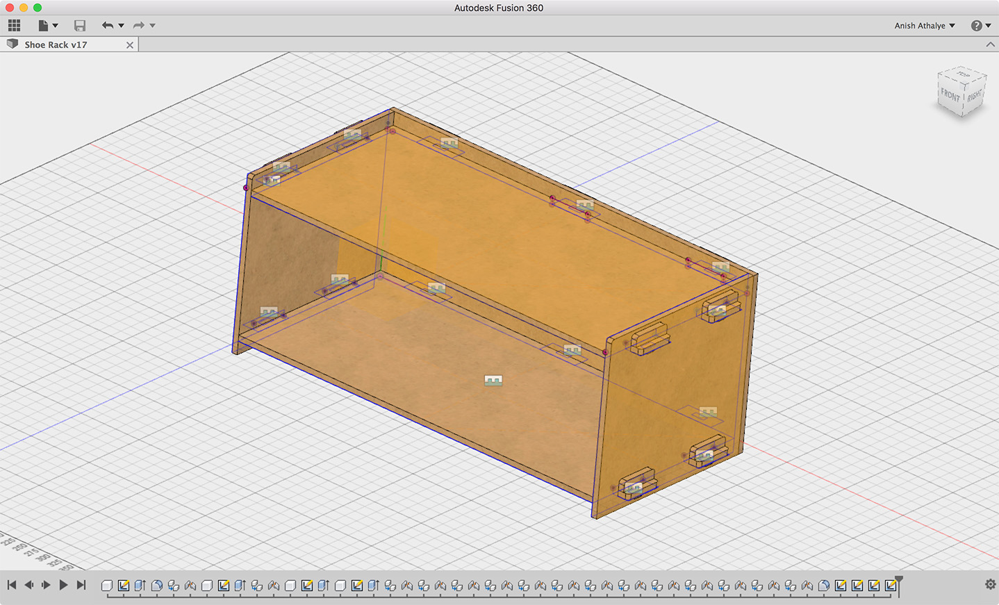
During the process of making the part, I made several mistakes that I had to go
back and fix. One of the bigger mistakes was caught when checking for
interference (overlapping volumes) — I found that my back panel was missing
some cutouts because I had not selected all the holes when extruding the part.
I fixed this using Fusion 360’s parametric timeline, which made the fix really
easy; going through this process also helped me better understand how the
parametric timeline works.
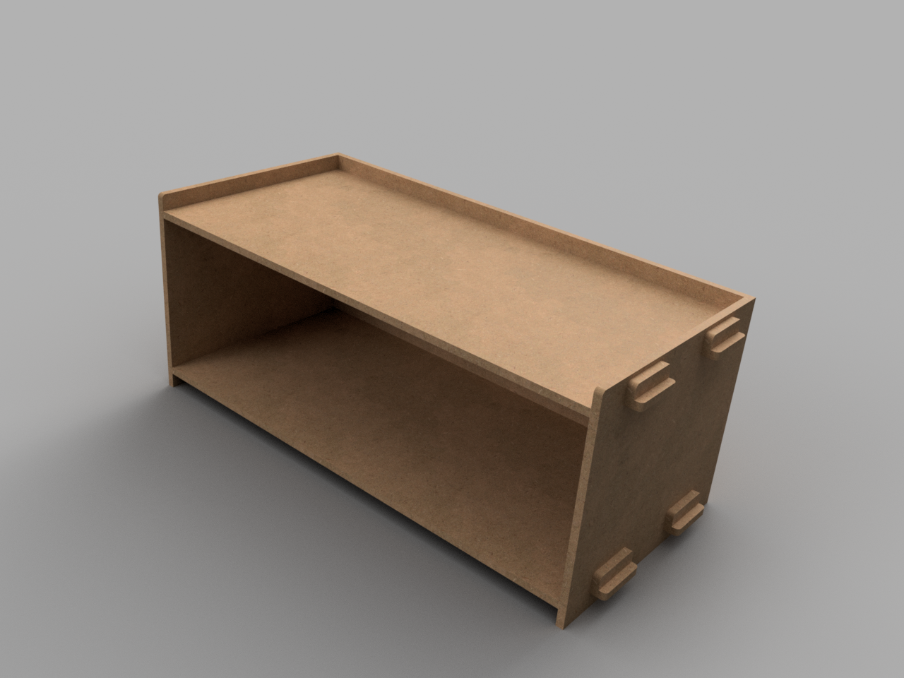
I decided to avoid engraving my name in the piece, because the inexpensive OSB
didn’t seem to work very well for engraving in tests done earlier.
After completing my design, I noticed that I had a little extra space available
on my piece of OSB, so I decided to change what I had in my sketches and change
the width of the shoe rack from 25” to 30”. Thanks to the fully parametric
design, this step took about 10 seconds.
Here’s a render of the final version of the shoe rack:
Machining
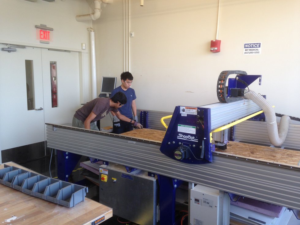
I used the ShopBot CNC router in the IDC to cut my piece. Here’s a picture of
me and Kevin
Kwok
loading the 4’ x 8’ piece into the machine:
Creating the toolpaths was very straightforward — I cut out the holes first,
and then I cut out the outlines. After creating the toolpaths, I zeroed the
machine and started my job. Here’s a picture of the job in progress:
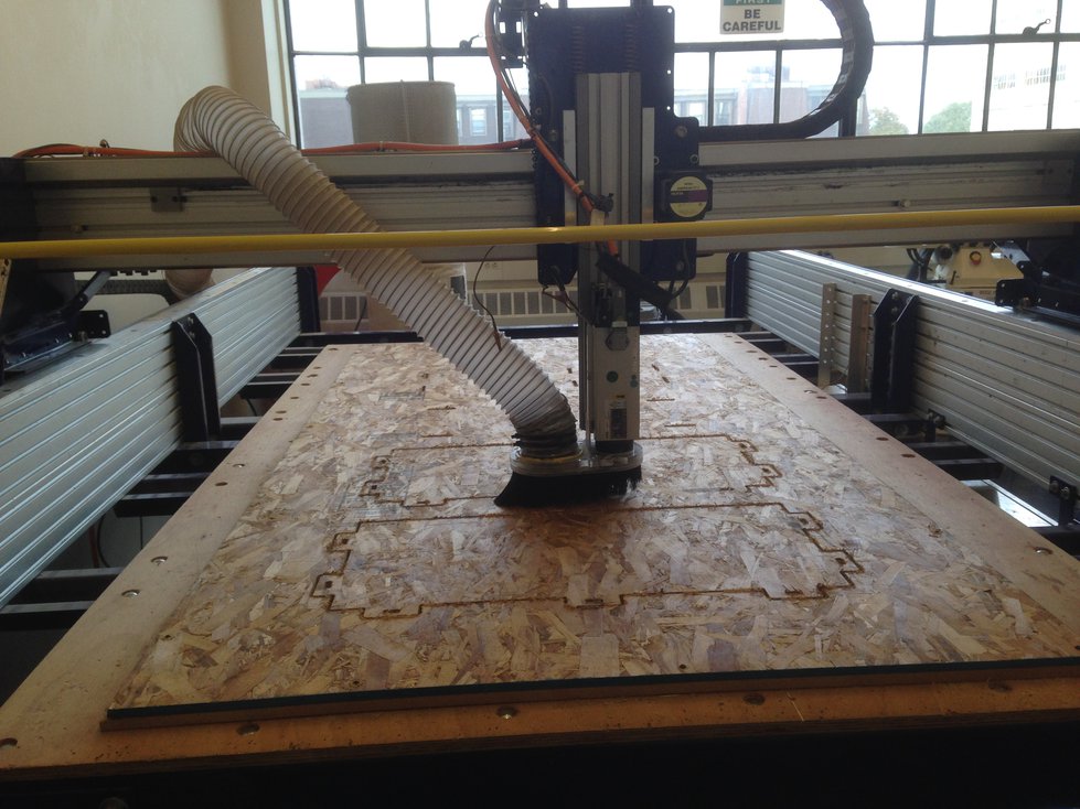
The entire job took about 21 minutes.
When cutting the small pegs, one of the pieces got sucked up by the vacuum
attached to the end effector! I realized that this was because there was only a
single tab connecting the piece to the rest of the board:
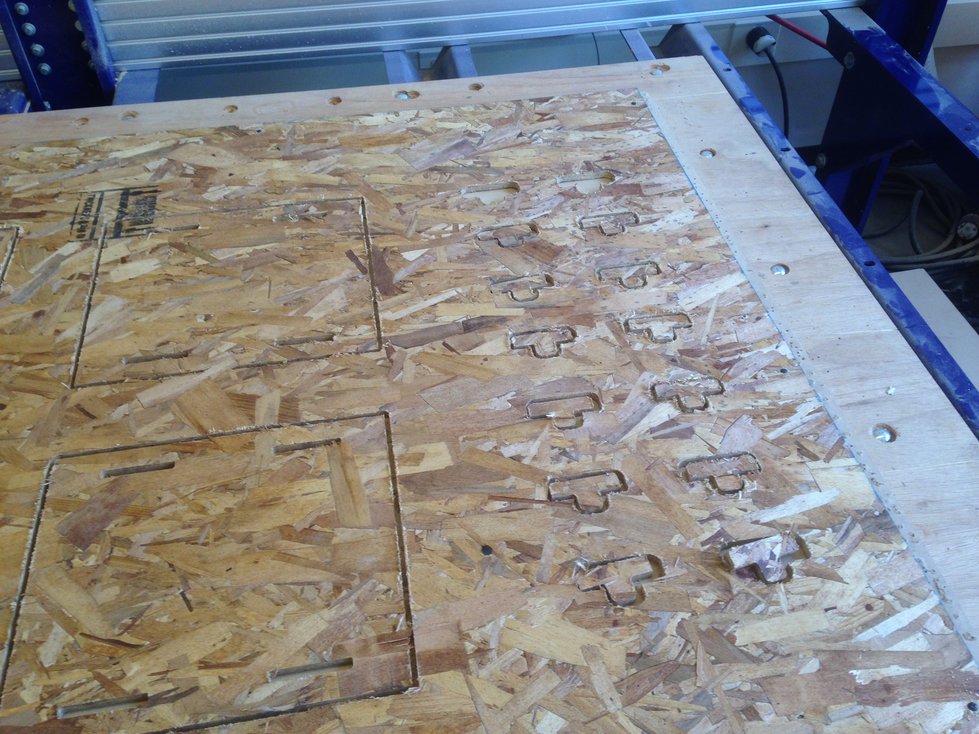
Luckily, this only happened to one piece. I recreated a toolpath for the lost
piece, making sure to include a couple more tabs, and I machined a replacement.
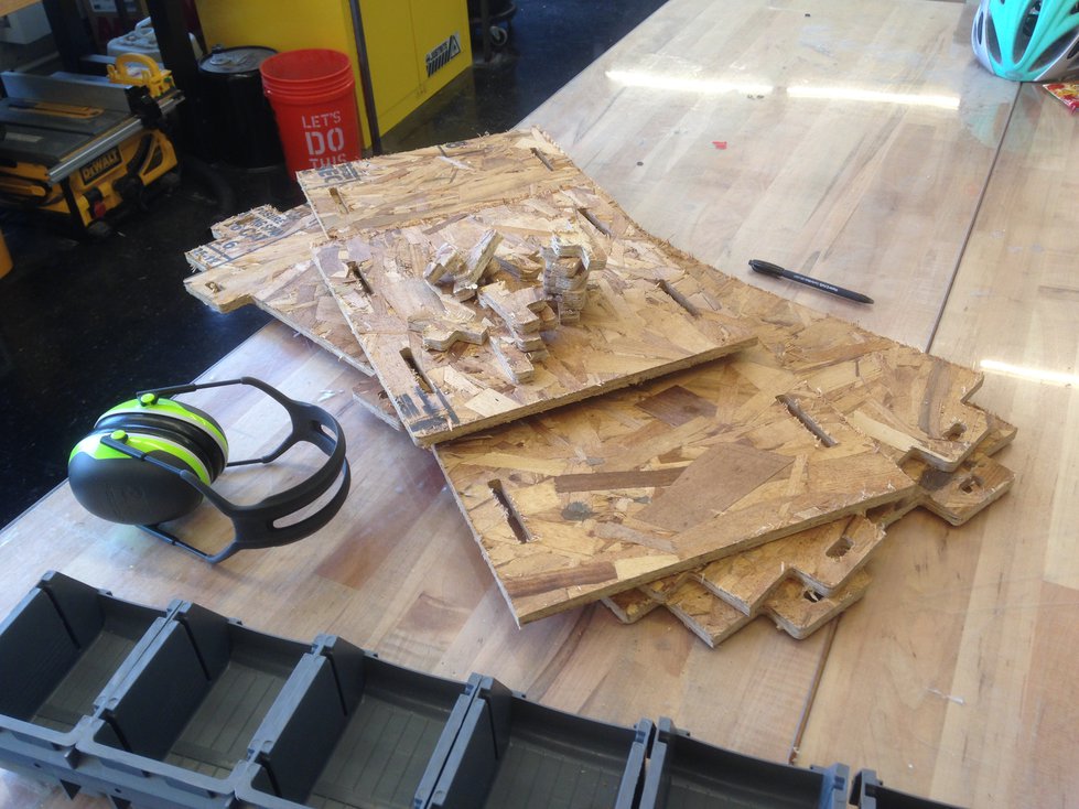
Here’s a picture of the board with all my pieces removed:
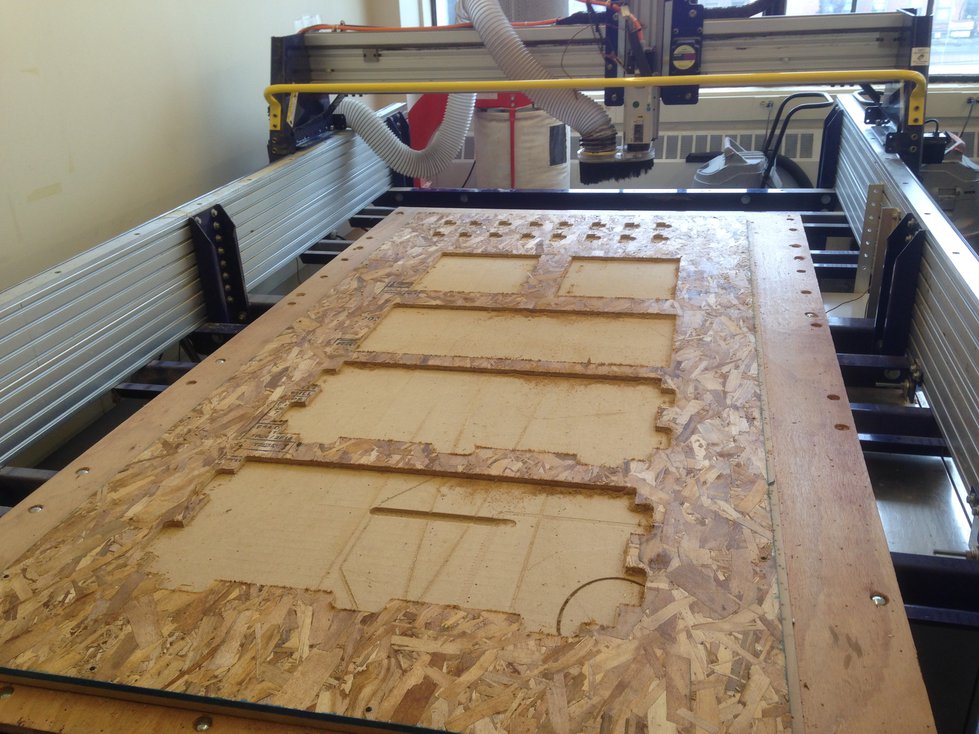
And here are all my parts:
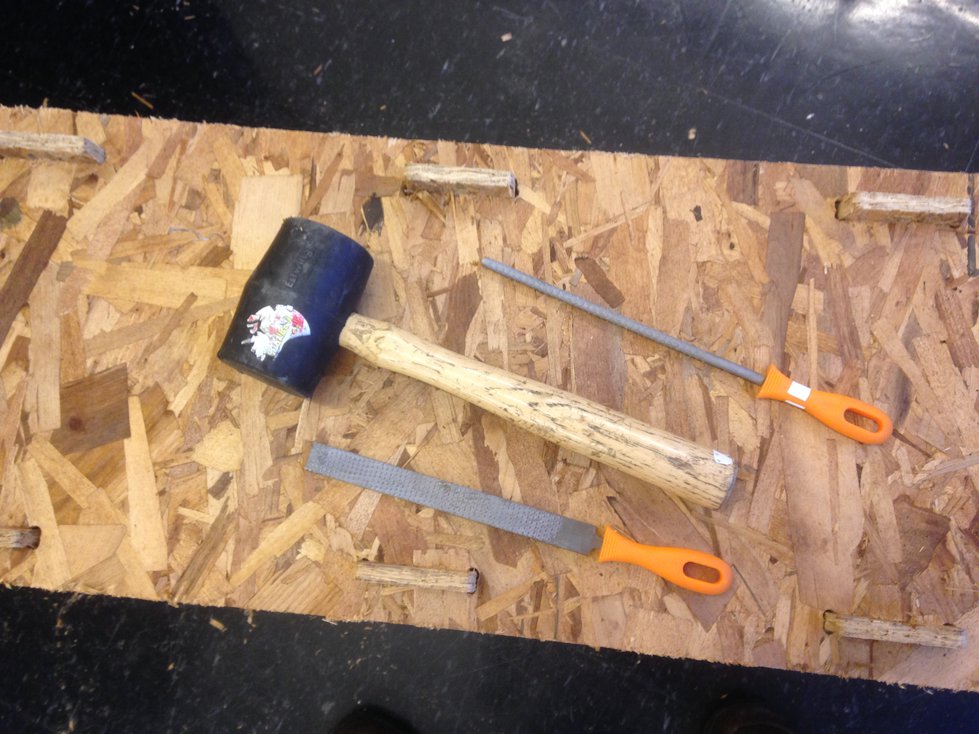
I realized that my parts didn’t fit together quite right. Making everything fit
required some manual dogboning using a wood rasp and some hammering together
with a mallet:
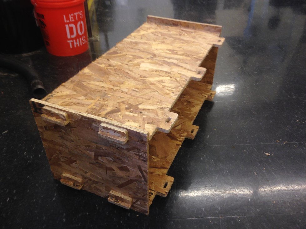
Here’s a shot of assembly in progress:
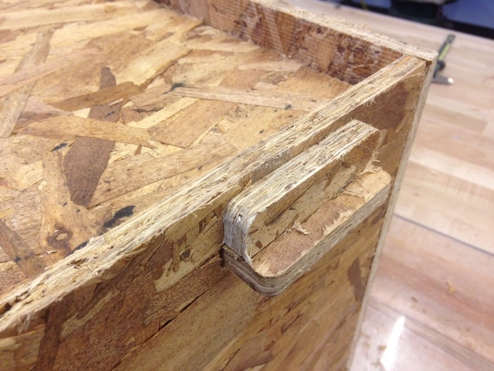
And here’s a close-up of a joint:
Result
Here’s the final result — a shoe rack, fully assembled:
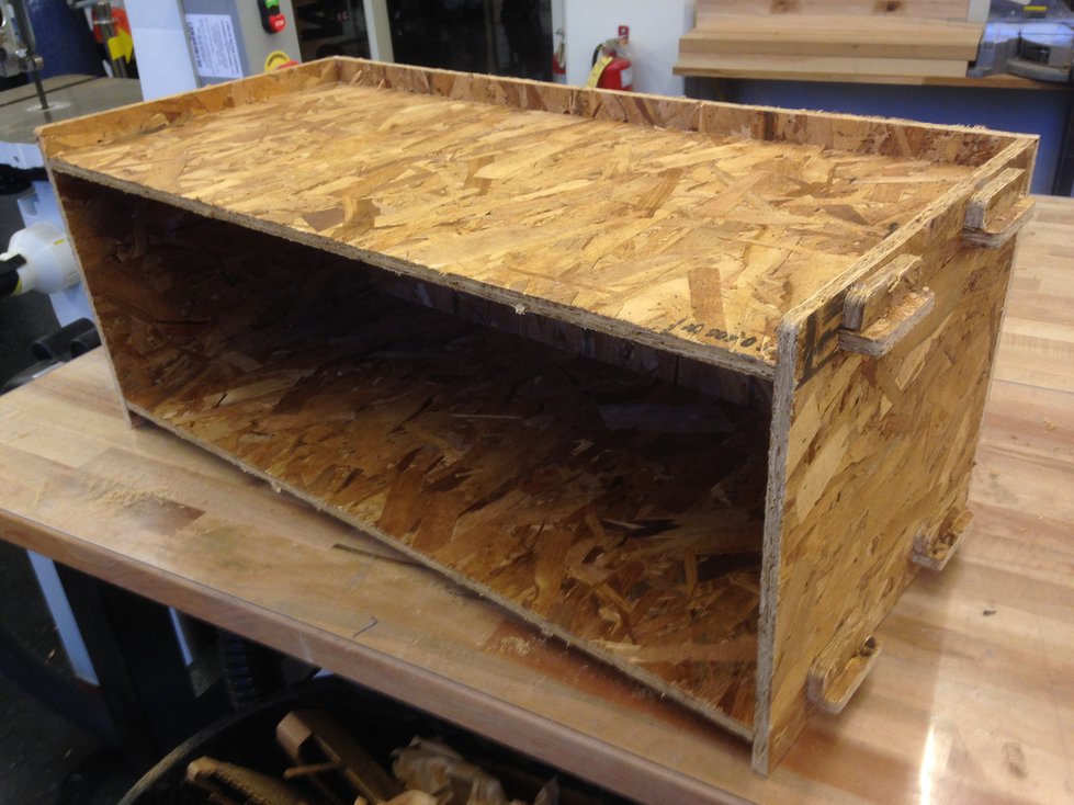
It turned out really well — everything fit very snugly — it didn’t wobble
or anything. The whole project came together without using any wood screws,
nails, or glue!
12 Oct 2016 · 4 min read
This week’s assignment was to redesign the echo hello-world
board
and fabricate the modified version.
I decided to use the EAGLE PCB Design software, because
it seemed like an industrial-strength tool for PCB design. Also, I had used it
once before (just for making schematics, though), so I was more familiar with
it than I was with other tools!
Schematic
I started out replicating the schematics of the echo hello-world board:
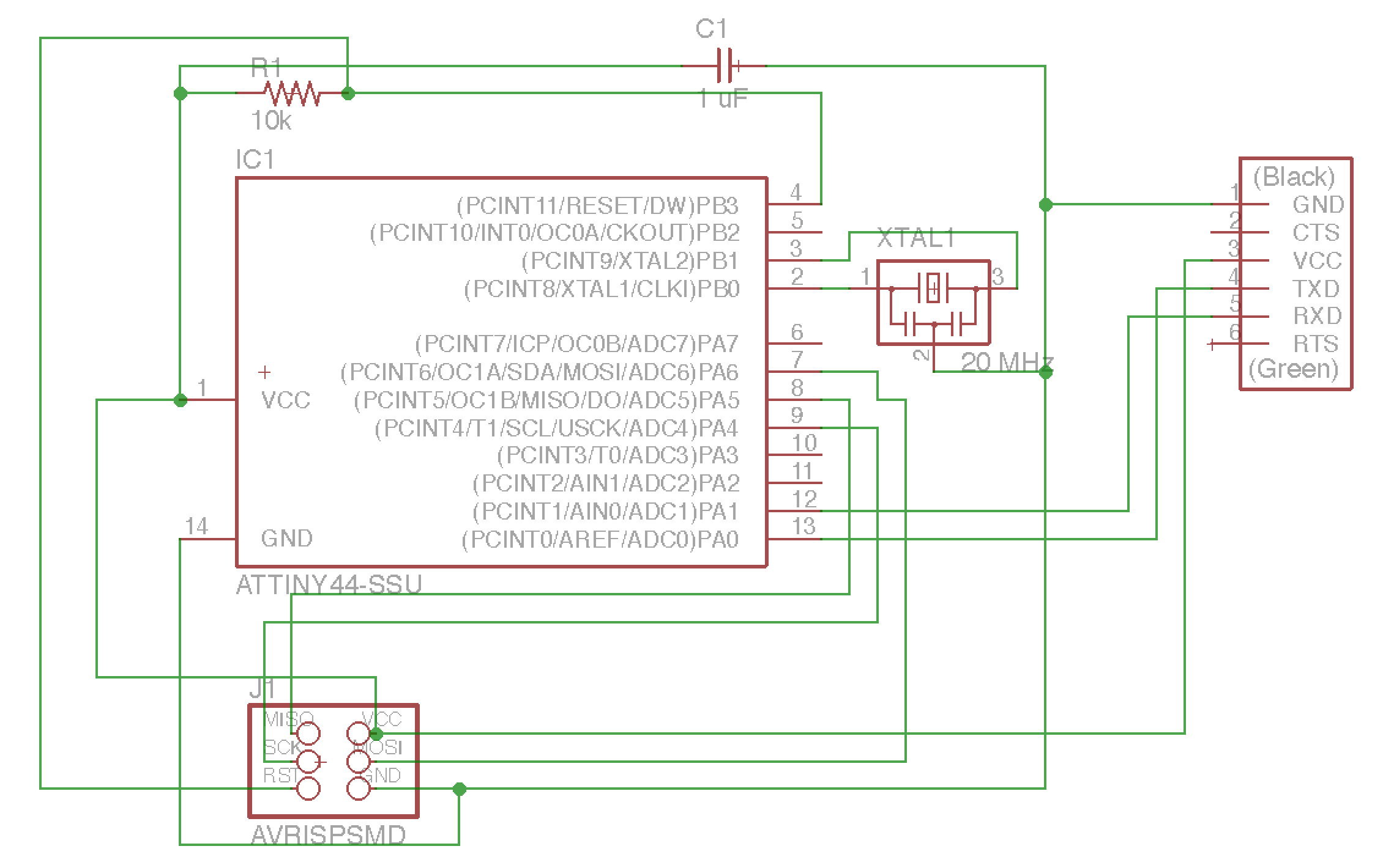
I added a button and an LED to the design.
When adding the LED, I made sure to put it in series with a current-limiting
resistor. To estimate the resistance required, I considered using a blue LED,
which has a voltage drop of about 3.4 volts. With a desired current of 5 mA
through the LED, a (5 V - 3.4 V)/(5 mA) = 320 Ohm resistor is required.
When adding the button, I decided to use a pull-down resistor configuration.
Essentially, the microcontroller’s input should always be driven high or low,
and using a pull-up or pull-down resistor with the button is a way to achieve
that. I chose to use a 10k Ohm resistor.
Here is the final schematic with the button and LED added:
Board Layout
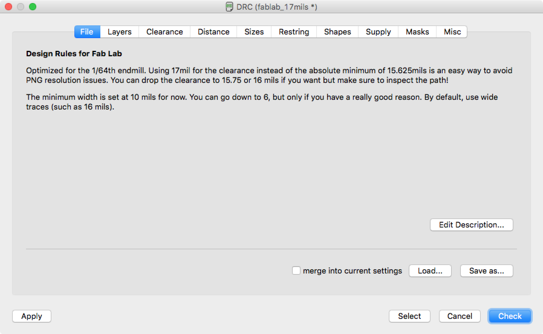
After designing the schematic, I did the PCB layout and routing. The first step
was to import the Fab Lab PCB design
rules
into EAGLE so that the design would be optimized for the 1/64” endmill used on
the SRM-20 (which would be used later for production):
Next, I laid out the components on the PCB and tried to use EAGLE’s autorouter,
which attempts to automatically figure out how to wire everything together
while respecting the design rules and avoiding things like crossing wires. By
default, the autorouter uses 2 layers, but I disabled the 2nd layer, which
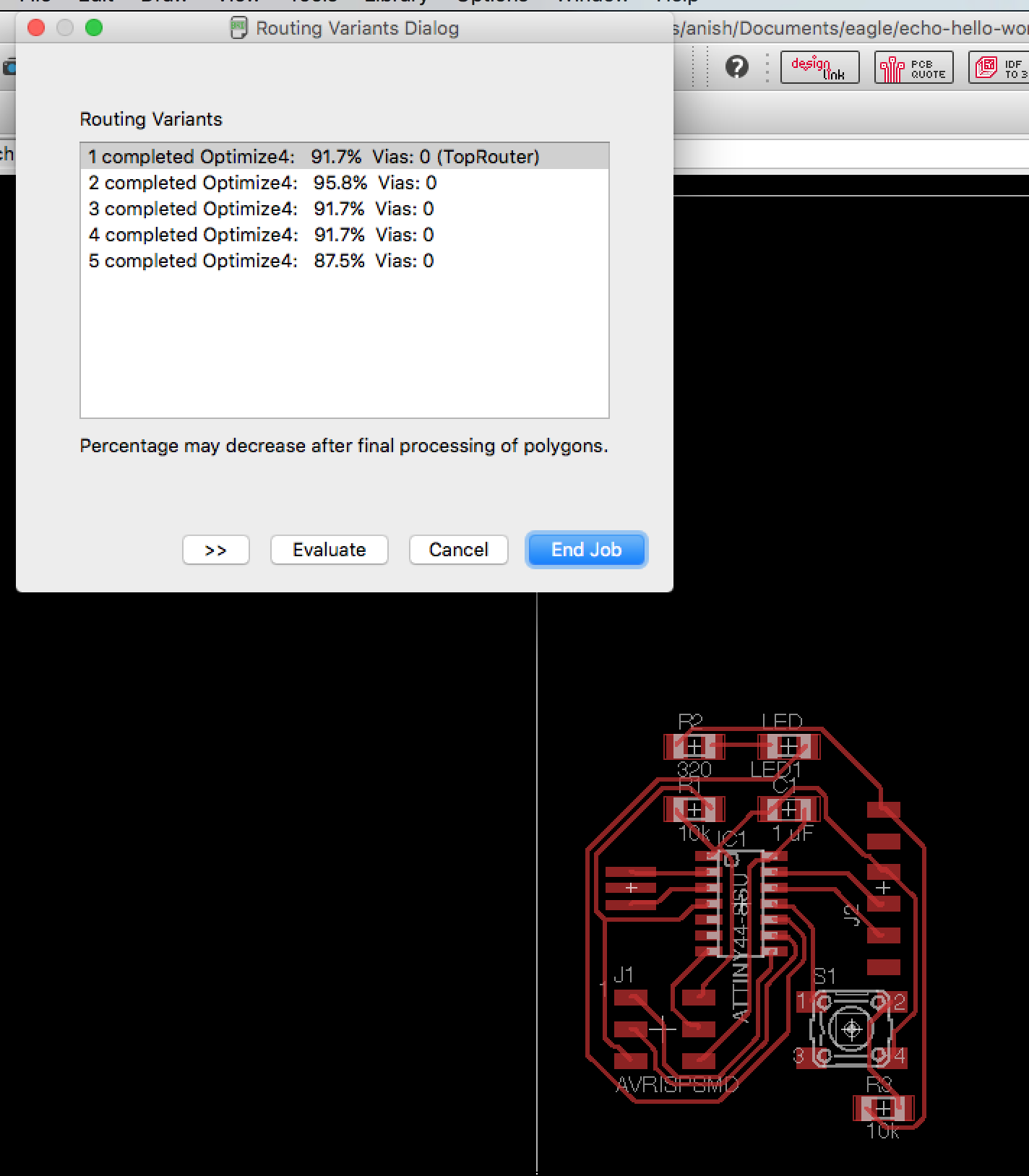
forced the autorouter to route for a single layer PCB. In my first try, the
autorouter couldn’t route all the wires (none of the routing variants are at
100%):
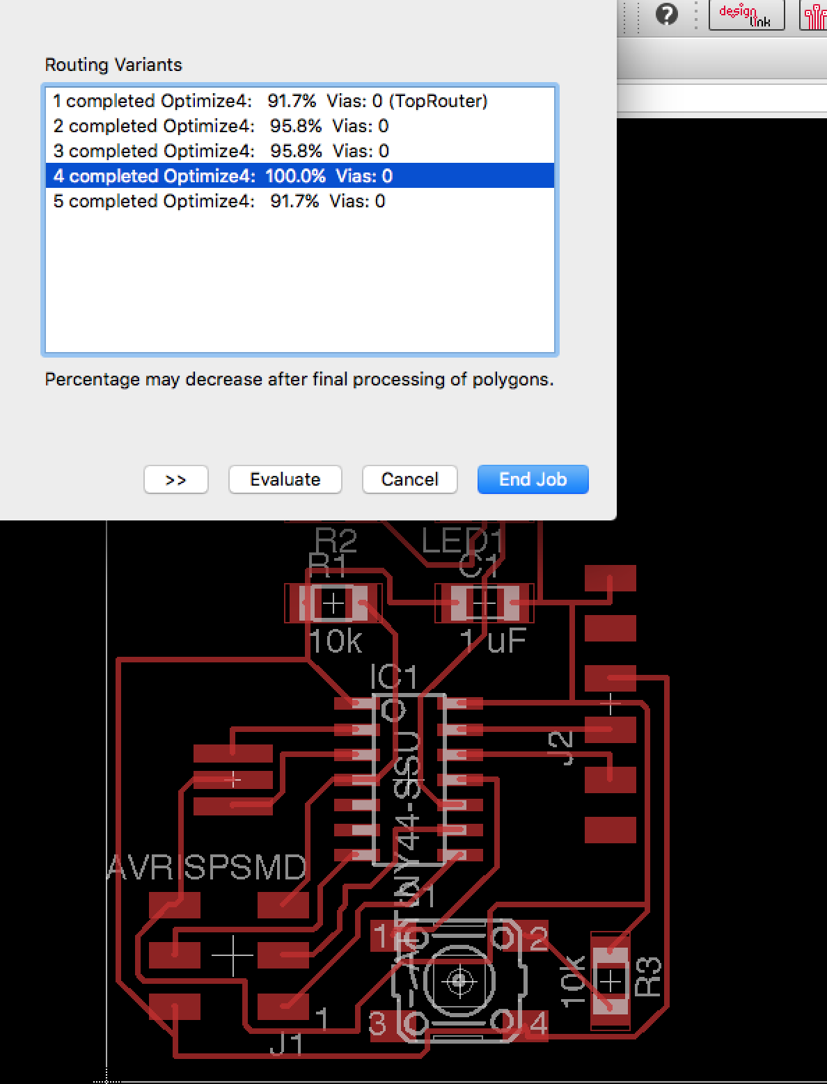
After moving and rotating parts to try to improve the design, I tried the
autorouter again, and it managed to route all the traces:
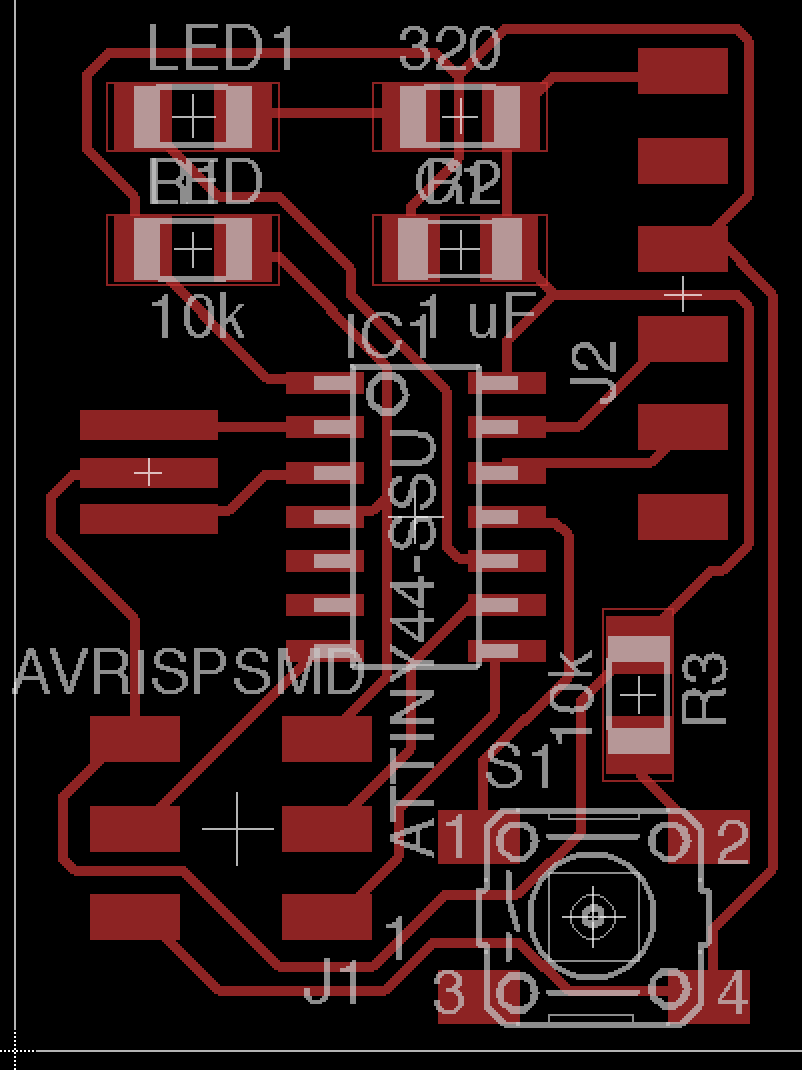
Now that I knew that routing was possible and that the autorouter could find a
valid routing, I played around with the design to try to get it to be a little
more compact. Here are the final results:
Exporting
Now that I had a PCB layout I was happy with, I needed to figure out how to
export it so that I could mill a PCB. Eagle can export PNG images of PCBs — I
just needed to disable all the other layers in “View > Layer Settings” so that
I could get a clean image.
I exported an image at 1270 ppi, imported it into Photoshop, cropped it
slightly, and made a 64 pixel border for the PCB outline. Here is the final
result:
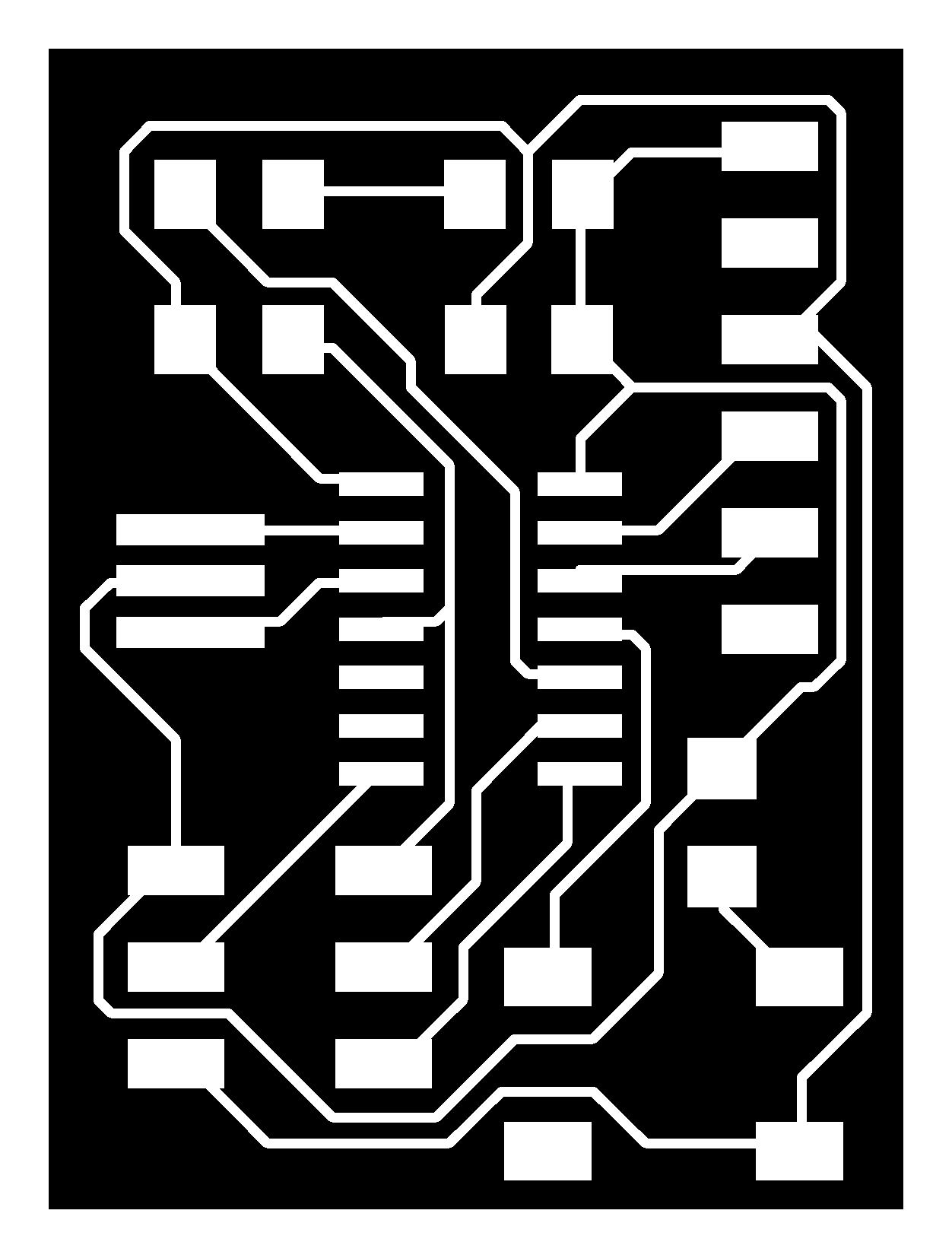
The traces can be found here, and the outline can be found here.
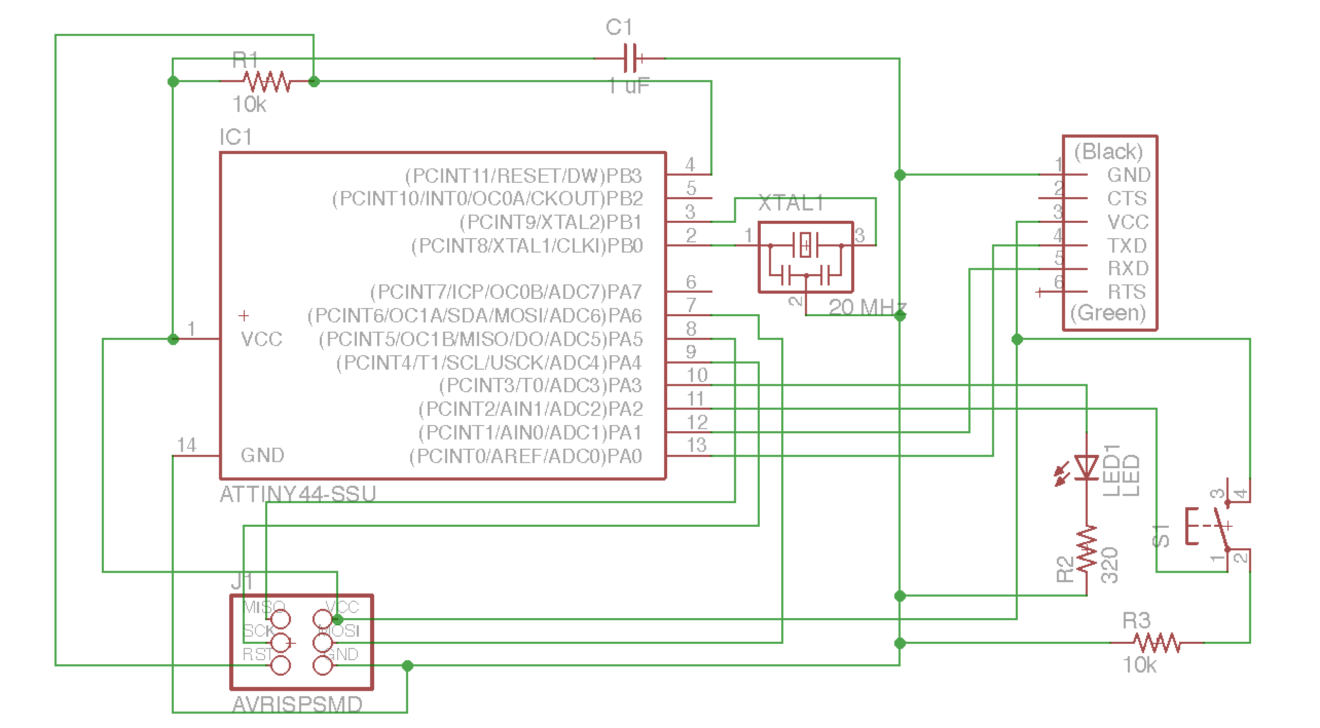
Fabrication
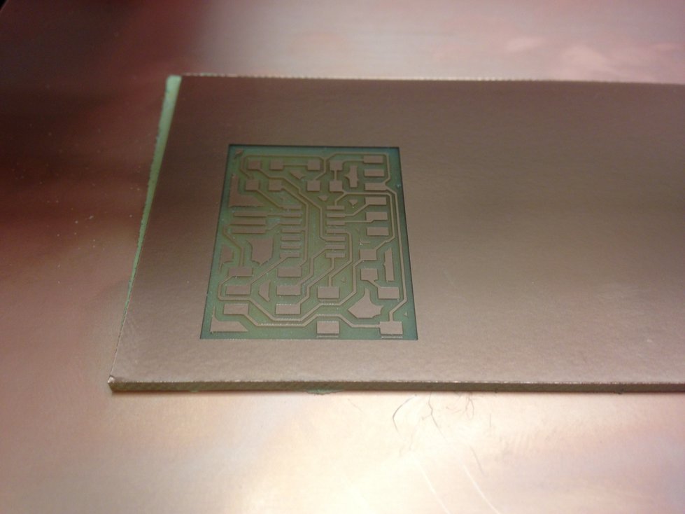
Using the same methods used in week 3, I fabricated a PCB. Here’s the
freshly milled board, about to be removed from the SRM-20:
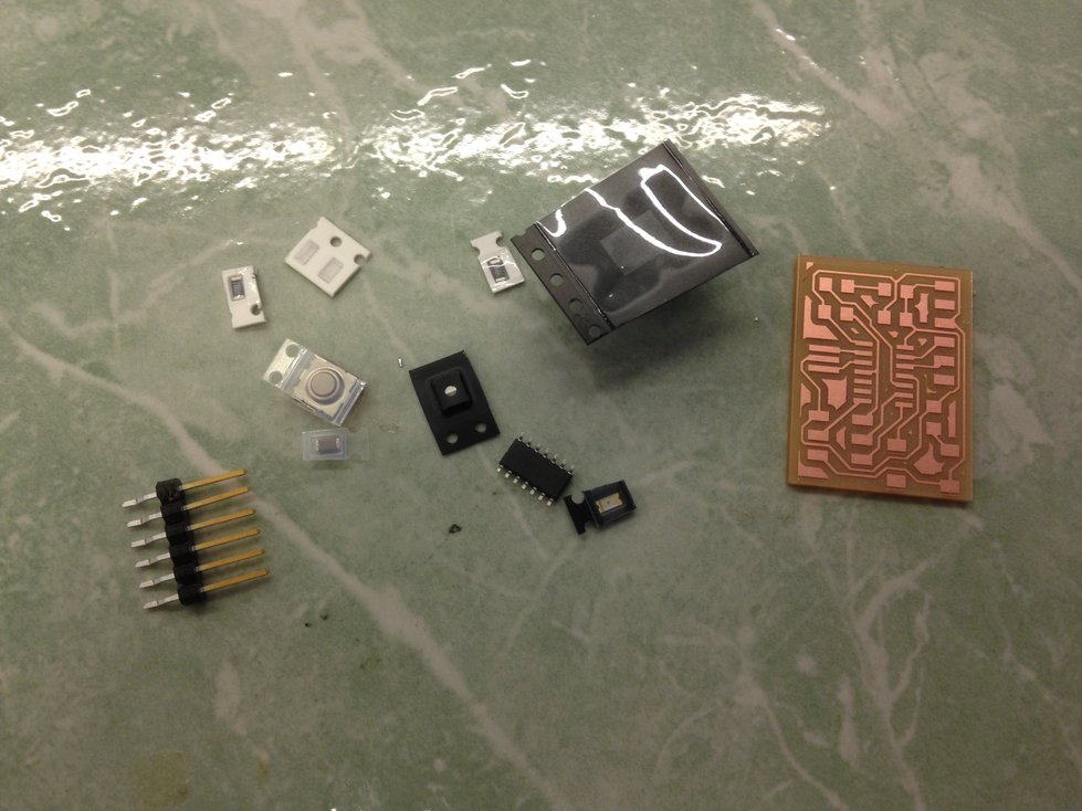
Choosing components for the board, I made some slight modifications to the
design:
- Chose to use an orange LED, which has a voltage drop of about 2.1
volts
- Chose to use a 499 Ohm resistor with the orange LED for a current of (5 V -
2.1 V)/(499 Ohm) = 5.8 mA through the LED
Here is the PCB and components, ready to be soldered:
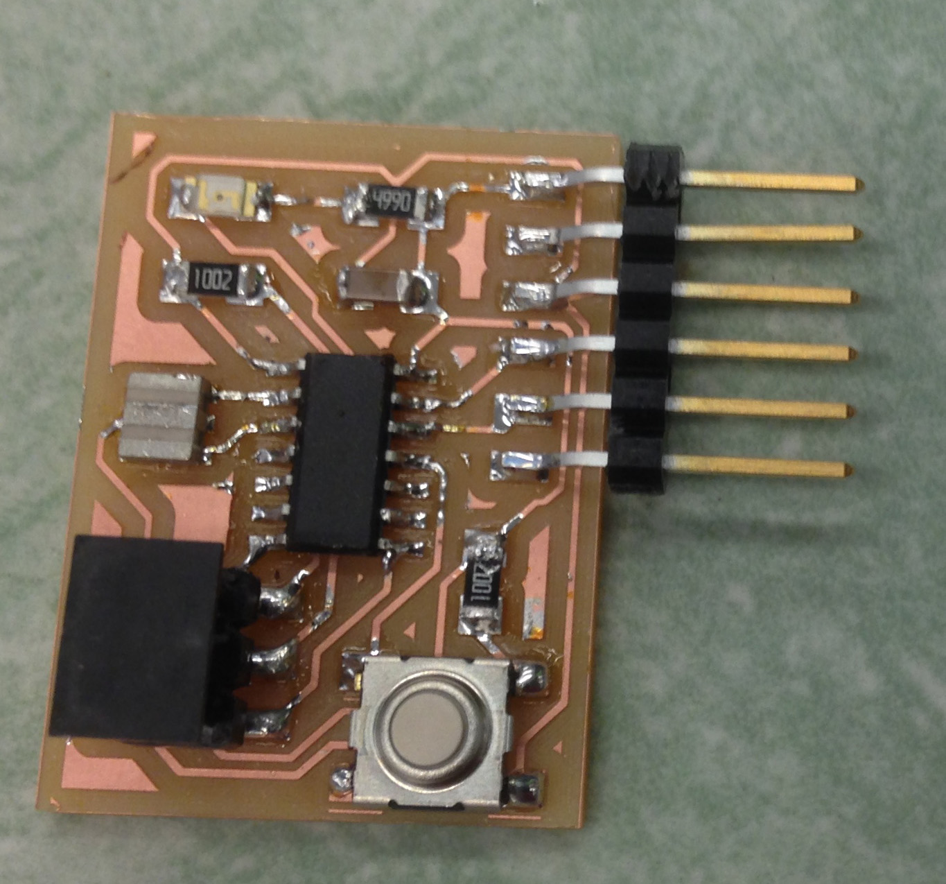
Here’s the final result:
05 Oct 2016 · 3 min read
3D Printing
The assignment for this week was to 3D print something that could not be
manufactured subtractively.
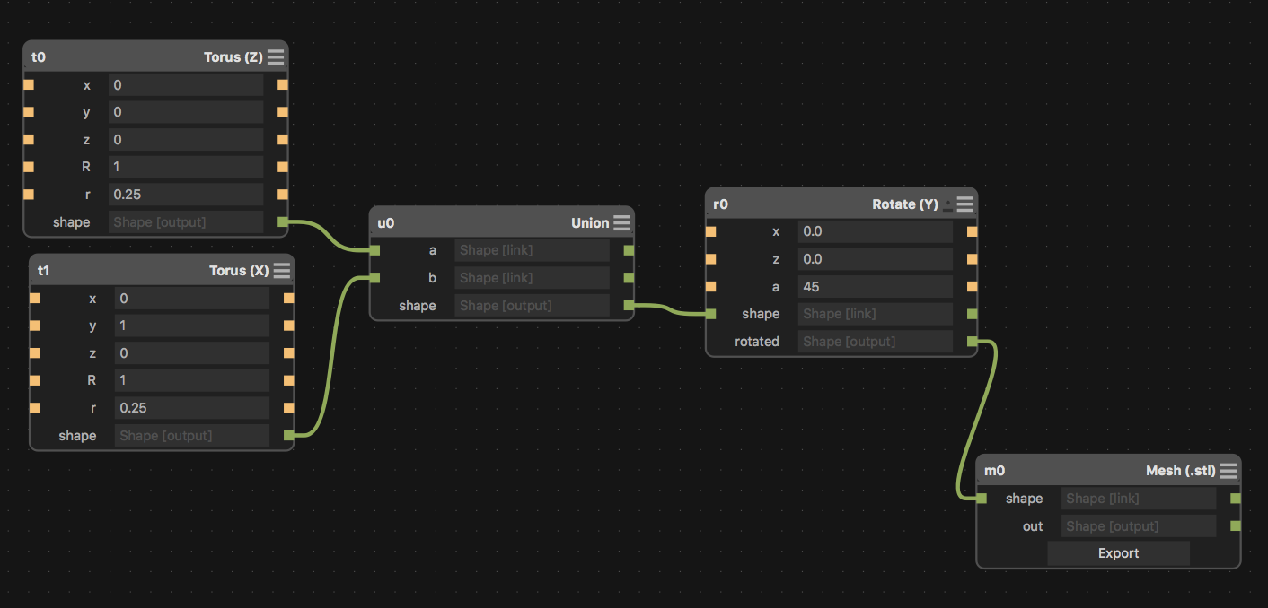
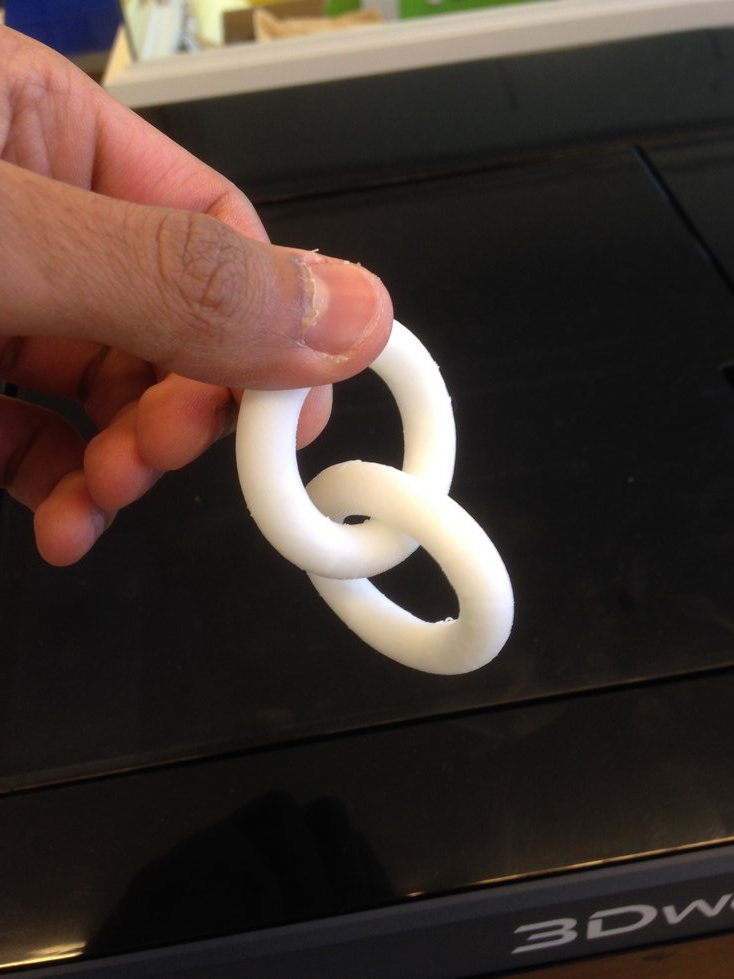
I chose to make a pair of interlocking rings. It was very simple to model using
Antimony as two identical toruses
positioned appropriately with respect to each other:
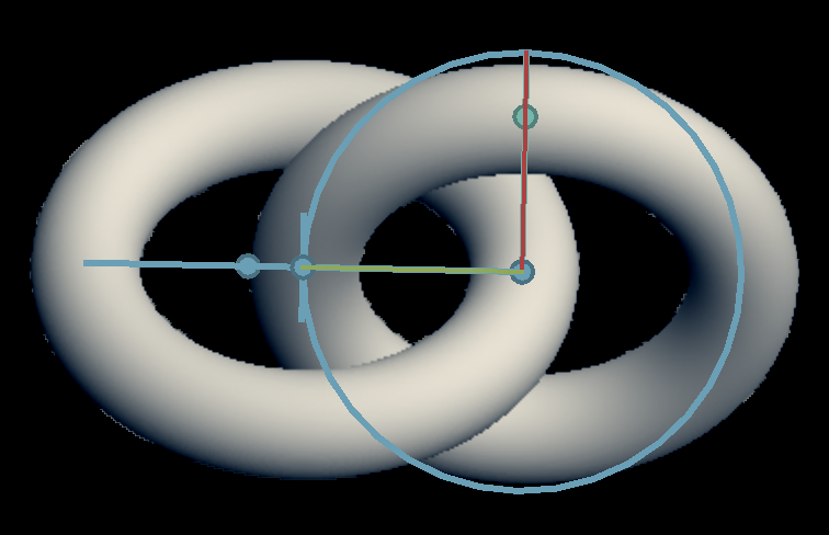
This is something that couldn’t be done subtractively. It also couldn’t be
produced as two parts and joined together later, unless one of the rings was
cut, the parts were put together, and then the ring was glued back together.
Printing Process
I printed my piece using white PLA. I used the Sindoh 3DWOX printer, which only
supports using a single material, so the same PLA was used to create support
material too. I used the 3DWOX Desktop software to import my STL file, rescale
it to a reasonable size, and print it. The software was very straightforward to
use.
I knew that printing this piece was going to be somewhat tricky, because it’s
pretty thin and narrow, and there would be a lot of freestanding mass. Before
printing, I oriented the toruses so that height was minimized:
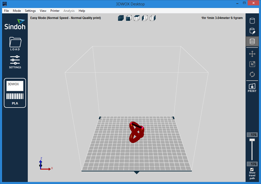
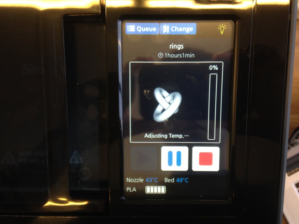
The piece only took an hour to print:
Finishing Touches
The piece came out really well, even though it used almost no support material:
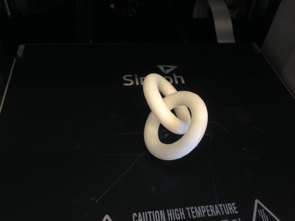
It only took a moment to remove the two small pieces of support material:
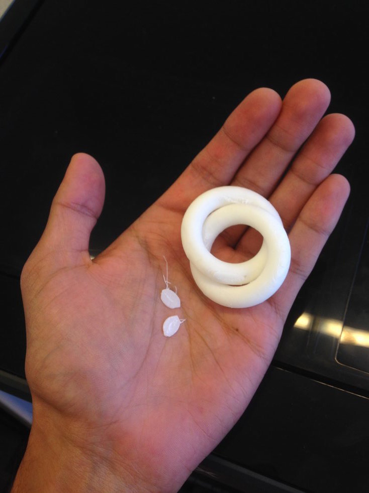
Result
I was quite happy with the result. It’s simple, but it’s still an interesting
piece that’s gotten a “how did you make that?” when I’ve showed it to people.
3D Scanning
I did photogrammetry using Autodesk 123D Catch.
I scanned two wire cutters propped up against each other:
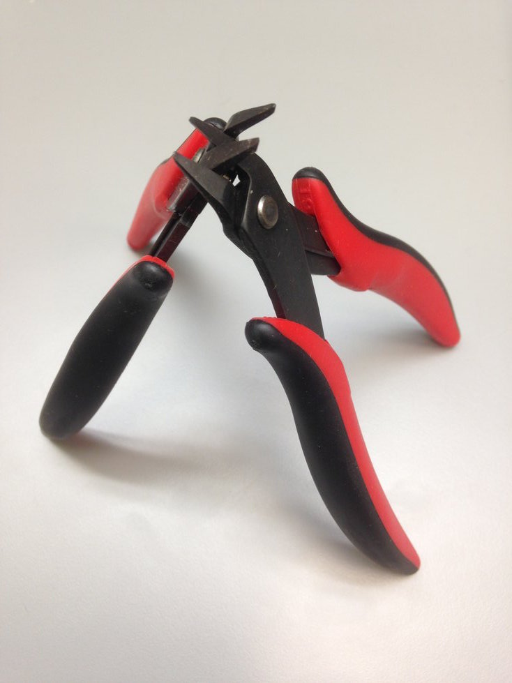
After taking about 30 photos from various angles, I let the software process
the photos, which took quite a while (it took an hour, but that might have been
an anomaly). Here’s the result:
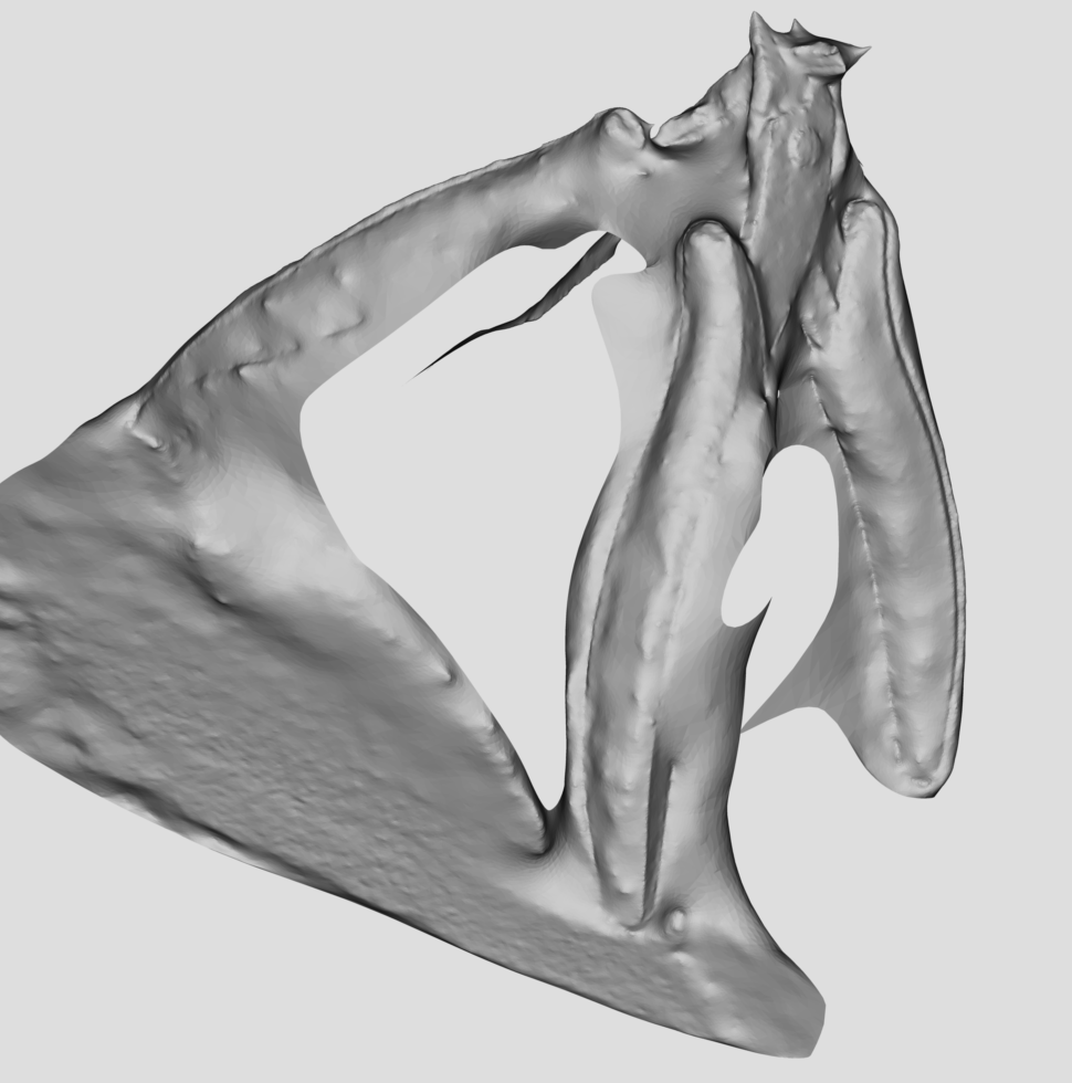
In hindsight, this scan was probably too complicated for iPhone-based
photogrammetry. It’s far from perfect, but it does capture the basic geometry
of the object. And the top of the wire cutters actually came out quite well.