Electronics Production

For this week, our assignment was to design and build a PCB. I made some very wrong choices with this assignment, I think, which cost me to spend a lot of time on things that could have gone much more quicker than they should have. So, to all those reading this in the future, please pay extra attention.
In the every begining, I was very ambitious. I wanted to fabricate a three dimensional circuit that looked like a palm tree. So I made the model with Solidworks, but then realized that exporting it into KiCad or Eagle was not be as easy as I thought it would be.
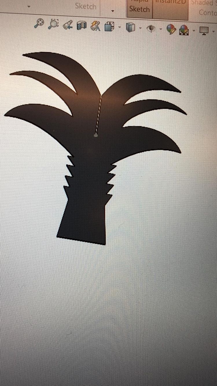
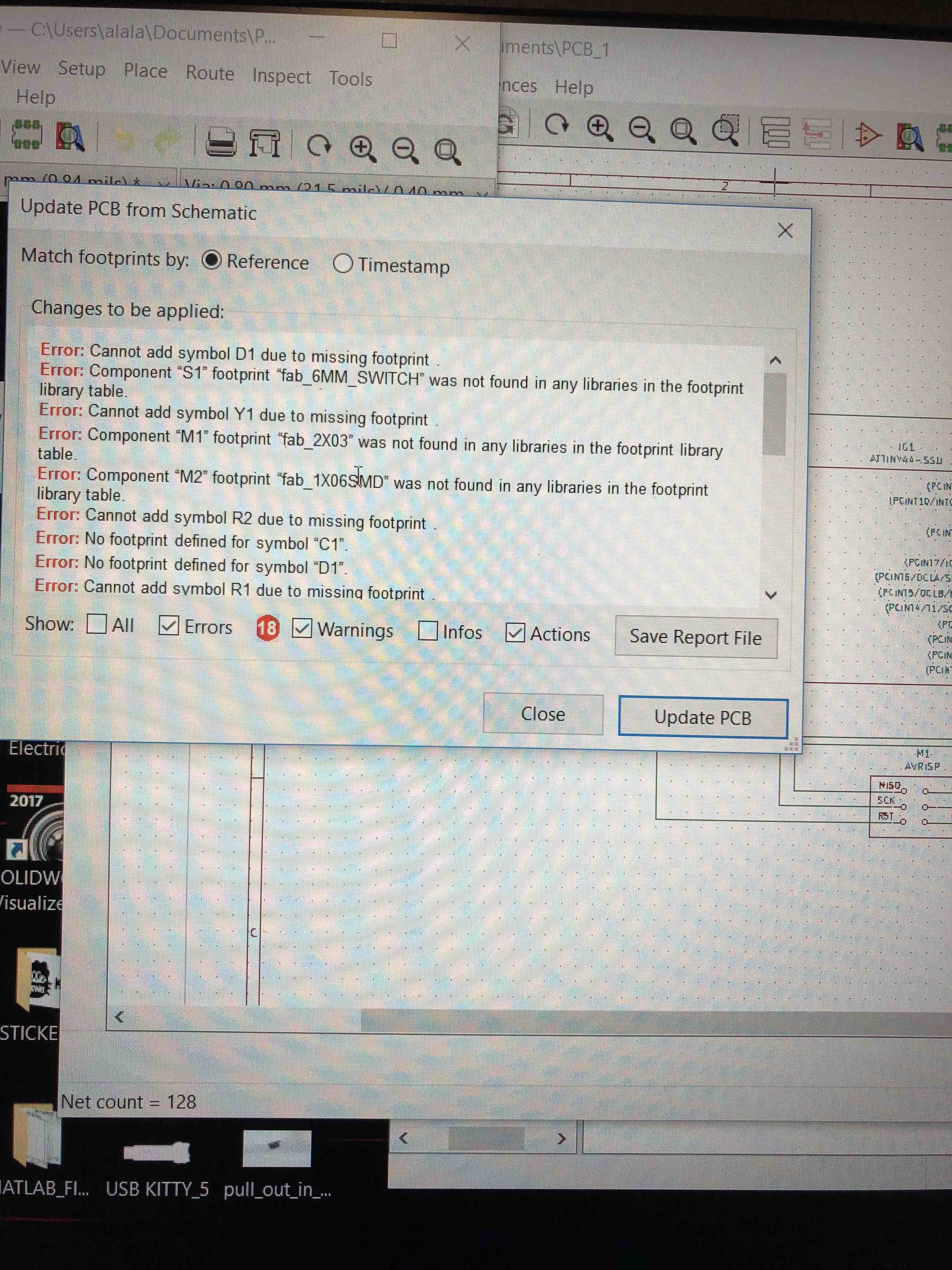
So, I scratched the idea for the time being, though I hope to implement it during "Make Something Big" week. I used KiCad to build my circuit from schematic to PCB, which actually took more time than it should have. I had some problems with KiCad recgnizing the imported library when I was assigning footprints , although the library was in the correct path, and with the correct ".pretty" extension. I spent around 10 hours debugging this (plus or minus because I was tired at that point), but couldn't solve it. At the very end, I had to manually set the footprints for the sake of time.
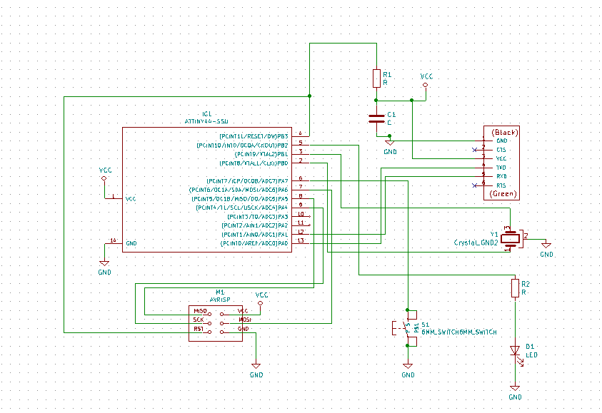
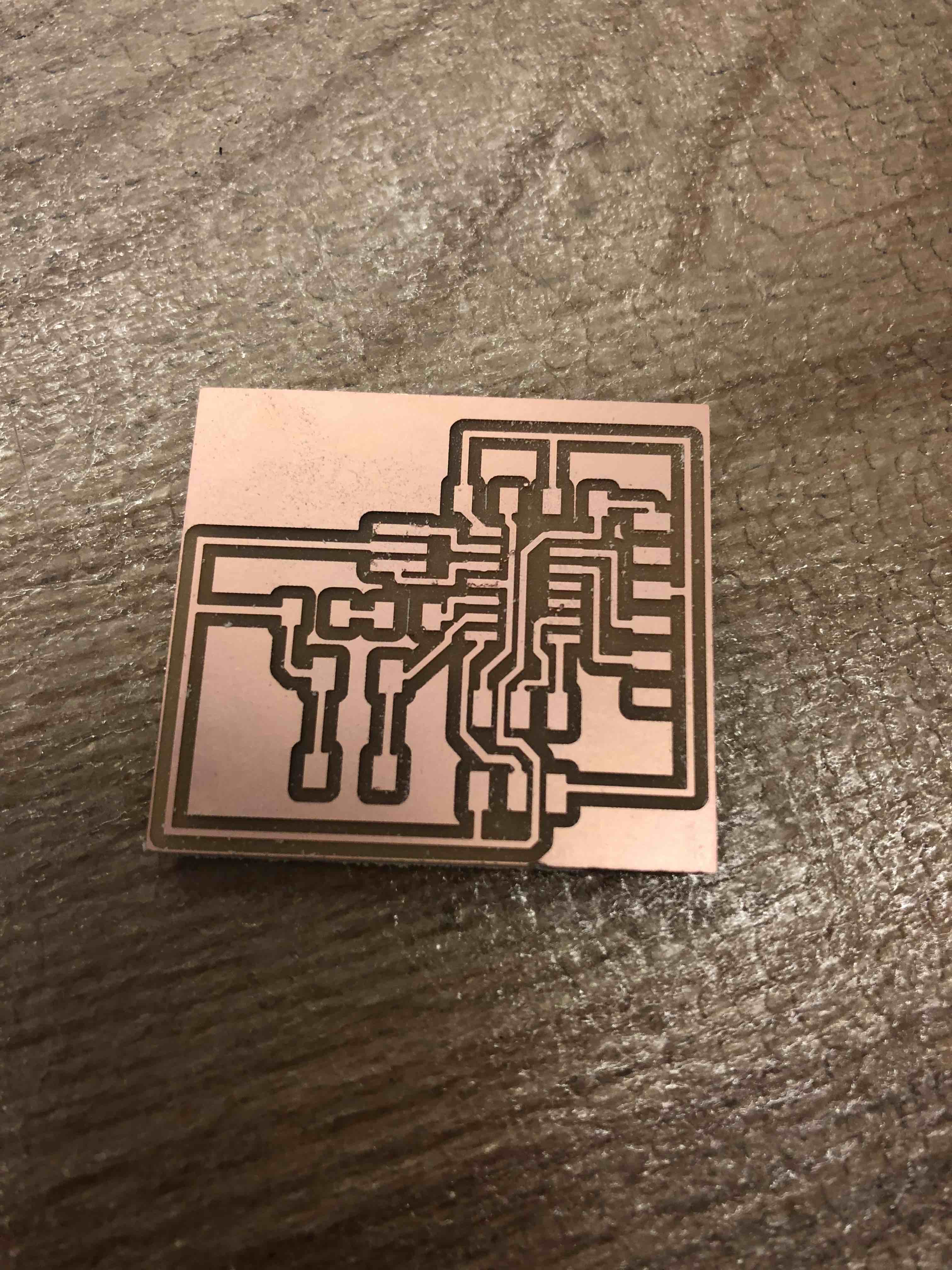
So, when I had my schematic in PCB mode, all I had to do was draw the traces. I forgot to check the design rules, and drew all my traces with 0.25mm. Before fabrication, I realized this, and had to change and redraw my tracks to 0.4mm again from scratch (Make sure you check the design rules!!)
Another problem was that KiCad automatically put the spacing between the pins on the Integrated Circuit (ATTINY44) to be really small, which limits, and makes it VERY difficult to draw nice traces/tracks. So, Zach helped me change the spacing by changing the model in the library (yes, you can do that, and it will not reflect negatively later. Microcontroller pins/legs extend). Thus, my PCB design was done.
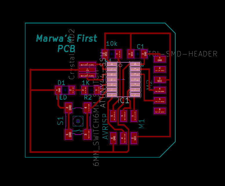
Although I had come in the aftrenoon to the shop to mill, I didn not anticipate the time it would take me and the others to mill, remill, solder, re-solder, and program. I eventually milled my board, and soldered it correctly so it works, but I didn't have time to actually program it.
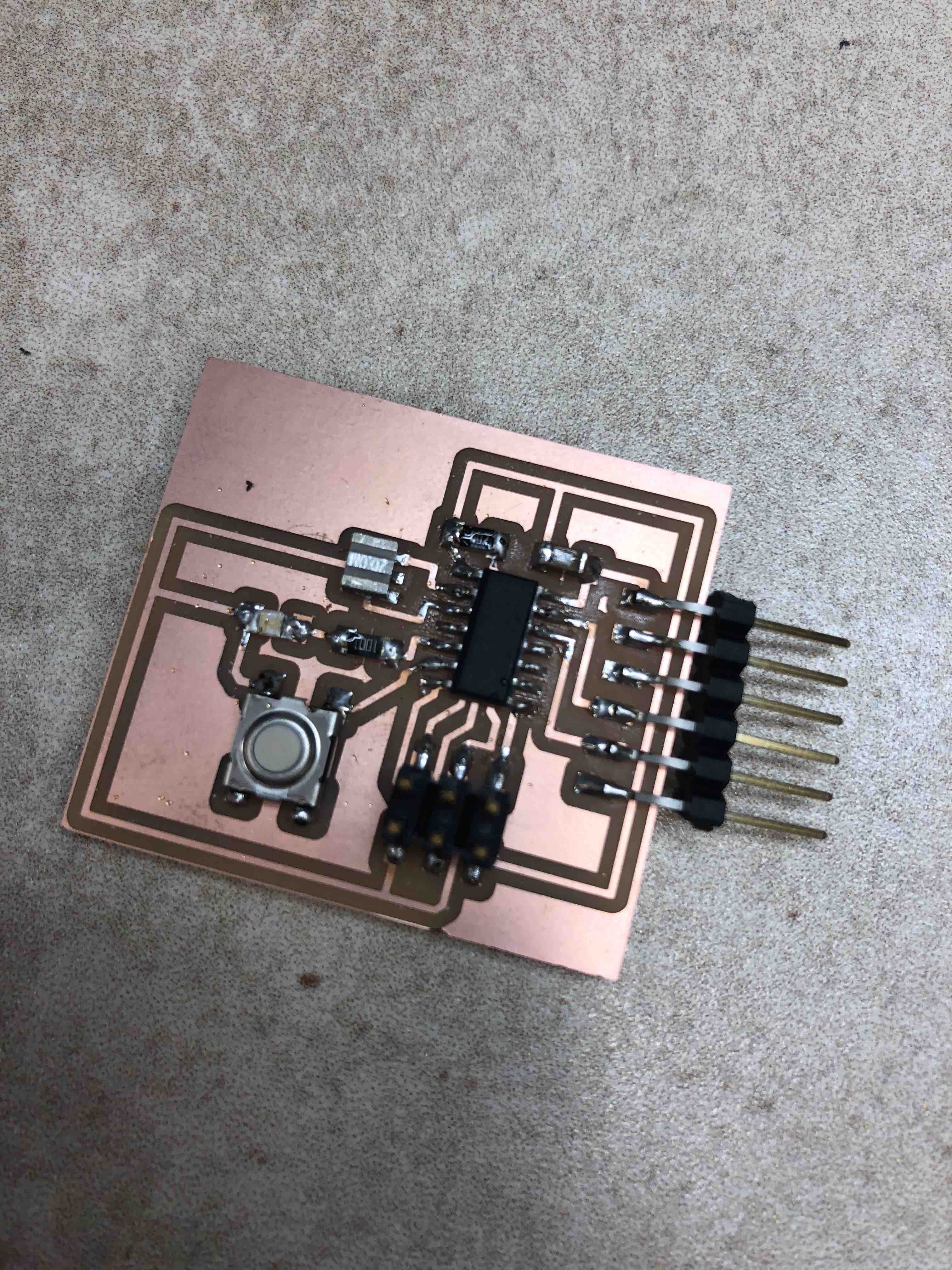
Note: I have already programmed this board in Interface Week, and also during week four. However, documentation for week four programming (using Niel's Code) was lost as my phone was unfortunately stolen.
Download Board Trace
Download Board Border

.