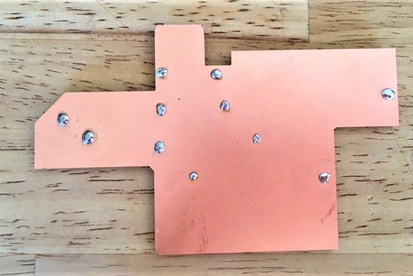
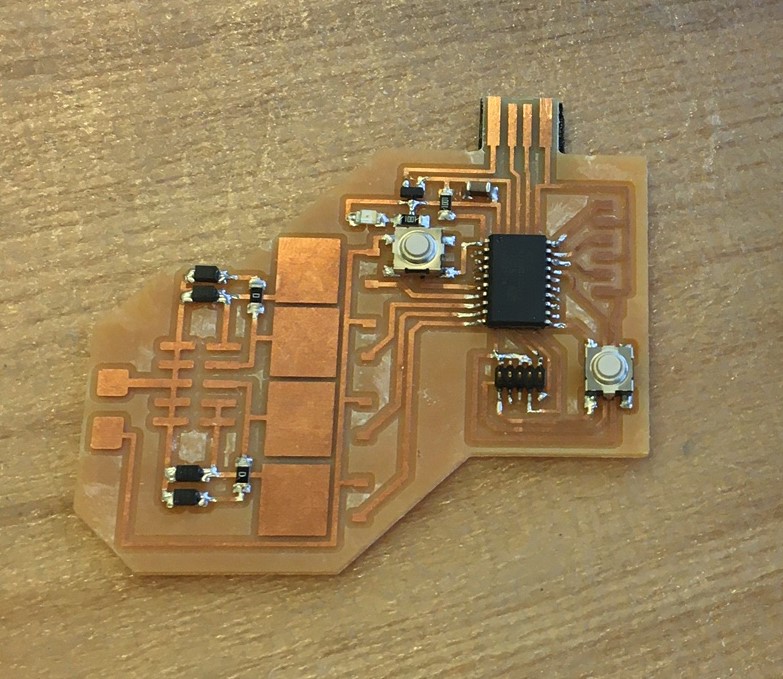
Home Final Project Week 1 Week 2a Week 2b Week 3 Week 4 Week 5 Week 6 Week 7 Week 8 Week 9 Week 10 Week 11 Week 12 Week 13 Week 5 Assignment: Electronics Design
Week 5: Electronics Design
5.1 Introduction
As with most facets taught during this class, PCB design was a completely new topic for me. Having used Fusion 360 previously, I decided to use its Eagle package for designing my PCB. For milling I used the same Roland SRM-20 end mill described in Week 3. In the design of my PCB, I wanted to incorporate capabilities that could be used for testing my final project prototype. Programming this board would be beyond my current capabilities, but developing a functional layout with MOSFETs, motor diode protection, and pull up resistors were the learning objectives for me this week.

Autodesk Eagle Application

5.3 End Milling - Round 1
After altering the display of my schematic document in Eagle, I used the export image function to create monochrome .PNG trace and outline files with a resolution of 1000 dpi. Images of these documents are shown below and both are individually hyperlinked.


Milling the traces of my board with a 1/64 in end mill progressed well, except for one 10 mil ground trace from the programming header that lifted (circled in red on the image to the right). Based on the end mill design rules completed during week 3, I did not expect this to occur. I failed to inspect the end mill prior to milling and suspect copper debris build up on the end mill may have caused with discrepancy. However, to help prevent this in the future I would recommend increasing trace width and/or .PNG file resolution to limit 'staircasing' along angled trace runs. While milling the outline with a 1/32 in end mill, I immediately noticed a discrepancy while milling the board's vias; they were significantly oversized (circled in yellow on the image to the right). After recognizing this I stopping further milling of the outline.


With several students waiting to use the micro end mills in the EECS lab, I decided to remove my board rather than attempting to correct via sizing on the .PNG file. I used a drill press to finish drilling via holes and a band saw to cut the board’s outline. From here I proceeded to weeding and deburring the board with tweezers, needle nose pliers, and a razor blade.

5.5 Via Hole Sizing Quandary
After reviewing my schematic in Eagle, I found I used vias with an outside diameter of 32 mils, which is nearly equivalent to the diameter of the 1/32 in (31.25 mil) end mill being used to create them; this checks out. In looking closer at the via component symbol, which is shown to the right, I realized while adjusting color of my .PNG outline file in Paint, I used diameter 2 instead of diameter 1. With this correction I was more confident with via sizing going into round 2 of milling my board.

5.7 Soldering - Round 2
After soldering vias into place, I verified continuity of all ground traces to the bottom layer with a multimeter. My general soldering skills are gradually improving, but I still struggle with heat control and patience. I then discovered another discrepancy in my design, the USB port was slightly oversized. I removed excess material from the USB port with sand paper, but pulled off a jumper connection in the process (pads and all); luckily I had immediate plans for using this.


5.9 PCB Fabrication - Round 3
I will not bore with the details of Round 3, but have provided images and file hyperlinks below. I made several alterations to the design, such as MOSFET heat sinking and ground trace routing, but general functions remained the same. This board was successfully programmed and used for coding assignments during future weeks.


5.11 Takeaways