Weekly Progress
Week 4: Electronics Design
Designing an Echo Board with a Button and an LED
As a relative novice in electronics design, this week's assignment had a lot of new content for me. I attempted to do the baseline task which was to take Neil's schematic for a echo board with a ATSAMD11C microcontroller and update is with our on design while adding an LED and button. I used KiCAD (a great open source tool for circuit desgn) to design the schematic and footprint of the board. I then milled my design onto a copper plate and prepared my components (collected from the lab for soldering. Unfortuantely, I ran out of time to actually add my components to the board, load the program and test my board before class this week -- I'll get to this asap to see if what I designed works! I'm sure it will be quite satisfying :)
KiCAD can be quite daunting when opening the page for the first time. Luckily Jake and Zach's recorded recitation provided some great guidance to move through slowly and and watch as a moved from step to step.
Step 01: Designing the Schematic
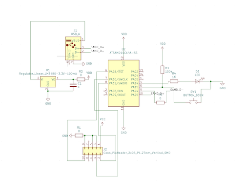
The idea here is to lay out all the components we'll need for our design and connect them. This isn't the footprint (i.e what the board is going to look like), but will define the set of relationships we will use when designing the footprint. We have been provided with a KiCAD library that has all the components we might be using in class and that are available to use through our fab labs. KiCAD also has some inbuilt libraires, though I found that for some reason my installatin of KiCAD did not include these libraries. I installed them as I needed from the KiCAD website (which ended up just being the power and connector libraries for the generic GND, VCC/VDD, USB components).
I was able to figure out which specific components (i.e what size/manufacturer) I needed by asking TAs and classmates, but now feel that I have developed some intuition for how this works. When the question is one of physical component size or manufacturer, see what is available in the shop. If the question is about how many pins you might need, see if you have additional pins and if there is a smaller component available. The size of resistors and capacitors and be calculated by understanding what the component is doing (ex. a pull up resistor). (Sometimes a little Googling helps.)
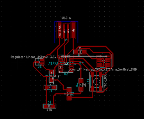
Step 02: Designing the Footprint
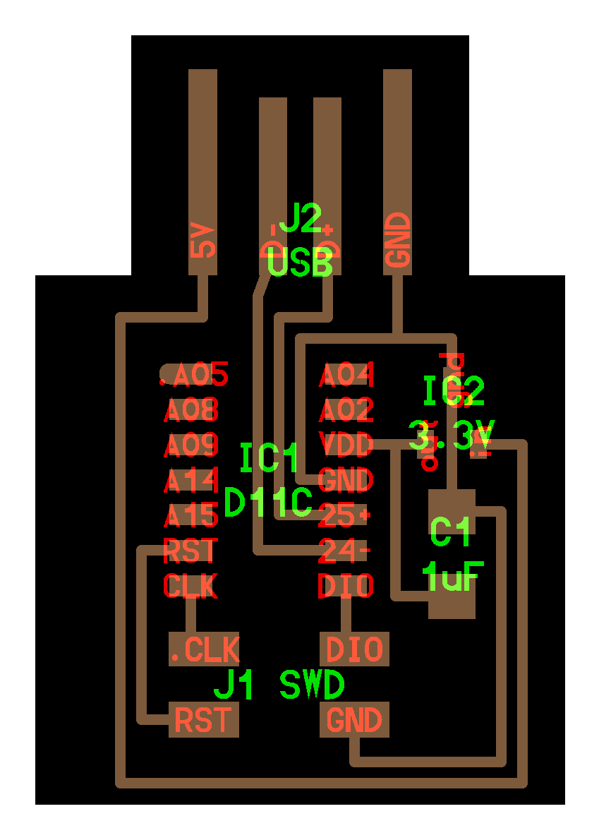
This part seems trivial, but involves some serious maze making skills to make sure you don't overlap any connections. Thankfully KiCad doesn't allow you to do this accidentally, but it is still frustrating when you can't make a conncection. 0 ohm resistors can be used to jump over traces, but ultimately that means using more components and more soldering later on, so this should be kept to a minimum. As you add these jmp components in the schematic design, you can update the linked file in the KiCAD footprint designer.
This is one of many attempts that almost got there, but ultimately failed.
4 or 5 more attempts later (starting from scratch), I finally found success!
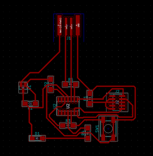
I exported my board outline and the traces SVG's and perpared my files to mill.


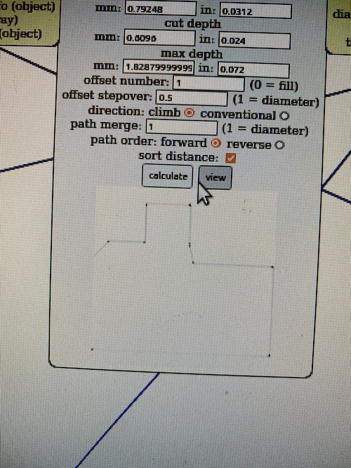
Part 03: Milling
You can see my Week 02 page for more details on the milling process. As with last time, I milled my design on a copper plate using a 1/64th endmill for the traces and a 1/32nd endmill of the outline (using the MODs interface).
I did run into one problem. For some reason, MODS was unable to complete the tool path for my outline and as a result did not fully cut out my part.
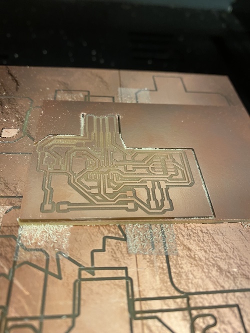
This red line on the preview of the tool path should have been a warning, but I didn't relaize that meant it wouldn't run...I'm curious how to solve this issue and why it may have occured and will ask.
Part 04: Soldering/Conclusions
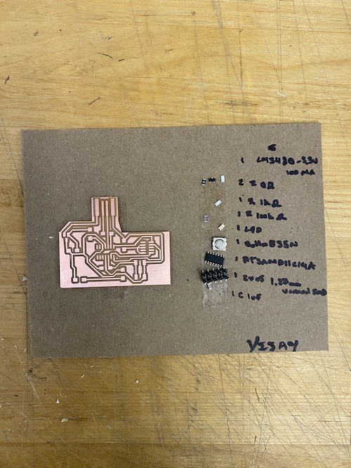
I collected all my components from the lab and prepared them for soldering, but this will have to wait till another day.
I'm looking forward to actually testing my board/future boards and learning to load software onto them. I have a feeling we'll be getting a lot more experience with this in the near future....
As a group we met with Jake earlier in the week and he demonstrated some of the testing equipment -- imparticular how to use the oscilloscope to get a detailed reading of the electrical signal being sent through the board. I'm not entirely sure when we will be using this tool in the future, but it was nice to see it in action.