Electronics Production
make an in-circuit programmer that includes a microcontroller.
PCB Production
This week, I tried to mill and stuff the board. And I also tested it to verify that it works.
Software Operation
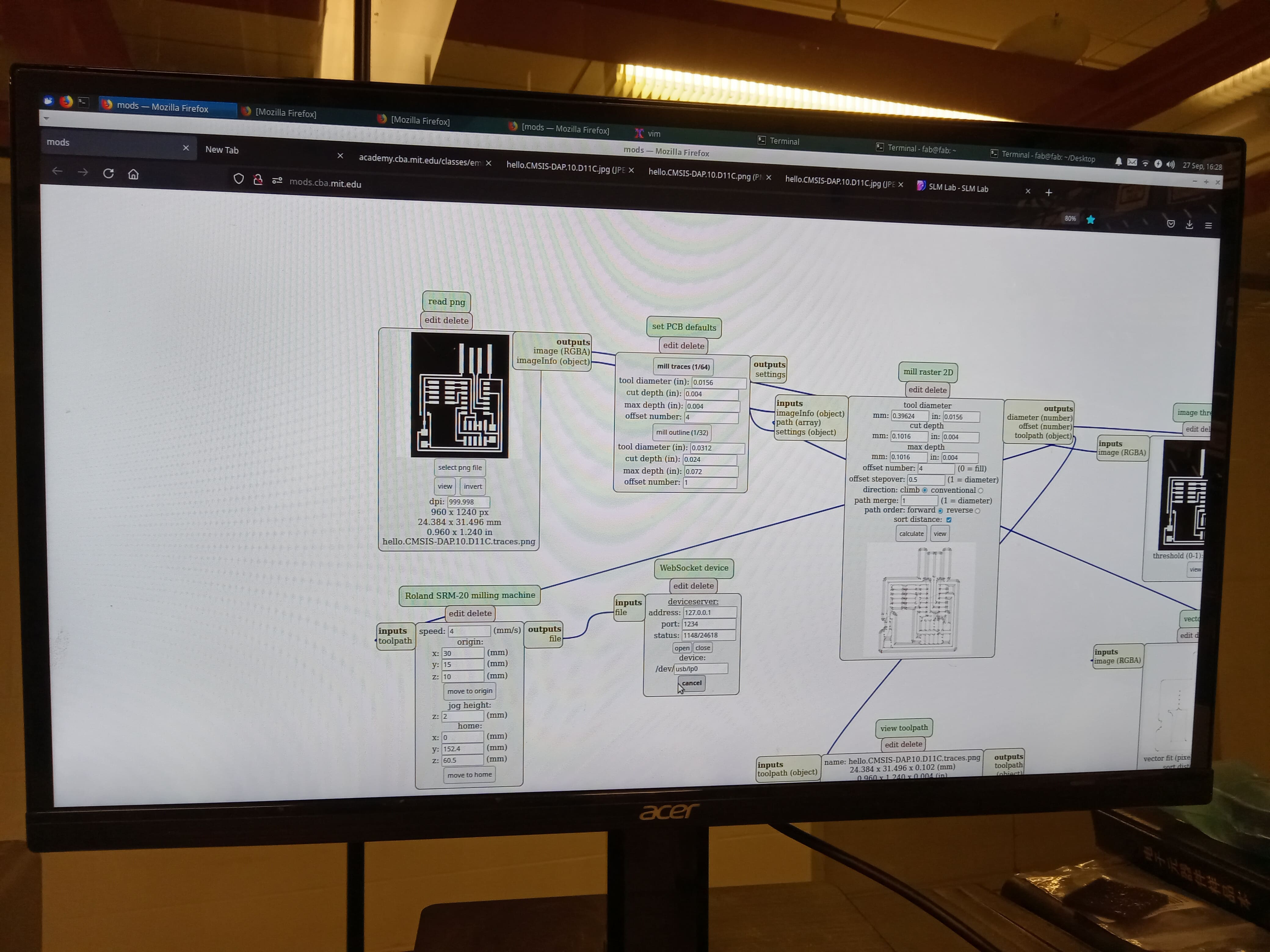
The PCB printing process is controlled by a software. And I followed these steps:
1. Open the machine, use the commands to connect the software with machine.
2. Double-tap a uncutted board on the sacrificial layer, and equip the machine with a end mill.
3. Import the PNG files to start mods, and select "trace" or "outline" and calculate.
4. Adjust the parameters, select "move to origin", and make the end mill bit touch the board.
5. Click "send the file to the device" and the machine will start to work.
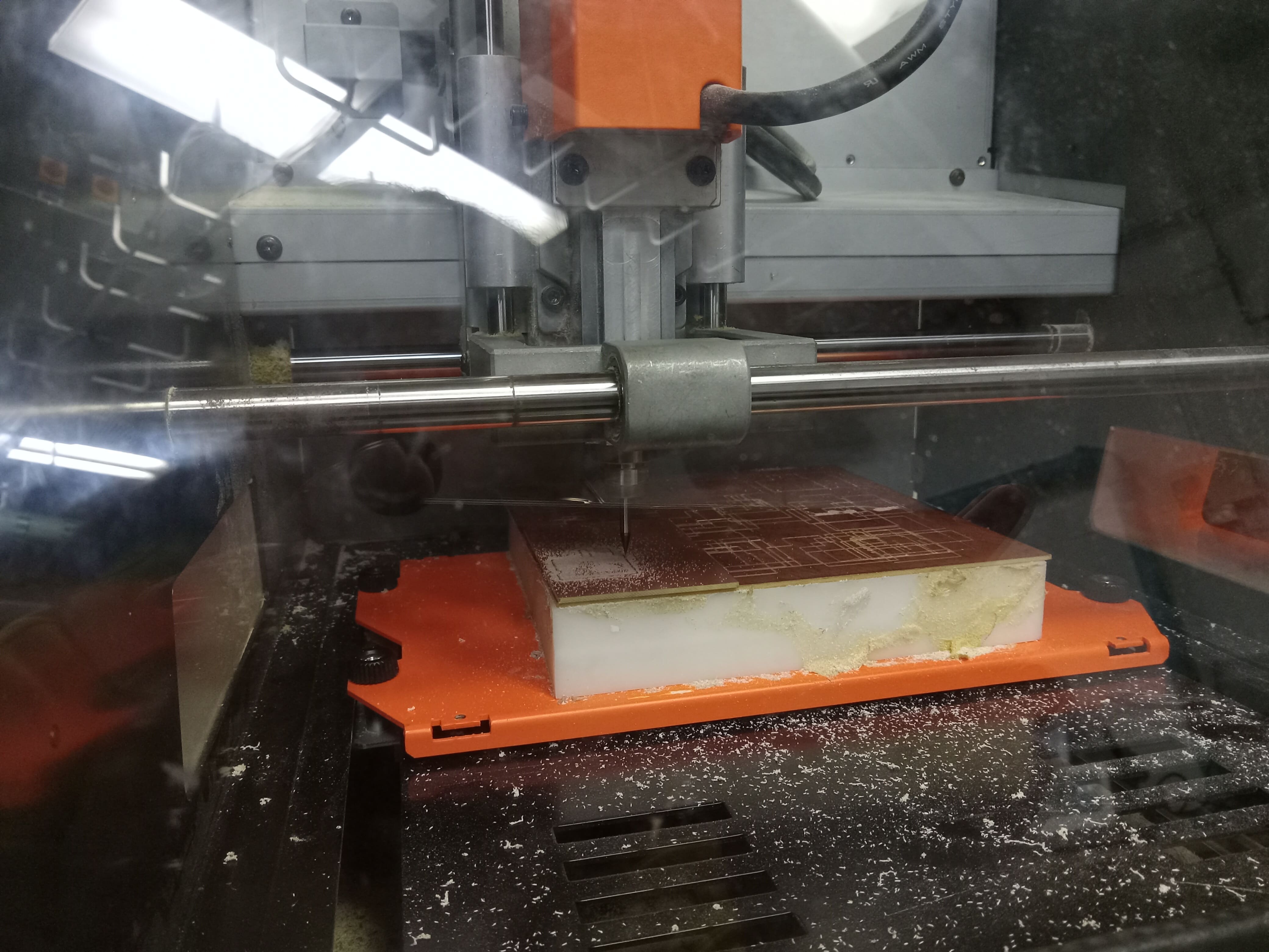
PCB Milling
I used machine to mill the trace first and then the outline. Between these two milling process, I switched the 1/64 end mill to 1/32 end mill.
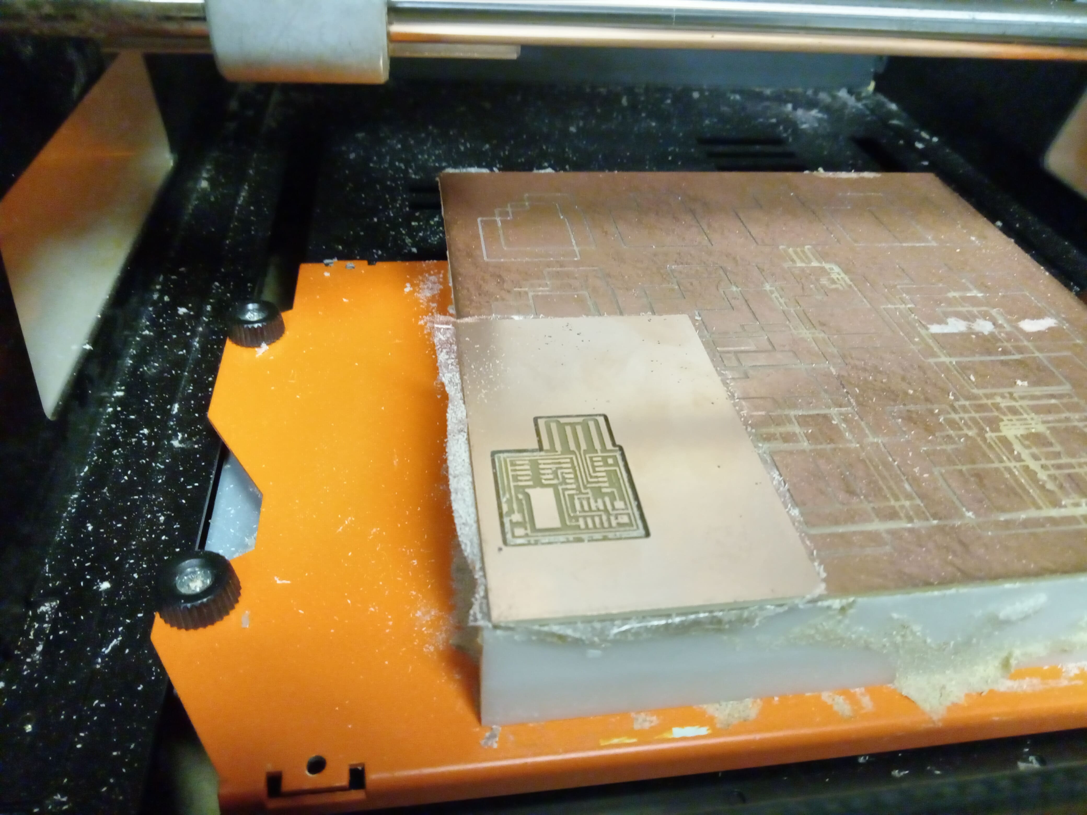
Milled PCB
It is very excited that to see the milled PCB. This is the first time I made the PCB by myself!
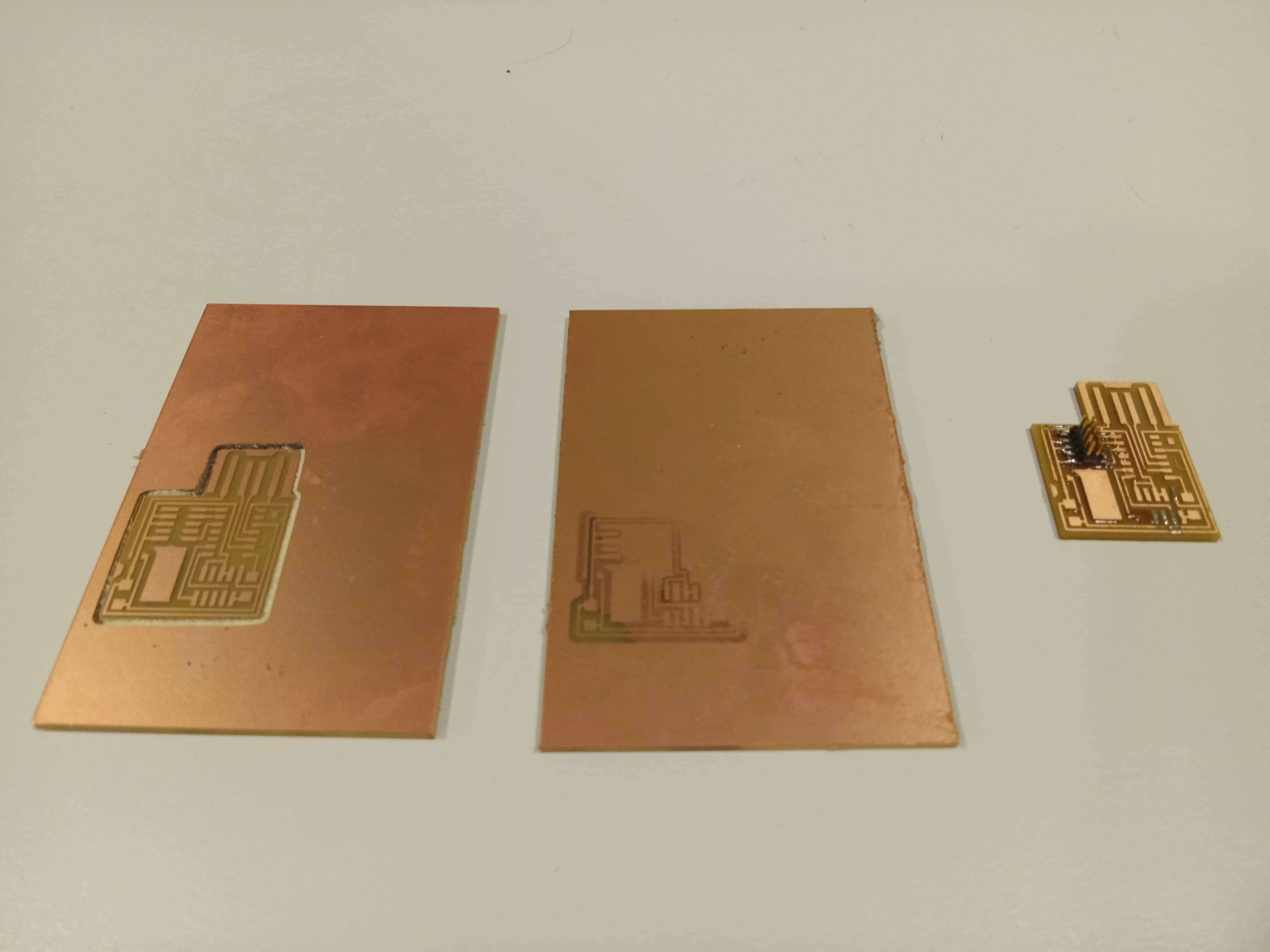
Some Failure Samples
Because it is the first time I try PCB milling and soldering, I met many difficulities.
When I first began to milling, because the board and the underside were not glued tightly enough, in the Mill Outline, the board and the ground as a class began to rotate, and I stopped the machine urgently.
The second time, the trace on the side was not carved because the bottom was not flat enough.
The first time I solded, I applied too much solder and failed to remove it. Instead, I burned the electronic components by trying for too long.
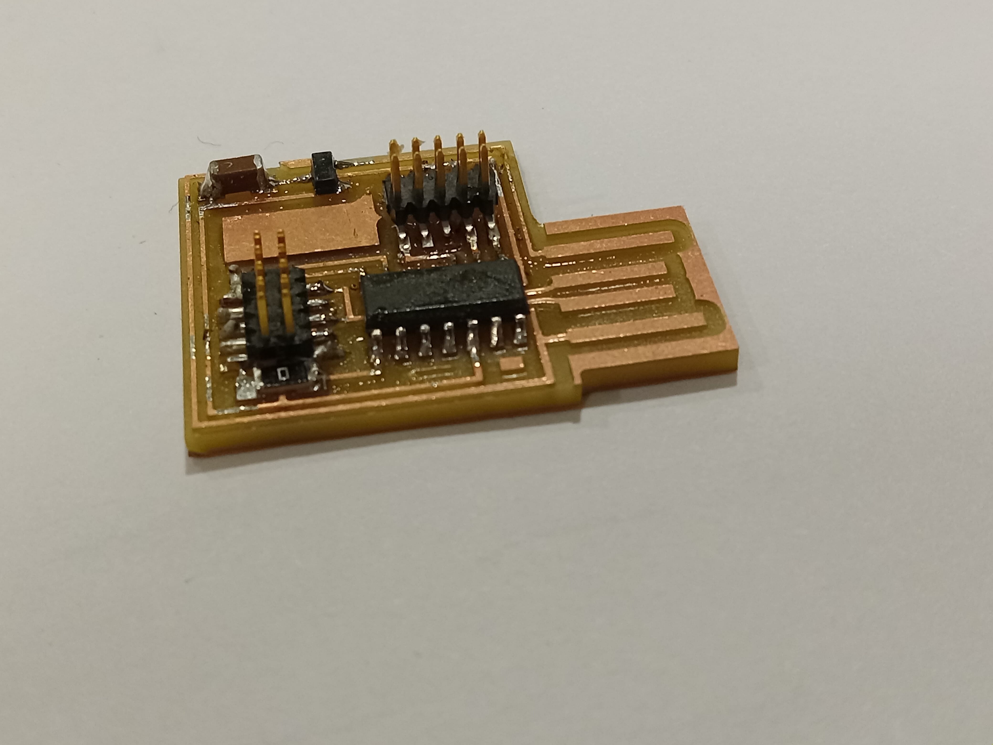
Final PCB
Finally!!! It works. All electronic components (e.g., forward voltage, capacitance and inductance) are solded. And I used the microscope to get a closer and more precise look to check my solded board.
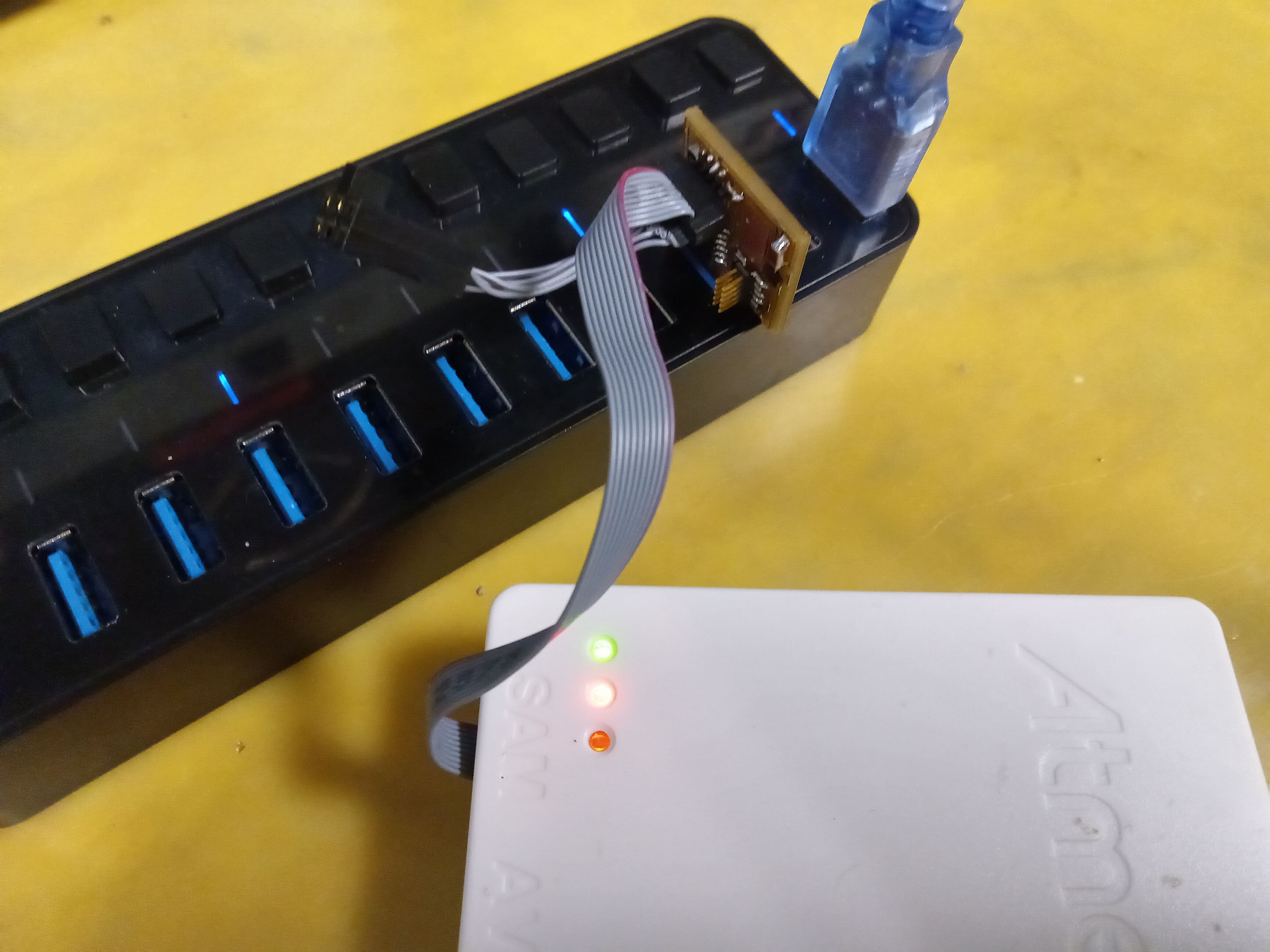
Board Programing
To program the board, I connected the board to the computer.
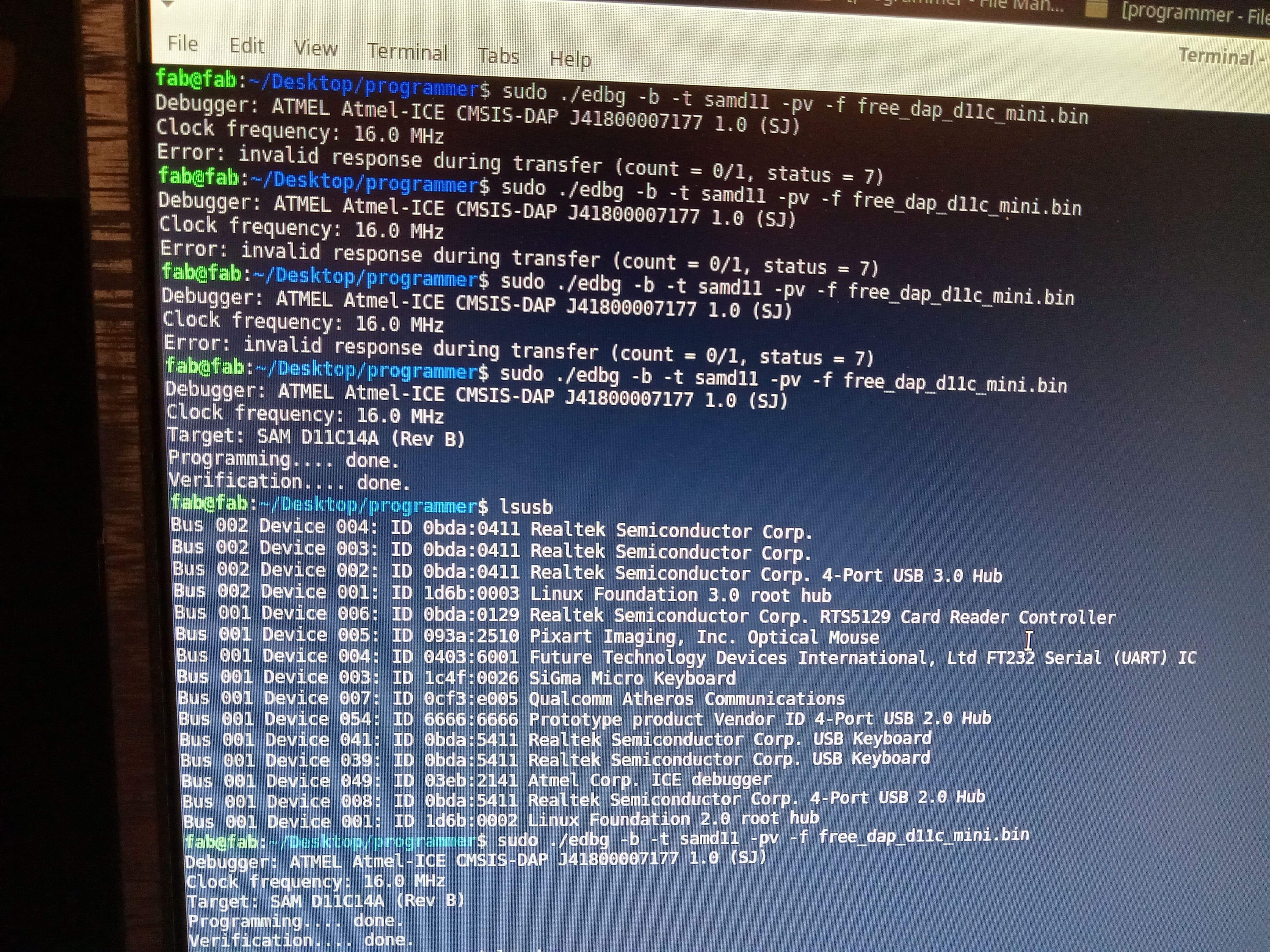
Success
And I runed the command. As shown in the figure, "Verified..." is shown in the screen! I aslo checked the USB suitable. They are look good. I think currently, I can now use this board to program others' board. Happy ending!
The Multi-layer PCB sent to a boarding house
Considering that the PCB I printed by myself is a single-layer circuit, I sent a multi-layer circuit to a boarding house to print. The details of multi-layer PCB can be found in https://fab.cba.mit.edu/classes/MAS.863/CBA/people/Zihan/hw7.html.