Embedded Programming
browse through the data sheet for microcontroller and and program my board to do something.
Introduction
These PCB are designed for Shoes-based foot gesture sensing and interaction. The PCBs were originally designed for the Shoes++ project, which can be found at https://www.detachablesole.com/. The reason why I re-produced all these PCBs is that the old version is left in China, and when I would like to explore the foot interaction further and I found I don't have the hardware now.
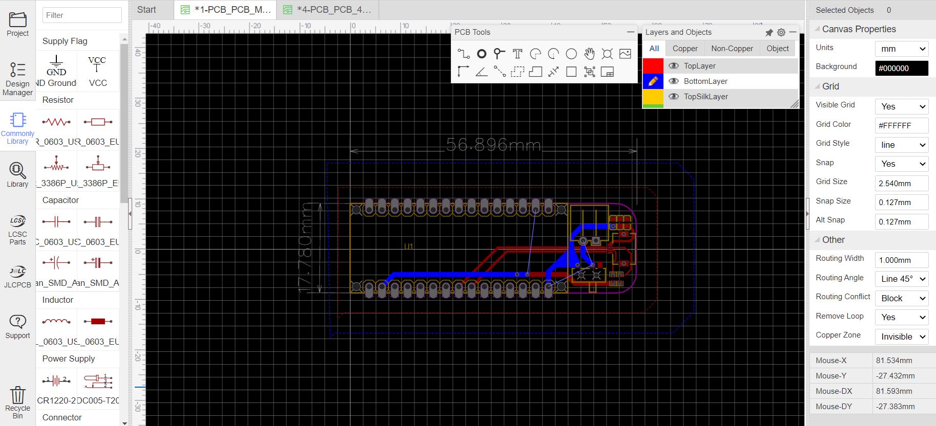
The overall function of this set of PCBs is to use the inertial measurement unit (IMU) to sense foot movement and thus understand the foot gesture and interaction. The whole sensor system includes three IMU nodes (secondary nodes), an Arduino Nano 33 BLE (primary node) and lithium battery. I designed two PCBs here for multi IMUs with a small size. One PCB is the master node to control the following multi-IMUs. The other is the slave node which reduced the size of the PCB to only 1.1 cm by 1.1 cm.
Design and Fabrication Workflow Overview
I designed the PCBs with EasyEDA (https://easyeda.com/). This PCB-making tool is provided by JLCPCB (https://jlcpcb.com/). This is a PCB company in Shenzhen, China, but it provides international service. I used the service from JLCPCB for two years because it is cheap and fast. And this time, I also sent the PCB to this company for printing.
Source File
I uploaded all related files and codes to my GitHub: PCB files: https://github.com/yzihan/SVG-PCB/tree/main/pcb code for the controller: https://github.com/yzihan/Shoes/tree/main/arduino code for data transformation (both versions of using BlueTooth and serial port): https://github.com/yzihan/Shoes/tree/main/data-trans
Master Node
In the sensor network, an open-source electronic prototyping platform (Arduino Nano 33 BLE) with a BLE (nRF52840) module are used as the master node.
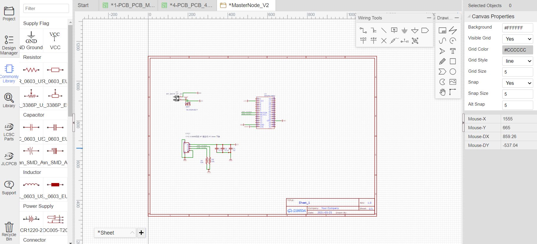
Schematic diagram
Here is the schematic diagram of master node, which has BLE module.
IMU
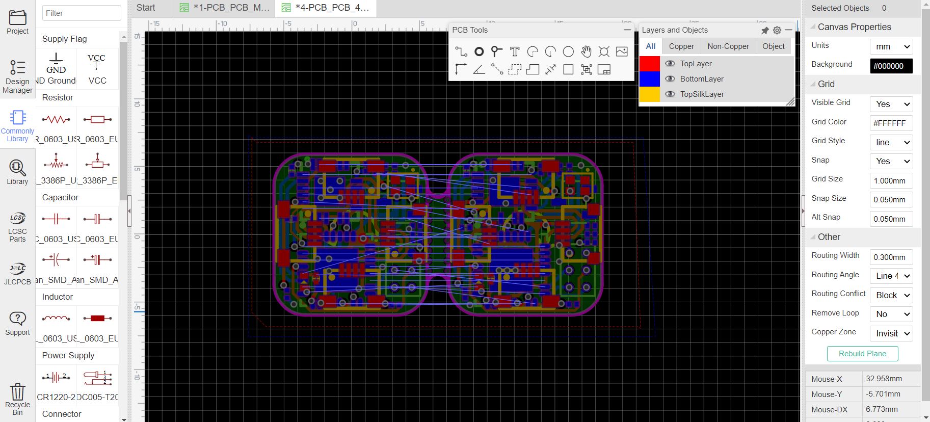
Then I designed and manufactured a modular and compact printed circuit board (PCB) for IMUs, shown in Figure. To reduce the dimensions and weight of the sensor network, I reduced the size of the PCB to only 1.1 cm by 1.1 cm. It is a a 4-layer PCB layout scheme.
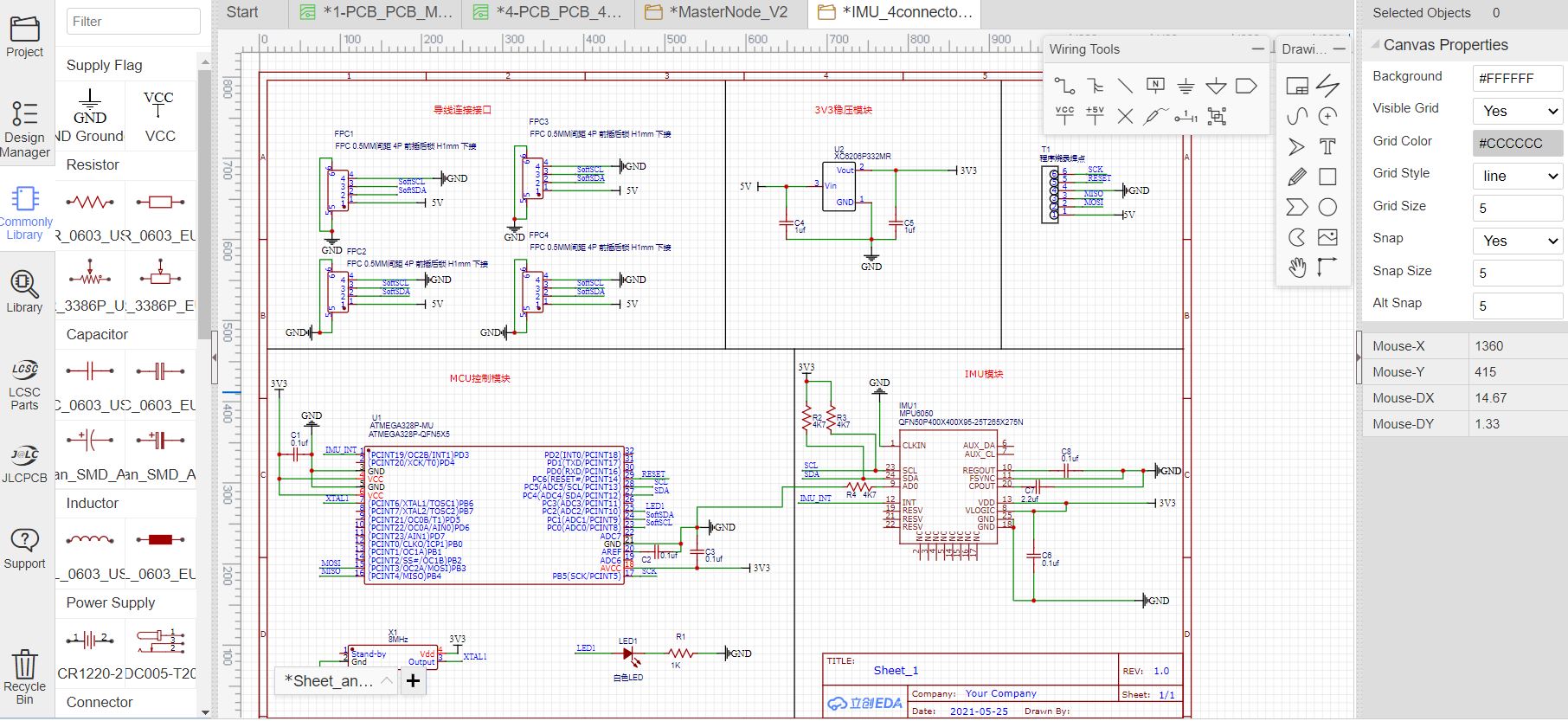
Schematic diagram
As shown in Figure, here is the schematic diagram for IMU node.
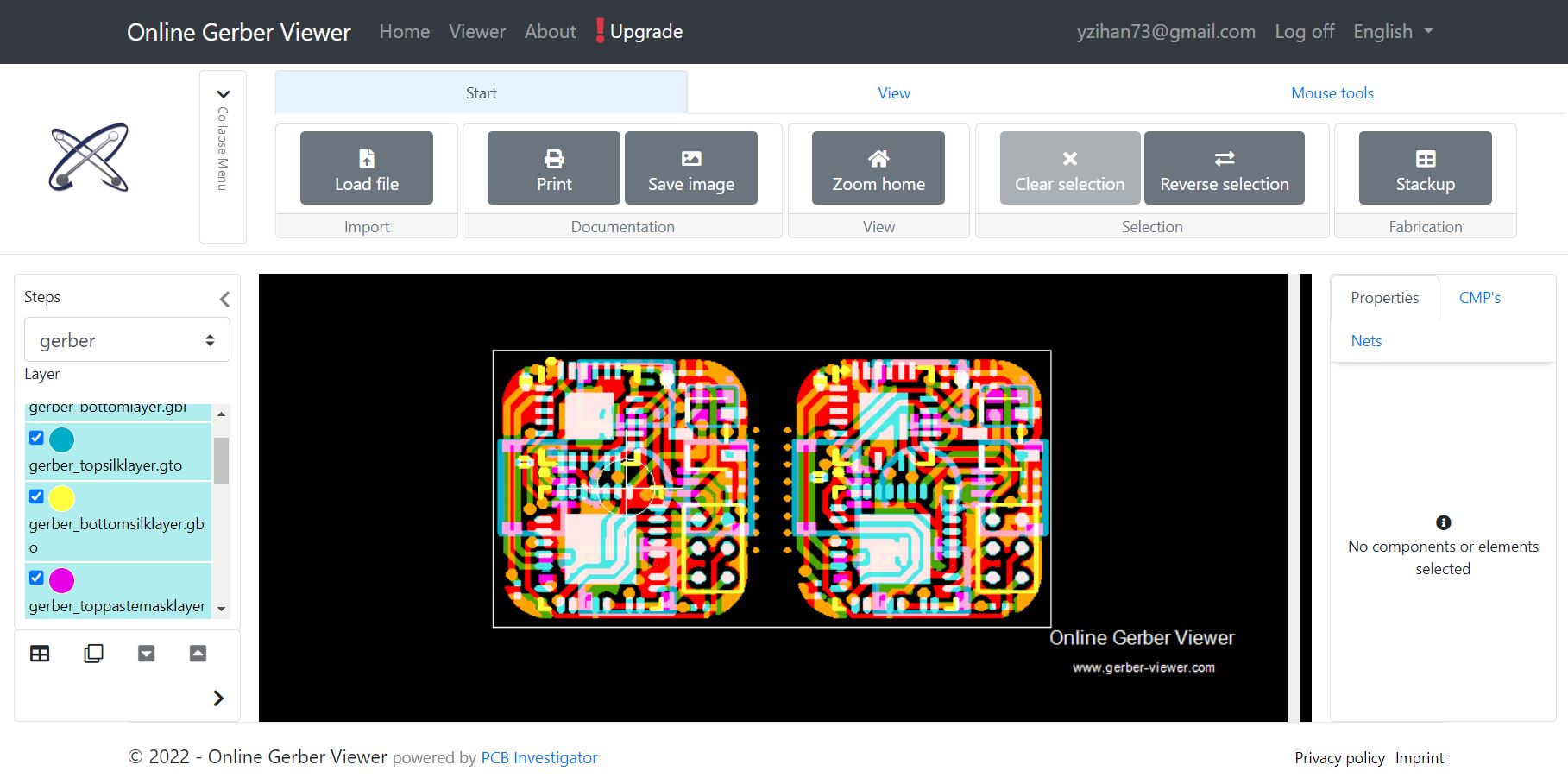
Gerber Viewing
Considering it is a multi-layer structure, I send it to a china factory to print the PCB. Before printing I generated the gerber file by https://www.gerber-viewer.com/.
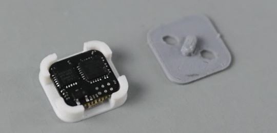
IMU welding
Due to the small size, the IMU is very difficult to weld.
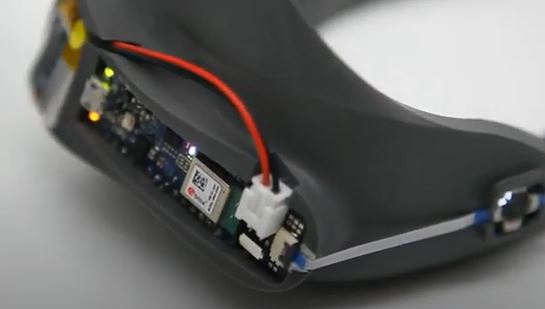
Final Devide
Then I made the final product which can recieve the signals from IMU motion, which shown as figure.
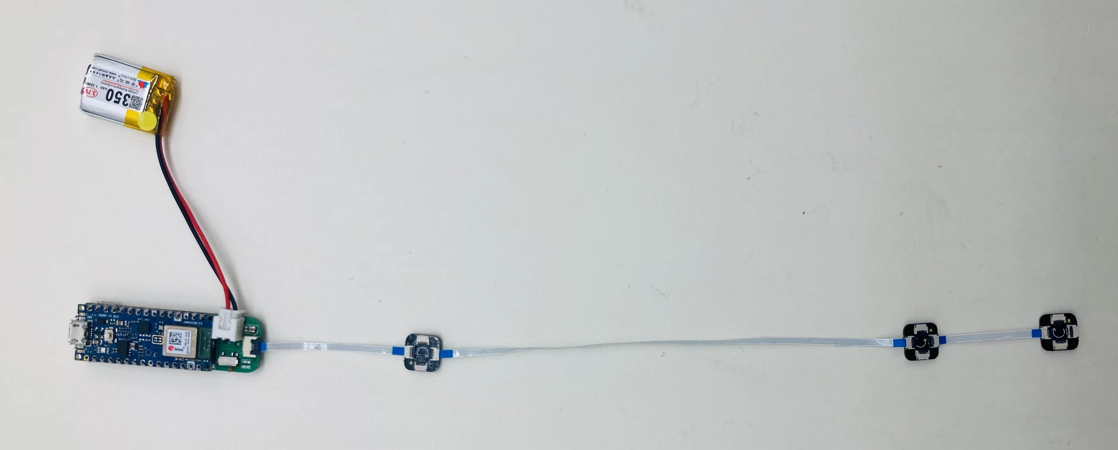
Amplification
These two pictures have larger components and can be seen more clearly.
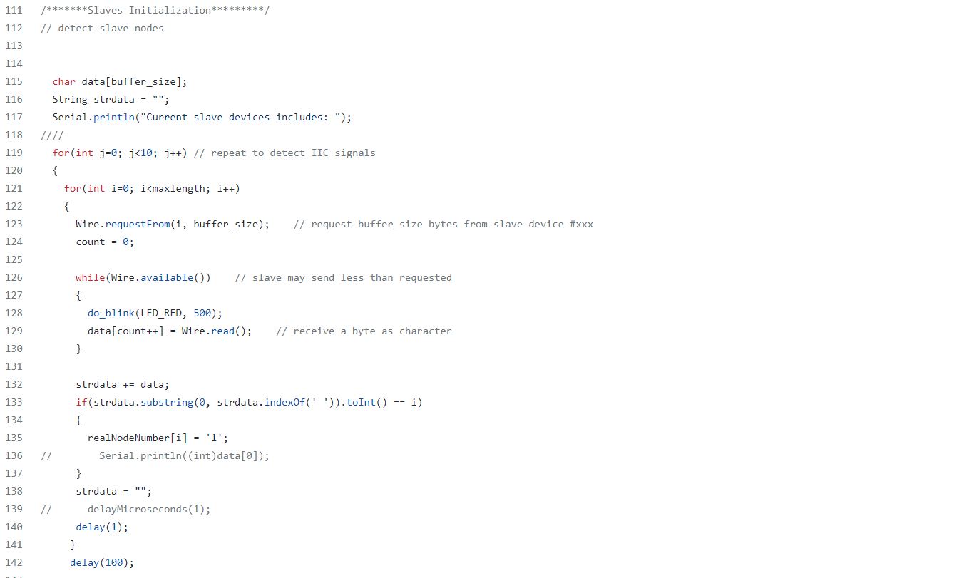
Code for Slave Node Initialization
If slave nodes can be detected, the initalization can be done. And the LED will lighten to enable me know it is ready.
LED Lightening
Then it is simple to make the LED lighten.