Week 6
Group Assignment
A big group of us attended Quentin’s Carvera Training on Thursday. After the training, we downloaded the provided test file and fabricated it using the same flow. Initial struggles included the offset setting, which we had changed towards the end of training, but forgot to change back. Our progress is documented on the section page.
After fixing our problems, we found that the process was able to create all clearances that were .016" or more, but none that were .015" or less. This makes sense, because the end mill is 1/64", which is 0.015625". As for trace widths, down to .008" seemed to work fine.
First attempt
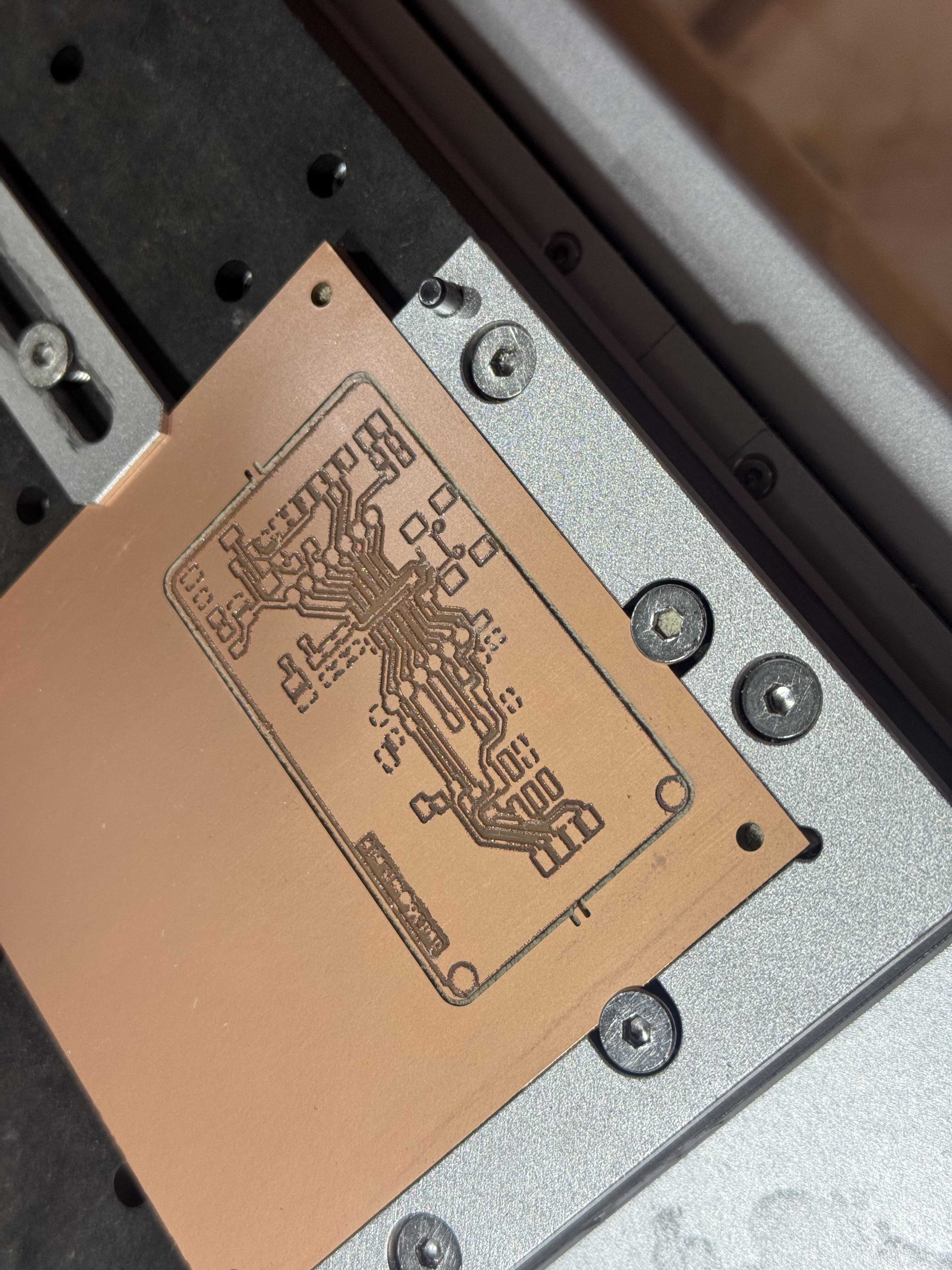
I started by plotting my layout from Week 5. I unfortunately forgot that I had chosen to disregard the DRC warnings inside of the USB Mini-B receptacle footprint. The clearance within the symbol is less than 1/64" by default, so mods (correctly) left the cuts out of the job. I also did not realize that the edge cuts Gerber did not include the drills, so the mounting holes and through-holes were also not part of the job. Furthermore, the edge cuts and copper were misaligned for some reason. Finally, the overall cut was pretty rough. I suspect that the end mill was at the end of its life. The tragic result is shown in Figure 1.
I then returned to KiCad and edited the USB Mini-B receptacle symbol to increase the clearances to 0.4mm by reducing the pad size to 0.4mm (1/64" is exactly 0.396875mm, which is less than 0.4mm). My clearance was already set to 0.4mm, so the board passed DRC completely this time, as expected.
At this point, I unfortunately had to pause my progress in favor of other work.
Second attempt
After completing the Week 8 assignment, I circled back to completing the Week 6 assignment. I made 5 changes to the design based on lessons learned from Week 8:
- I added the mounting holes to the schematic (bcc9d6d)
- I changed the minimum clearance from 0.4mm to 0.44mm and improved the layout to pass DRC with this constraint (including the USB Mini-B receptacle footprint; c028b07)
- I decreased the diameter of the through holes from 1.4mm to 1.0mm and increased the copper diameter to 2.1mm (1f81256)
- I exported the drill files (cc2fd16)
- I increased the clearance on the copper pour to make hand-soldering a little easier (8656d6c)
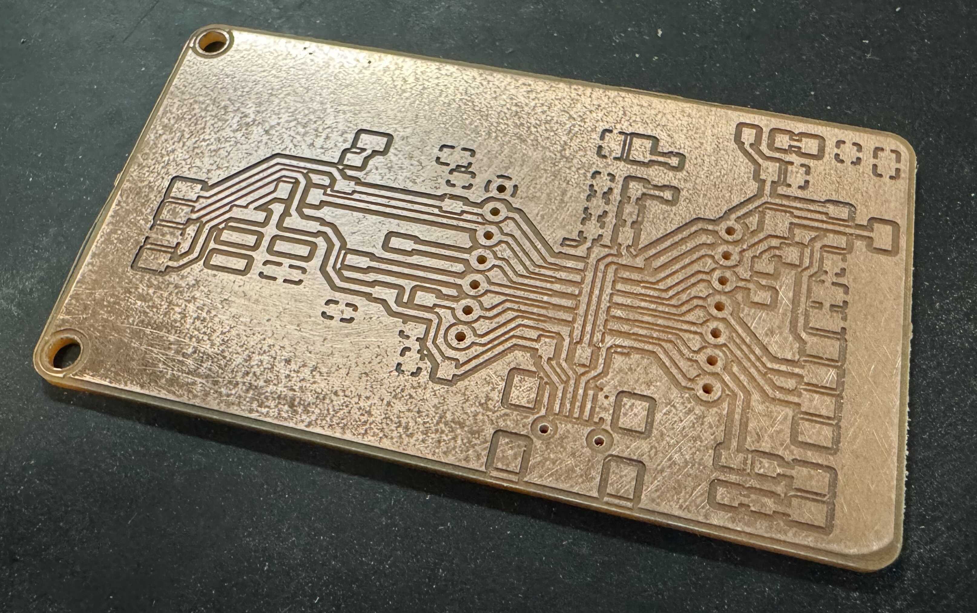
I then re-milled the board on the Carvera and sanded it down. I manually checked for shorts and found none. The result is shown in Figure 2.
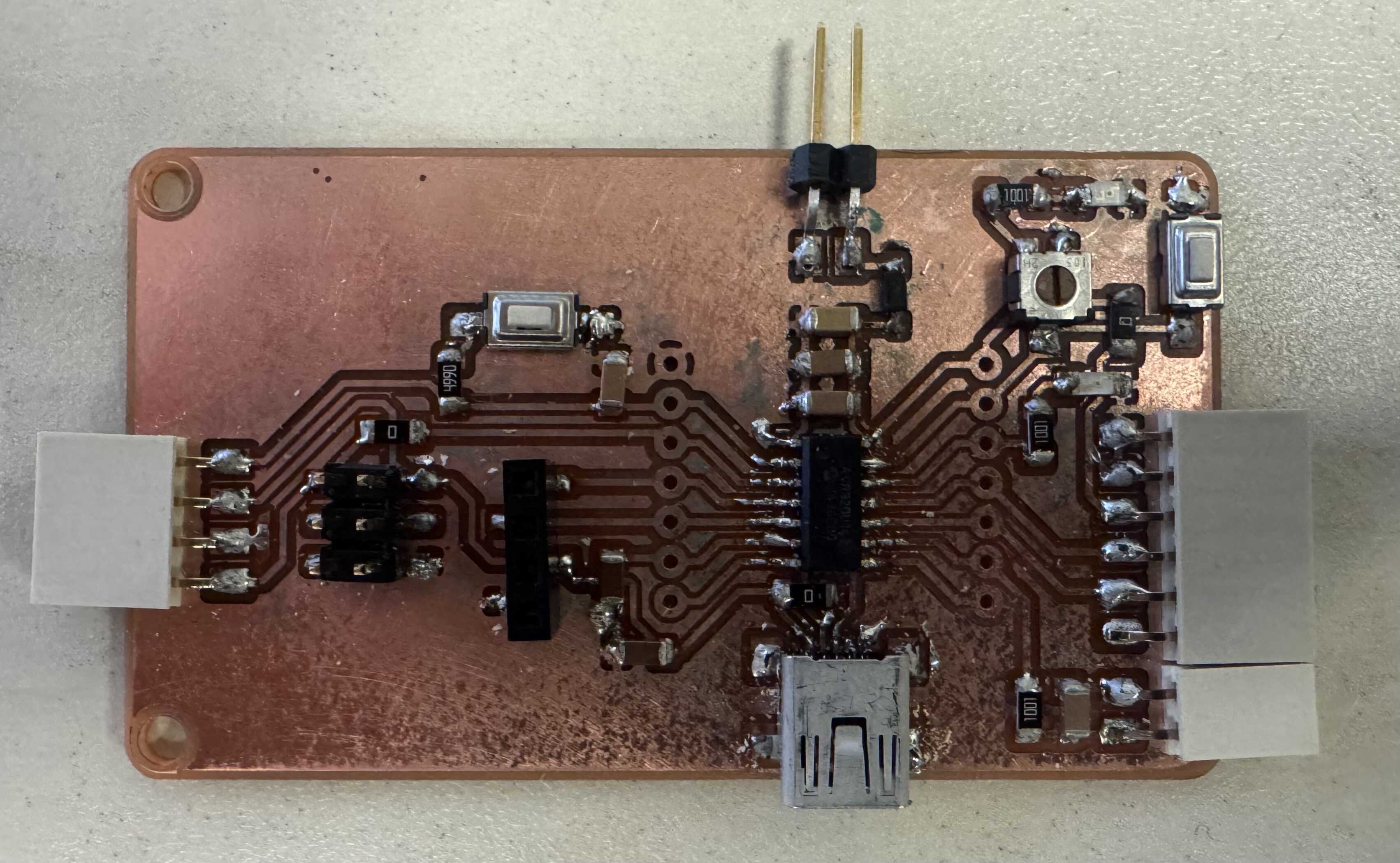
After this, I populated all the components (Figure 3). I used lead-free wire solder for everything.
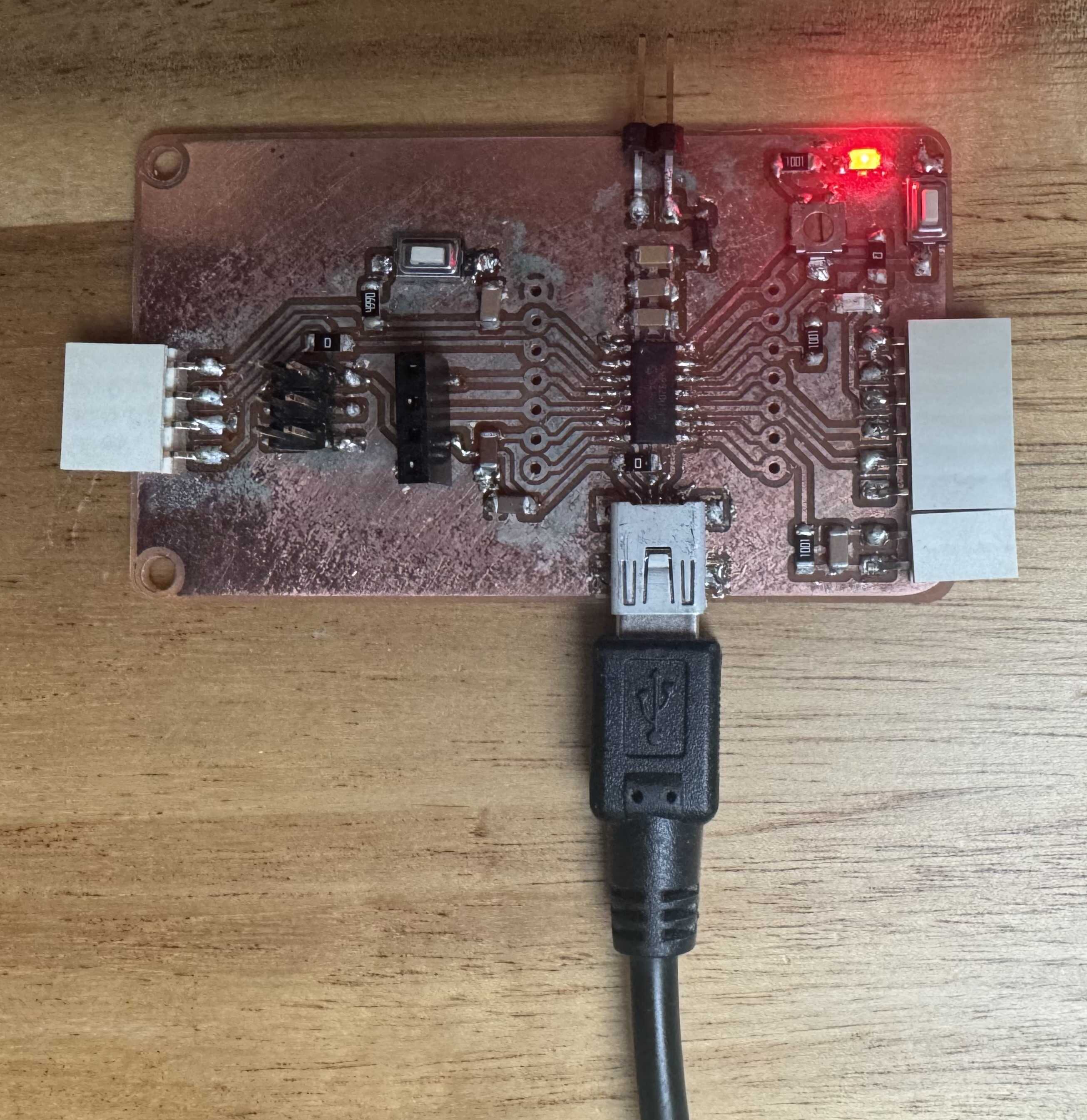
To fully test the board, I need to figure out a way to program it (there is no Arduino core for this chip yet, and the official method has other issues). I am looking forward to figuring this problem out, but decided that it’s out of scope for this week’s assignment. I did verify all nets as I was soldering, and I made sure that the board powers up (Figure 4).


