Week 8
Group Assignment
For the group assignment this week, I met with Ceci, Saetbyeol, Eitan, Rui, Matti and Sophia on Saturday. We probed a SPI front end for a thermocouple. Our work is documented on the section page.
Goal
For this week, I wanted to make a weight scale based on capacitance.
Board Design
I decided against using my board from Weeks 5 and 6,
because I have not figured out a good programming flow for the AVRXXDUXX family yet.
Besides, as documented in Week 6, I had not yet fabricated that board anyway.
Instead, I decided to use the ATSAMD21E18A because 1) it has built-in Peripheral Touch Controllers (PTCs)
2) we have it in stock and 3) I have already seen capacitive touch work on it on the QPAD21.
I called the board the Mini QPAD because that’s what it is
(I even ended up with the same output device, because the OLED is the best thing for my scale).
The only differences are 1) that I decided against adding USB, because I don’t need it
and 2) that I needed the capacitance to be measured off-board, so I added connectors instead.
I used the SM99S01VBNN05G7 connectors from the inventory
(which proved to be the most difficult part of fabrication).
The footprint is nice and large, which allowed for initial testing of the PTCs directly on-board.
I added a connection for Y0 and for X0,
so that I can test mutual capacitance as well.
Finally, I added a 3v3 regulator so that I can run the board off batteries.
I used the same connectors for power as well.
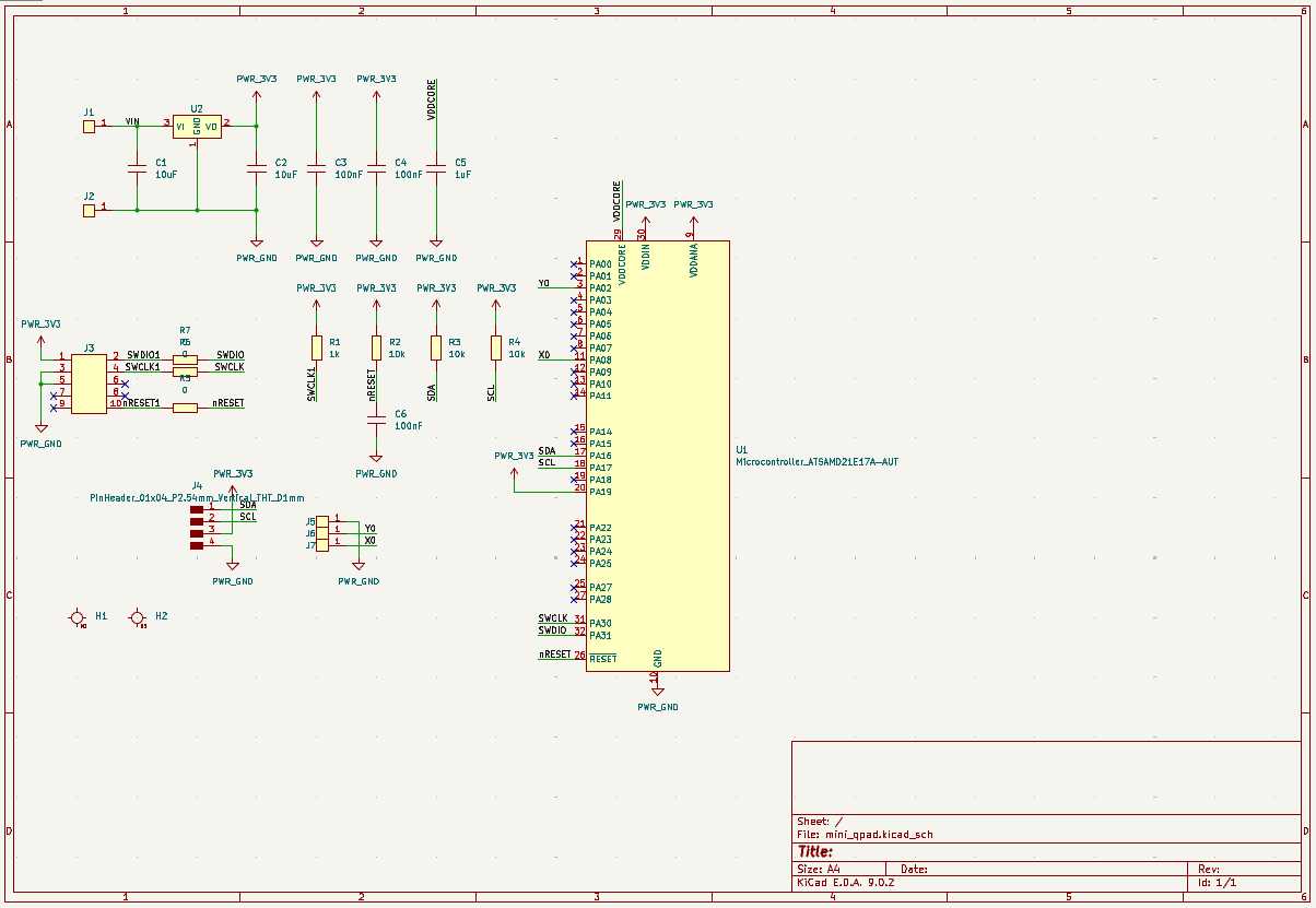
The final schematic is shown below:
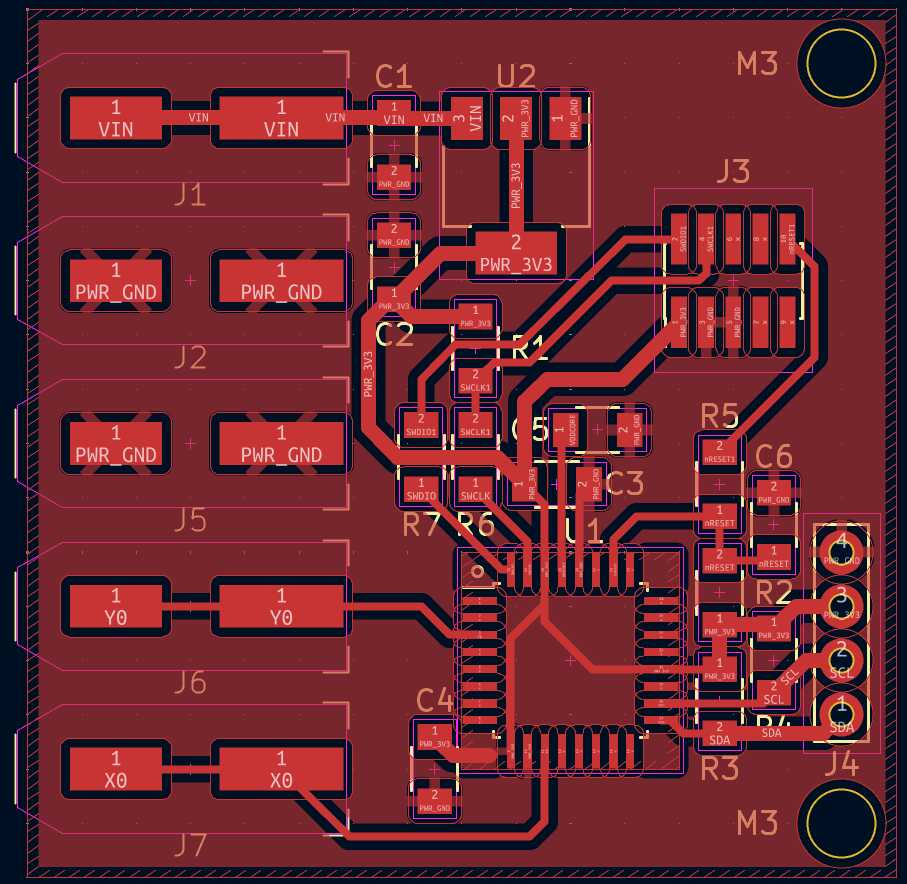
The final layout is shown below:
The source is here: https://gitlab.cba.mit.edu/dimitar/kitchen-sink/-/tree/main/mini_qpad
Board Fabrication
At this point, I had not yet gone back to finish my Week 6 assignment, so a lot of the fabrication learning happened this week.
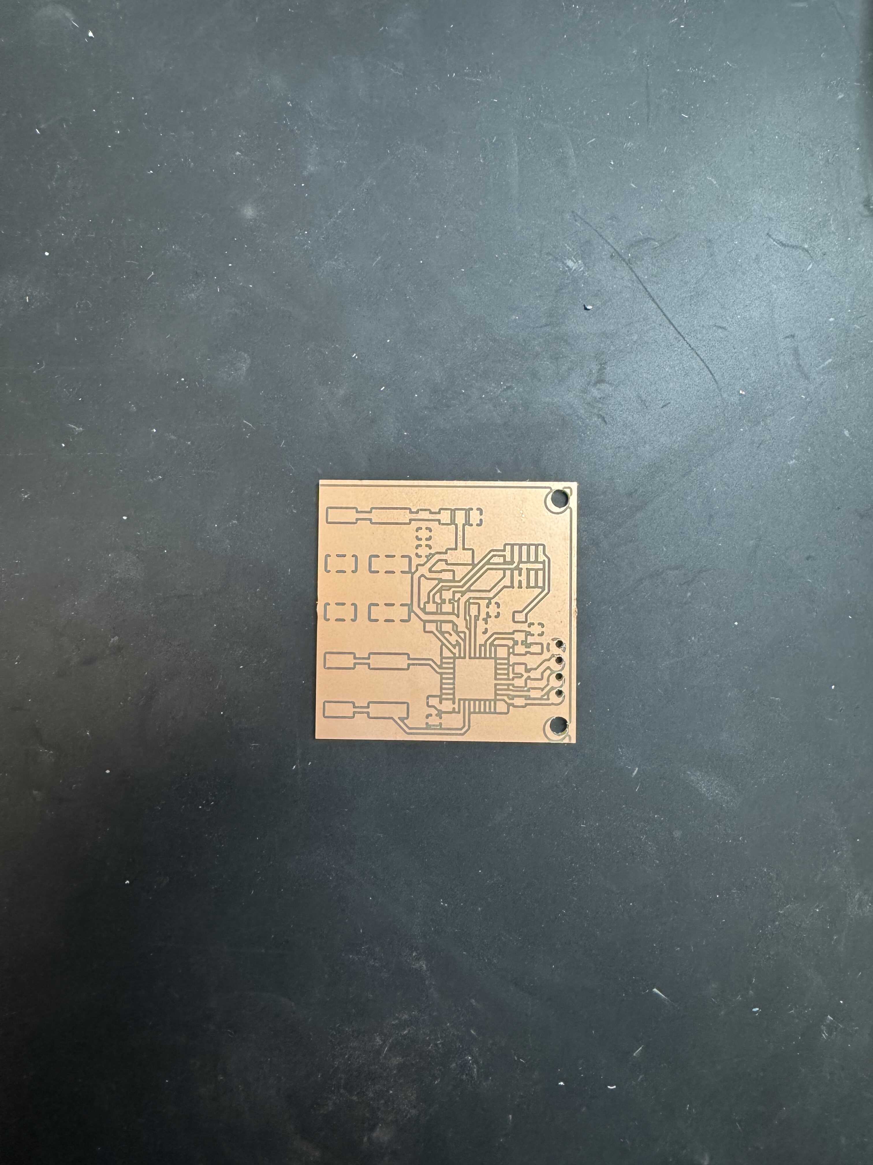
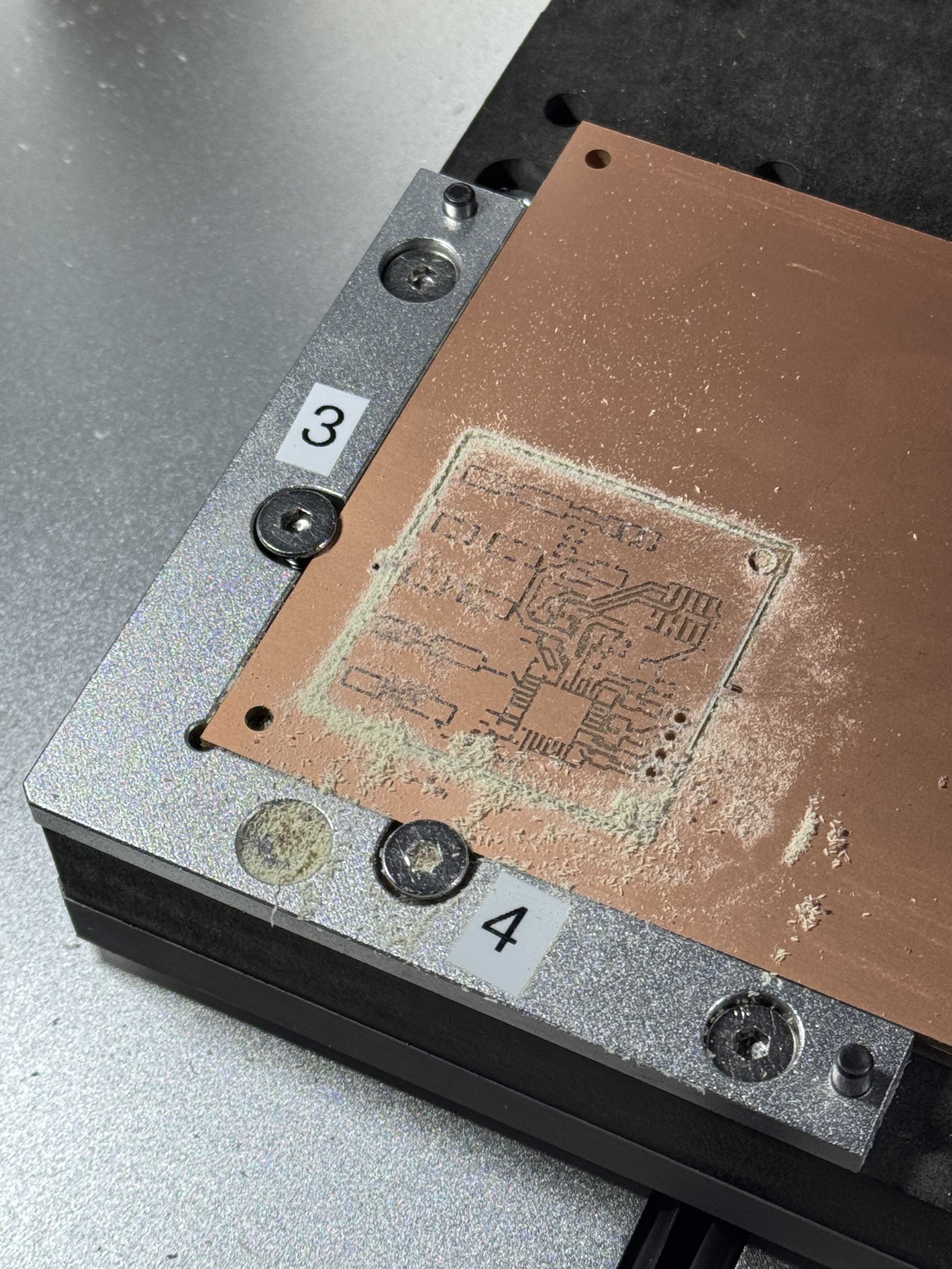
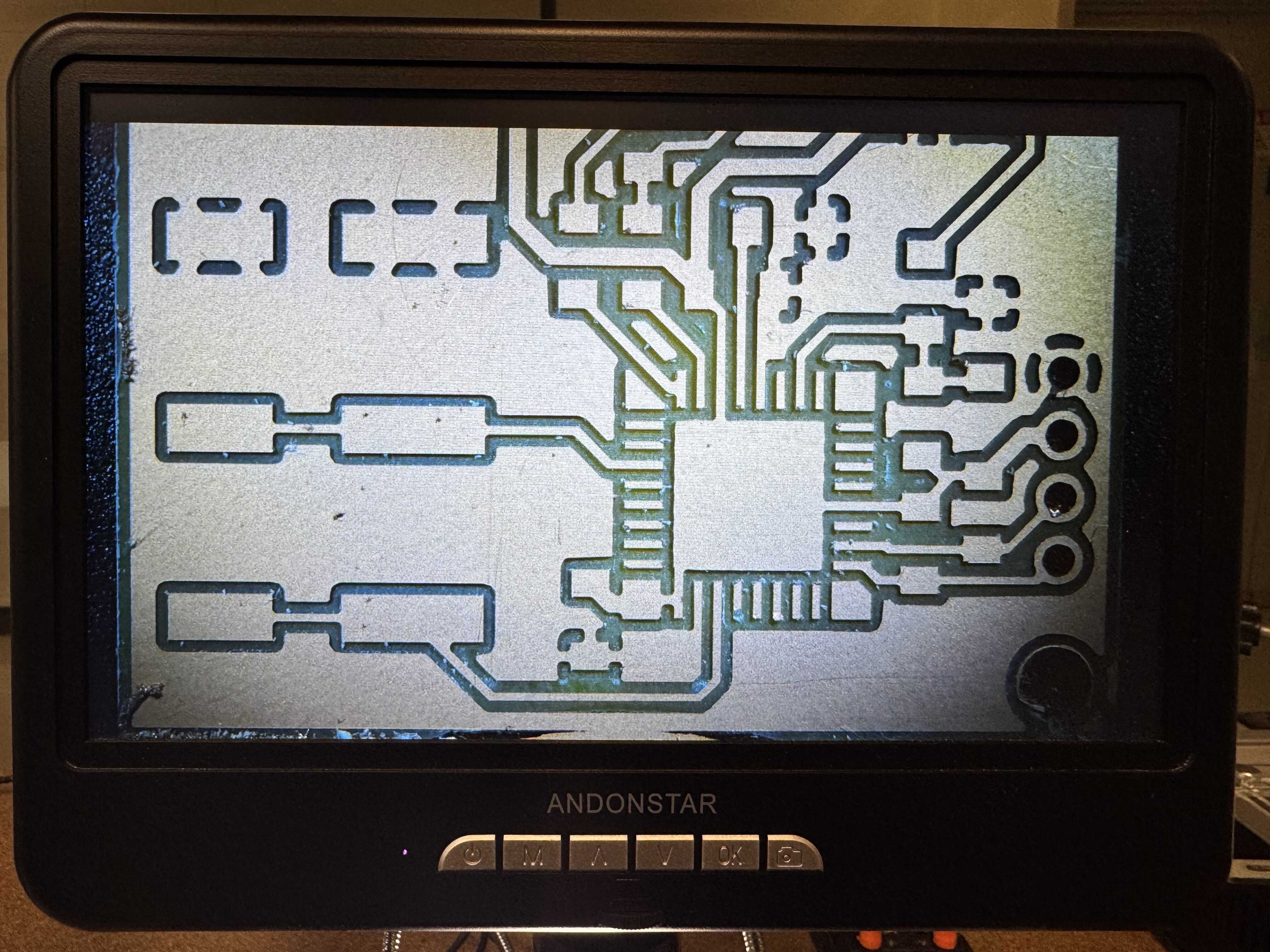
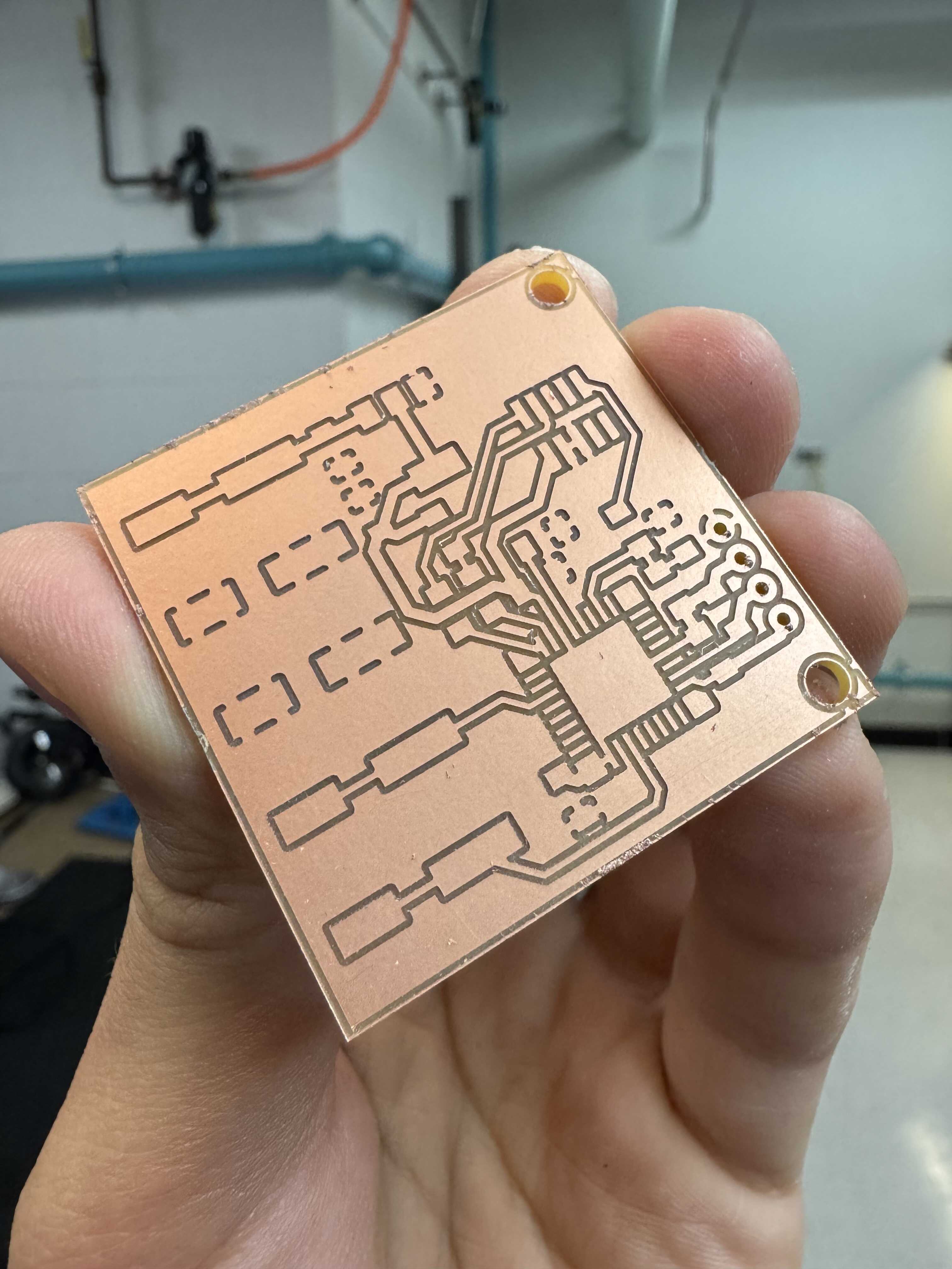
I had already learned in Week 6 to generate and drag the PTH drill file in with the Edge Cuts file, so I didn’t make that mistake again. I had also already learned my lesson about clearances within footprints, so I edited the ATSAMD21’s TQFP footprint and changed the pad widths to 0.4mm, making the clearances 0.4mm as well. When I went to fabricate the board, Krištof was next to me and noticed that despite my 0.4mm DRC passing, the cut path was missing sections. We increased the DPI on the image generation to 2000 and decreased the tool size in mods from 0.4mm to 0.38mm. I also manually set the DPI in mods, because the auto-detected DPI was a little lower than 2000. All three of these steps together fixed the problem, and I fabbed the board successfully:
The edges were much smoother than my previous board, indicating that it likely was a bad end mill the first time. I forgot to look into the alignment issue, so the edge cuts, through-holes and mounting holes were again misaligned.
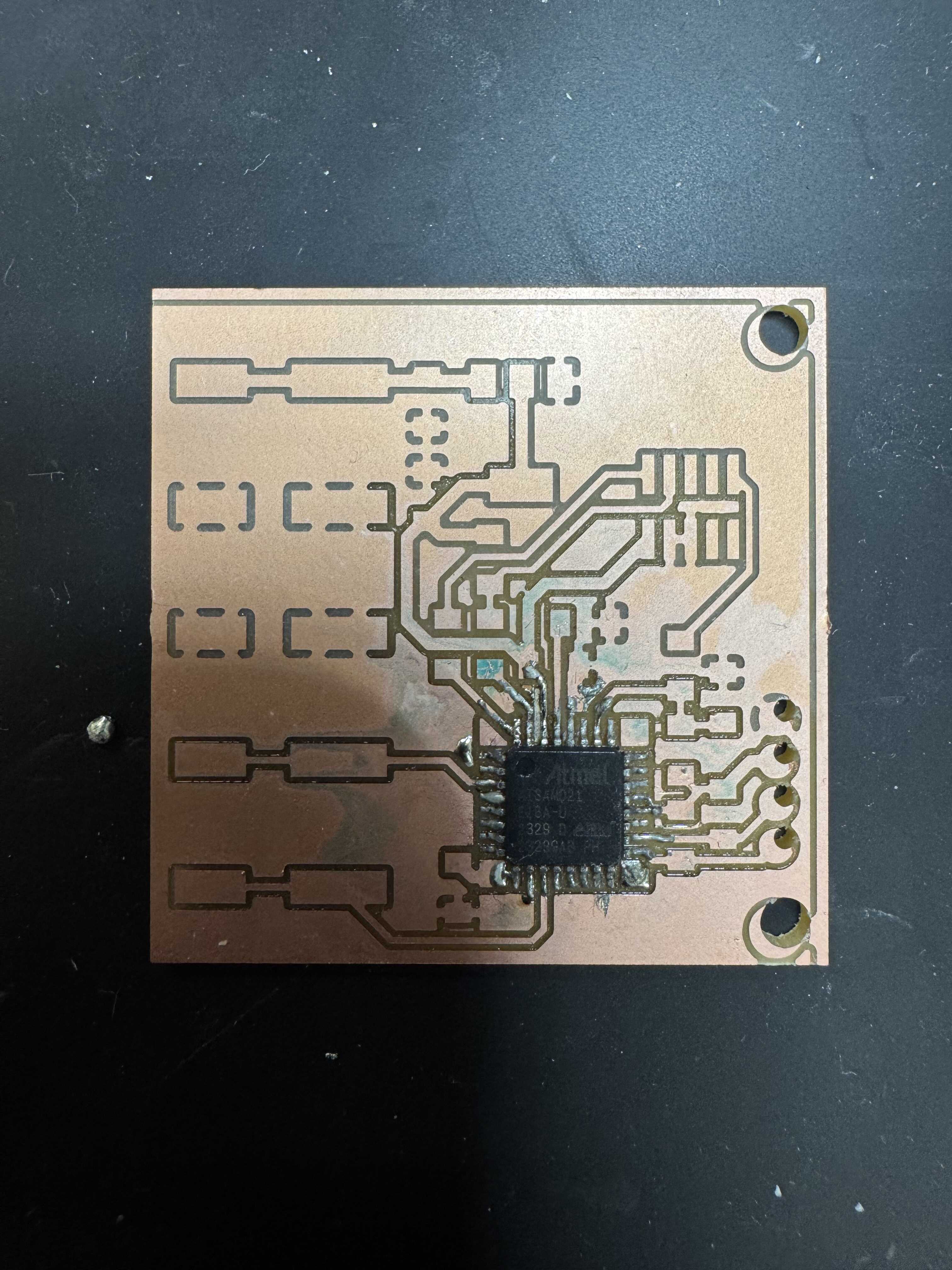
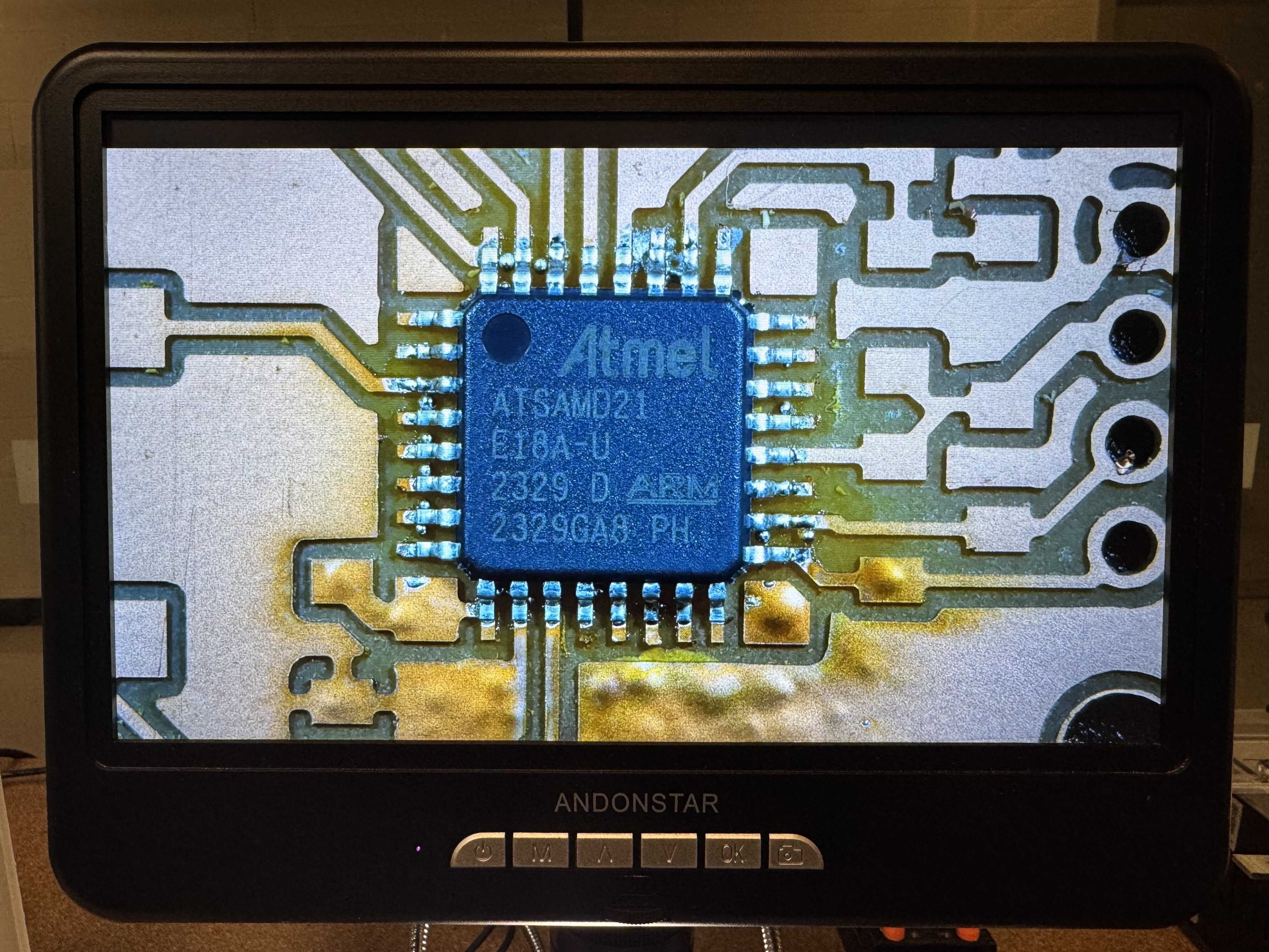
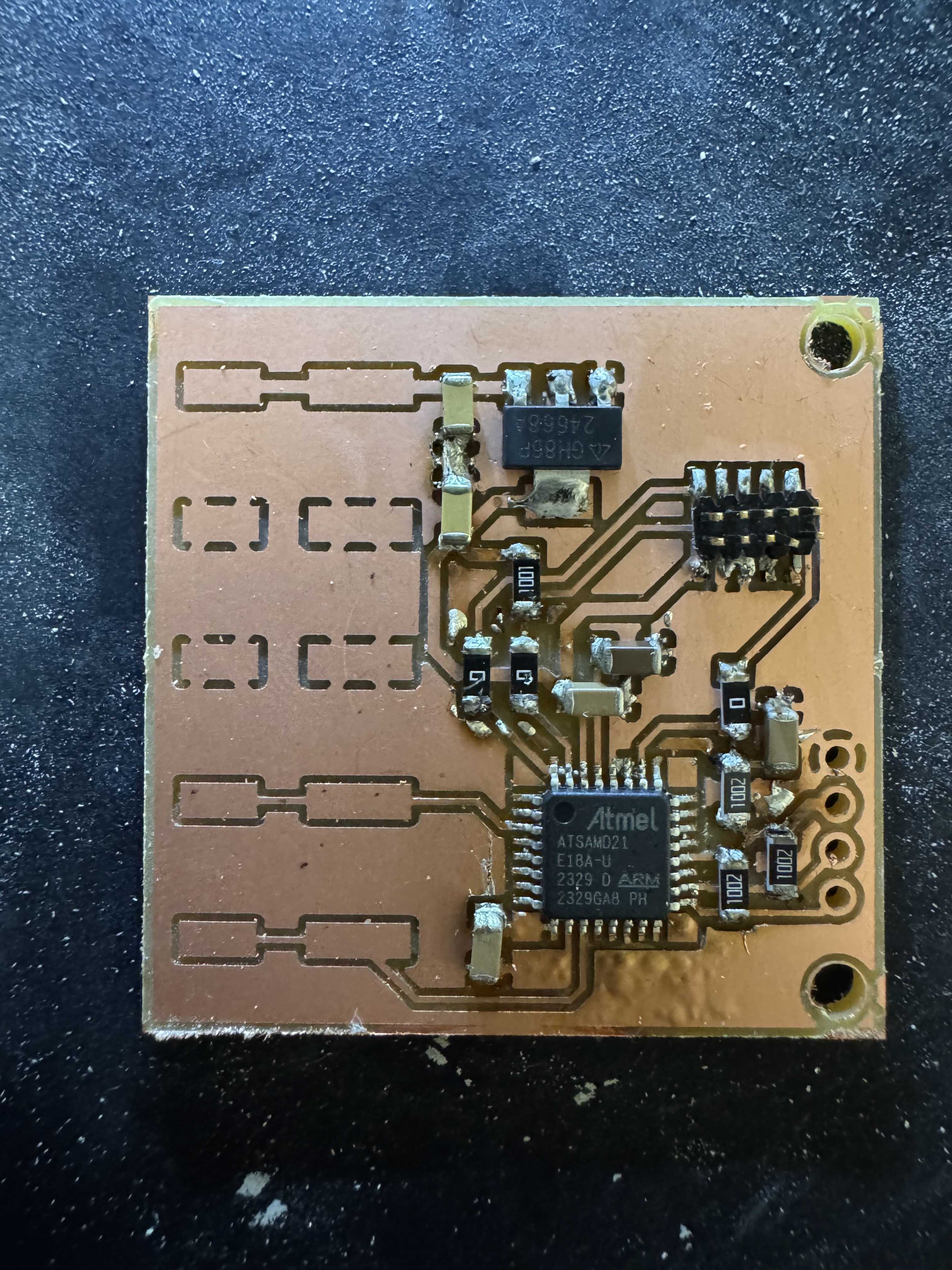
I started by soldering on the microcontroller using wire solder, which went about as smoothly as it always goes for me. But, all the connections were correct:
The rest of the SMD components were no problem. I hooked the board up to a power supply using clips, programmed the chip using Quentin’s programmer, and tested the capacitive touch successfully (see the Software section below).
Then, I went back to do the wire terminals. The pads are underneath the plastic, so wire-soldering is difficult. However, I was using one-sided FR1, so I did not want to reflow from the bottom, either. I briefly tried hot air from the top, but I found that the plastic melted at about the same temperature that the paste reflowed. So, I went back to wire soldering, and it did not go well.
Finally, I tried to salvage the situation using hot air, which spelled the end of this board.
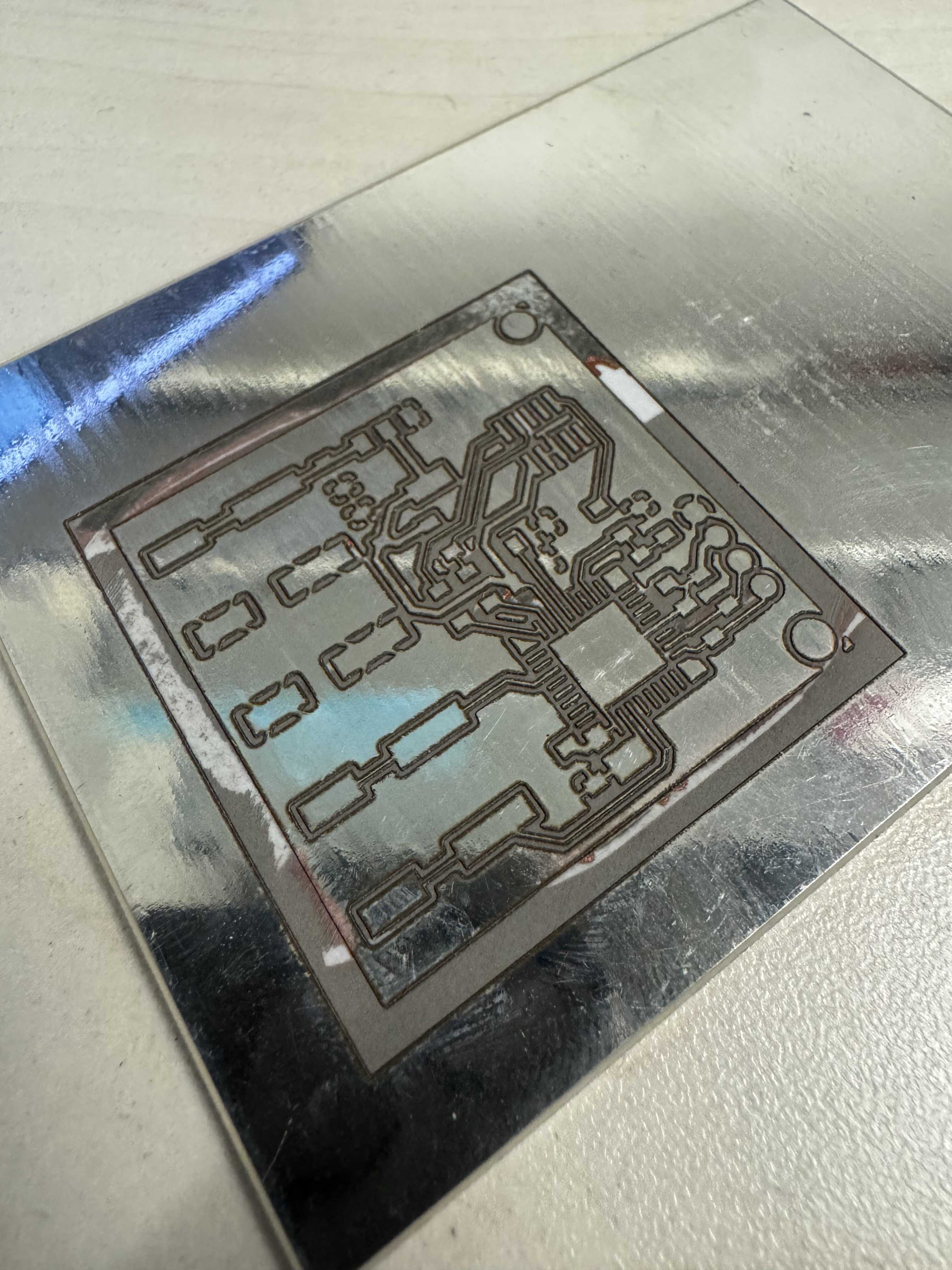
Next, Alan suggested we try an aluminum board on the laser to help with the reflow.
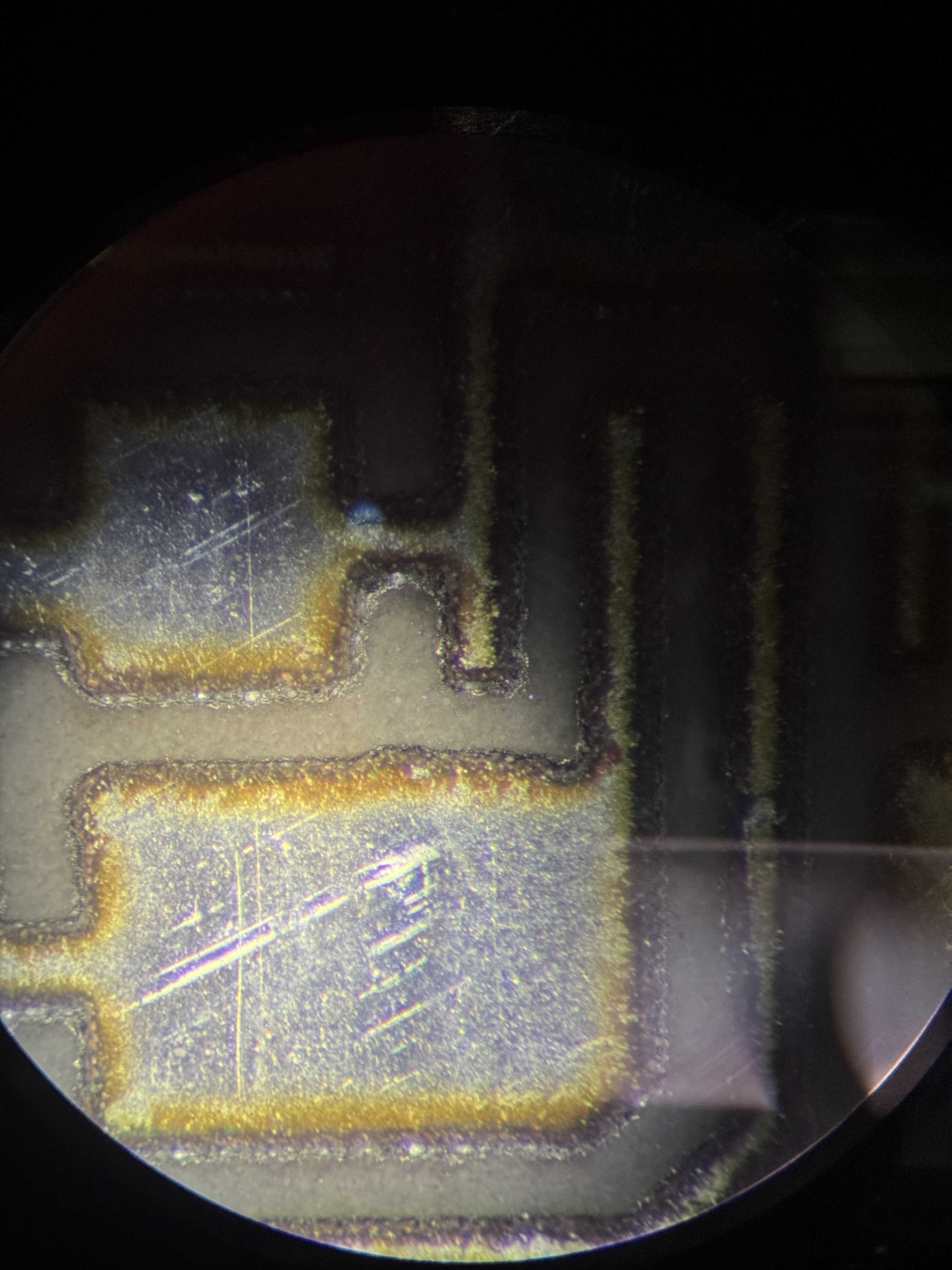
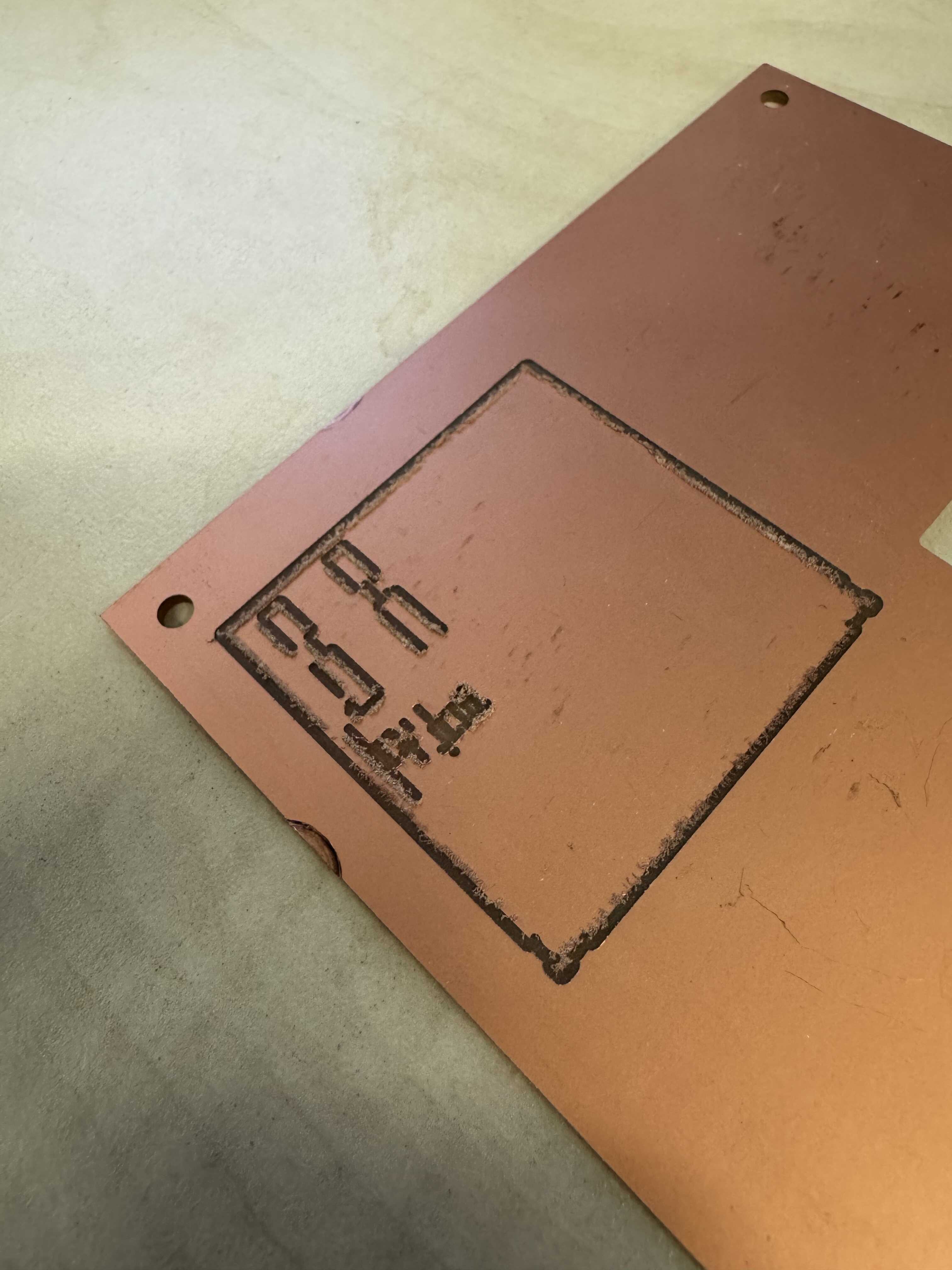
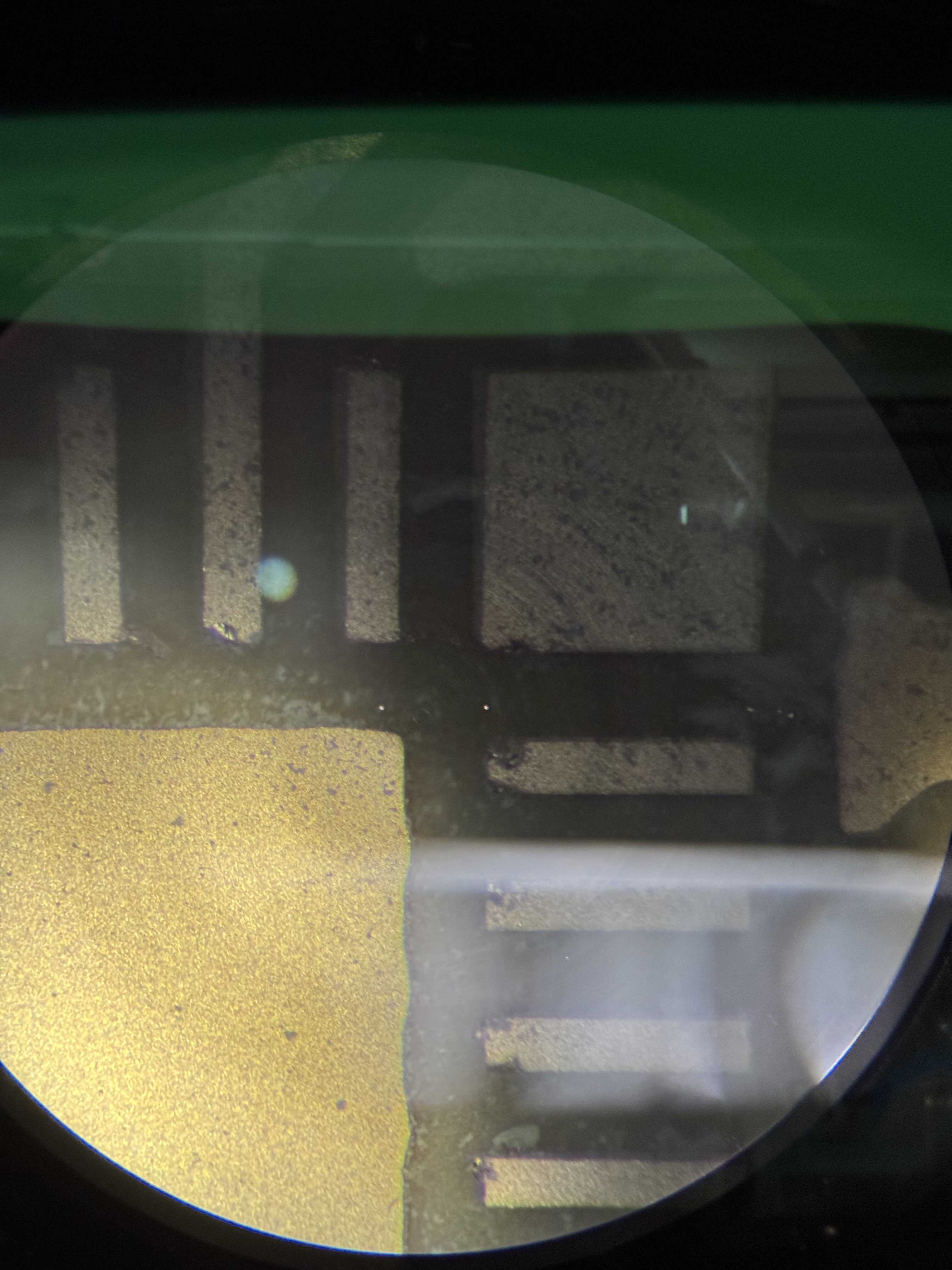
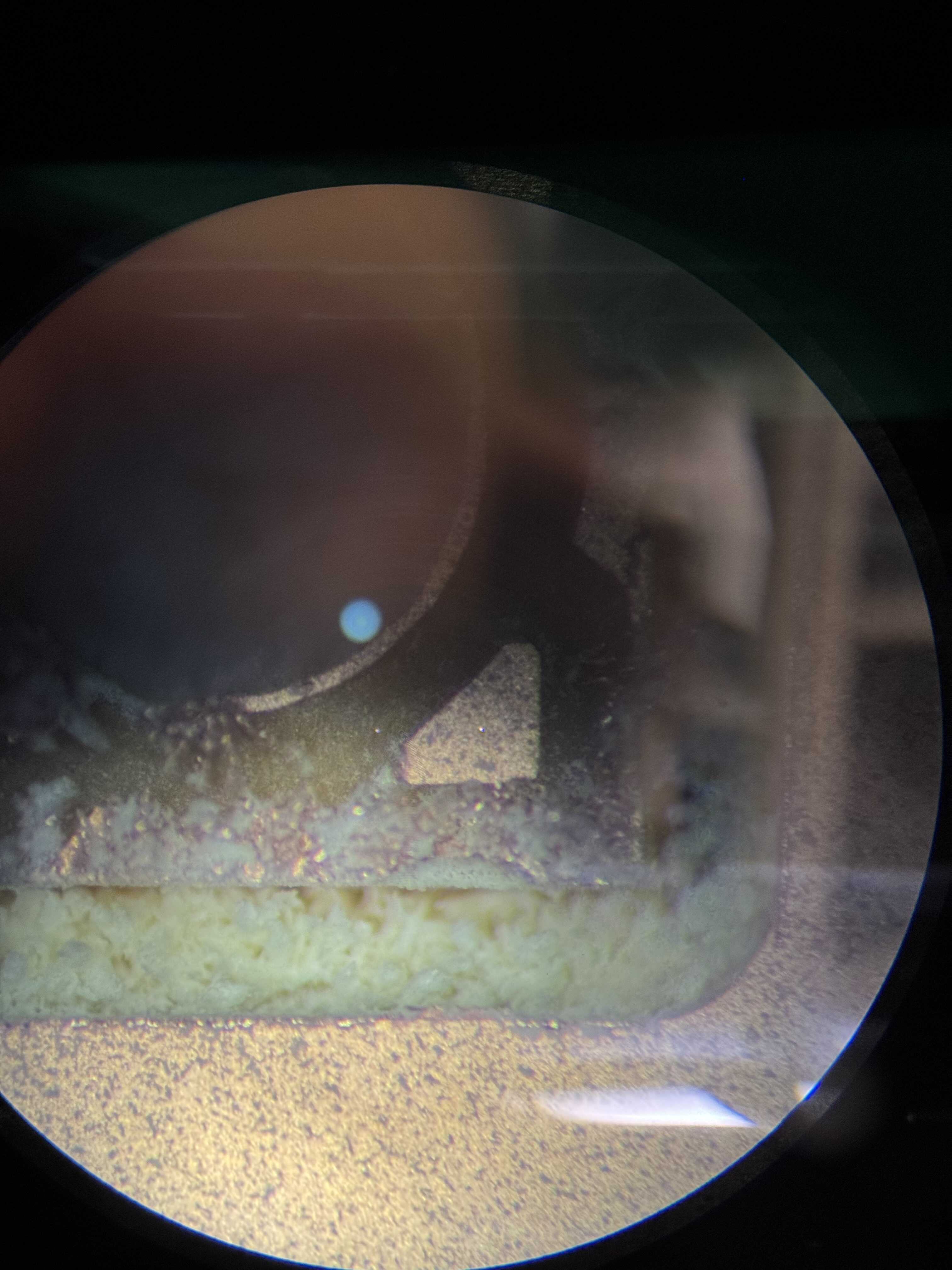
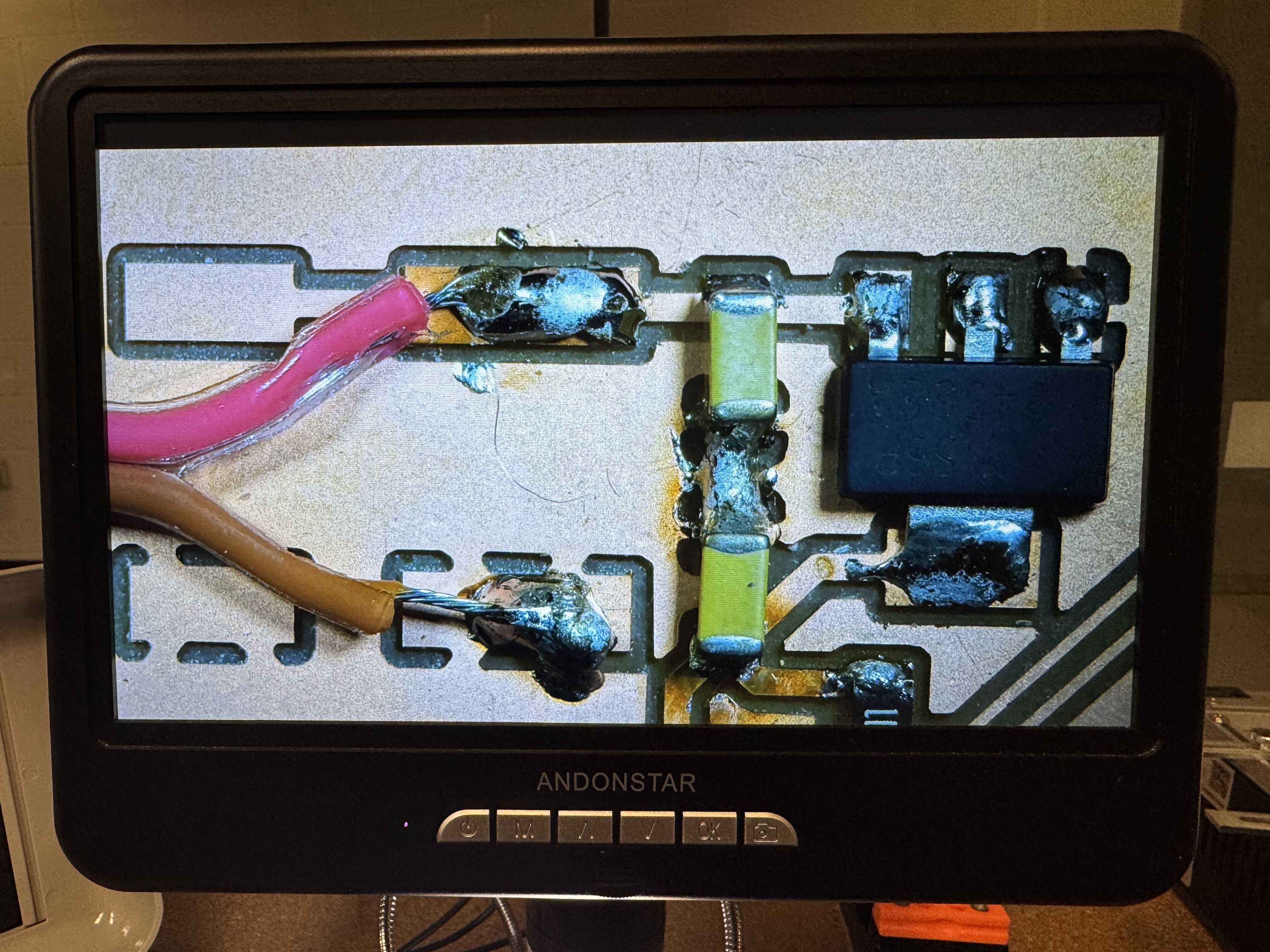
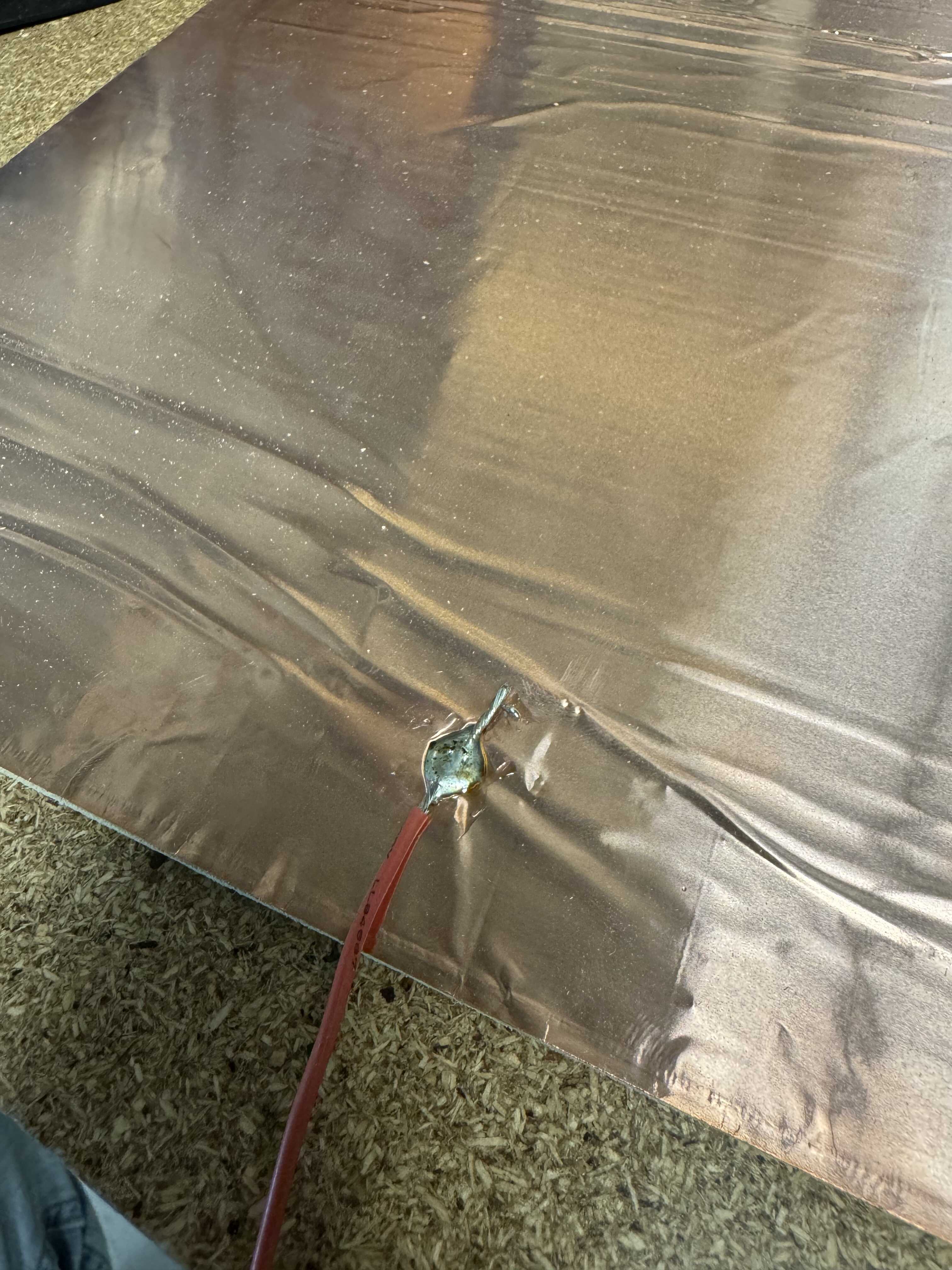
Alan had warned me that the laser can create shorts with the layer underneath. Though the board turned out beautifully, that was indeed an issue, so I didn’t end up using the aluminum board. The shorts were clear under the Lynx Evo, and I tried to take a picture below:
So, I went back to the Carvera flow. First, I figured out how to align the holes with the copper with Alan’s help. It turns out the that Edge Cuts file and the Front Copper file are slightly different sizes. The Edge Cuts file is 40.69mm x 40.69mm, while the Front Copper file is 39.639mm x 39.639mm (the actual board size is 40.64mm x 40.64mm). Mods seems to align the two files on the bottom-leftmost pixel, so the holes are .5255mm too high and .5255mm too far to the right. It turns out that gerber2img has an option to lock dimensions and coordinates, though. Thanks, Quentin! So, I processed the larger Edge Cuts file first, then locked dimensions and coordinates before processing the Front Copper file.
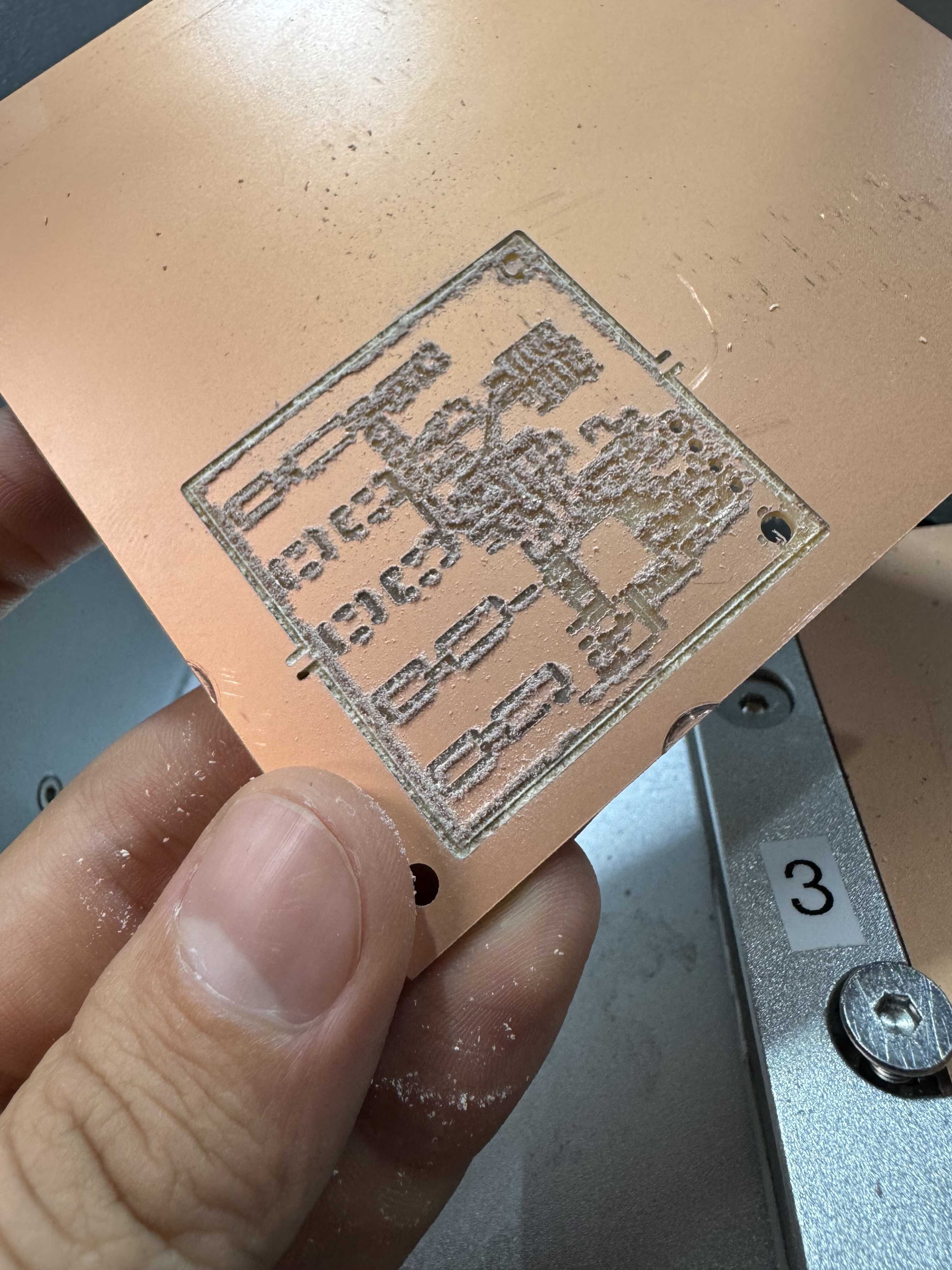
Then, I repeated the process from before. The alignment issue was gone, but the board came out very rough:
Based on my previous experience, I assumed this was due to a bad end mill. Visual inspection corroborated my suspicion, so I learned how to replace an end mill on the Carvera. After restarting the process, though, I noticed a similar result, and stopped the process.
As the process was stopping, I noticed that the Carvera was putting back the 1/32" end mill (tool #3) instead of the 1/64" end mill we had just replaced (tool #4). I realized that when I had tried to change the tool size from 0.4mm to 0.38mm as before, I accidentally changed the wrong field in mods. I had asked mods to use tool 3.8, which apparently rounded to tool 3. I fixed my issue and kicked off my fifth board.
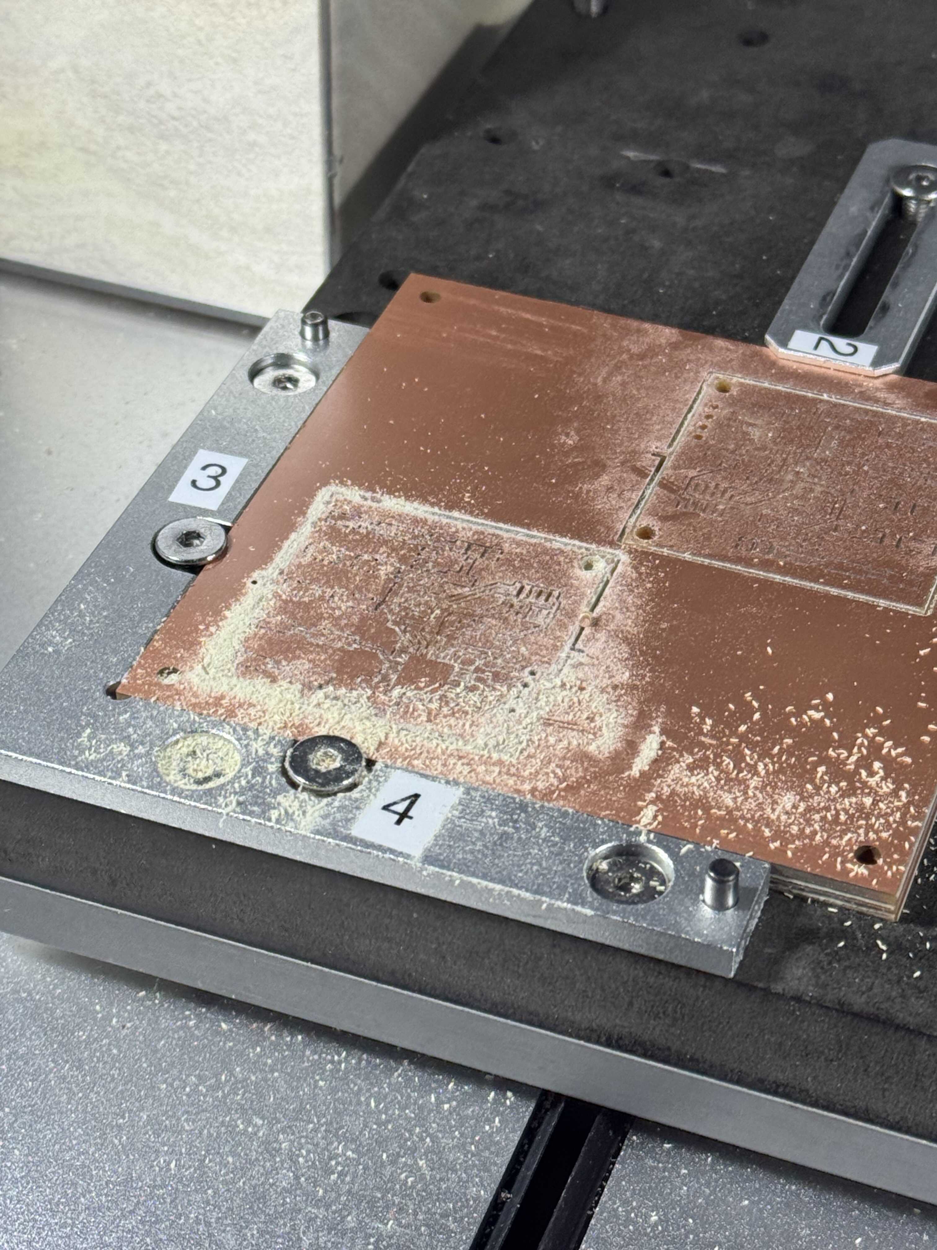
Unfortunately, I did not inspect the tool path carefully enough. The area we had used a the litmus test the first time (the bottom pad) was fine, but two shorts had snuck in on the TQFP footprint. It seemed that the .38mm setting did not do the trick this time. This is likely because I used a 1000 DPI image, and not a 2000 DPI image as before. I binary-searched and found that using this image, the largest tool size that produced no shorts was .35mm.
Finally, I was back to a functional board:
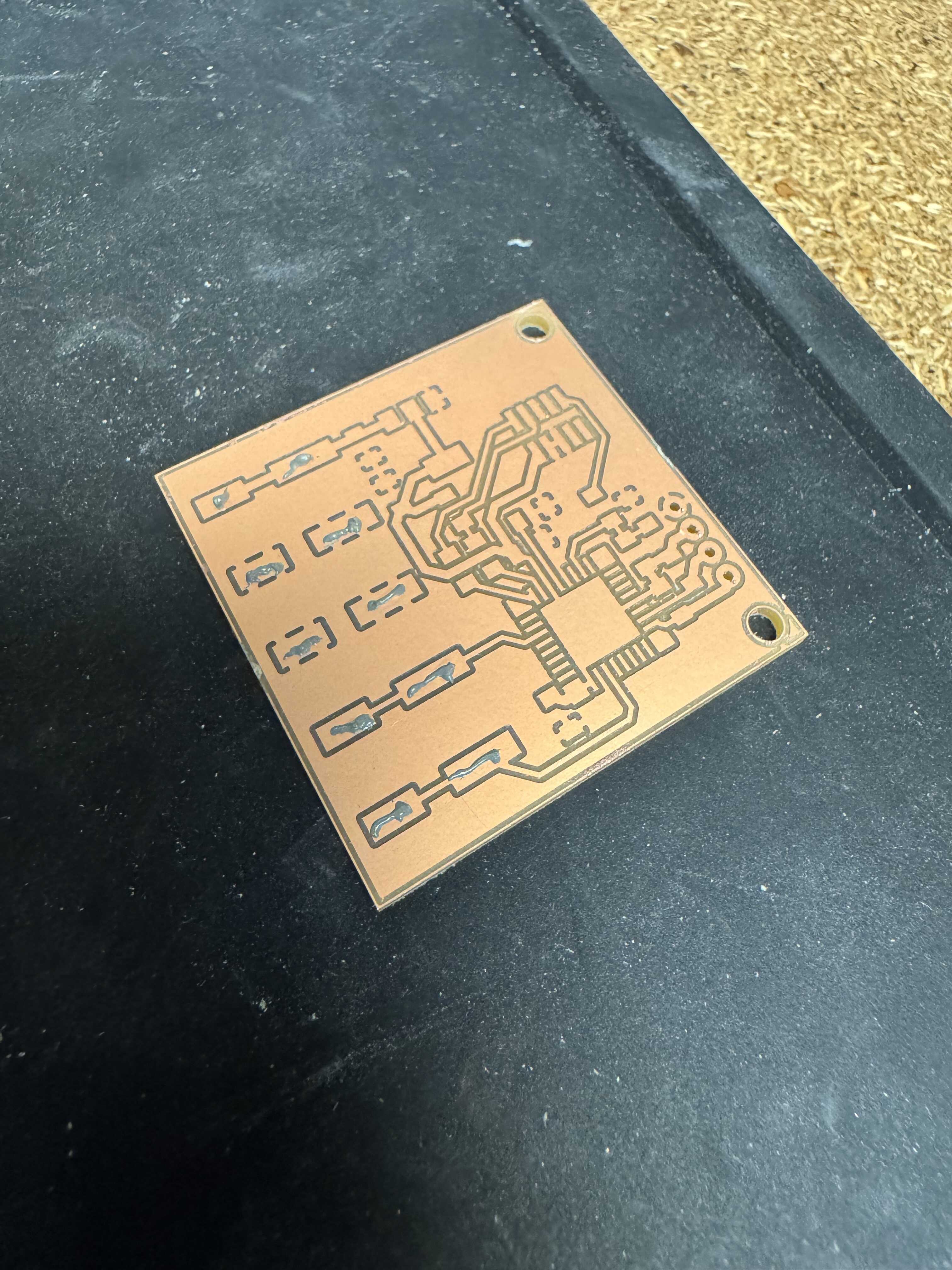
This time, I used paste for the microcontroller. I had the hot air turned up too much, but everything was connected correctly from the first try:
I placed the rest of the components using the wire solder:
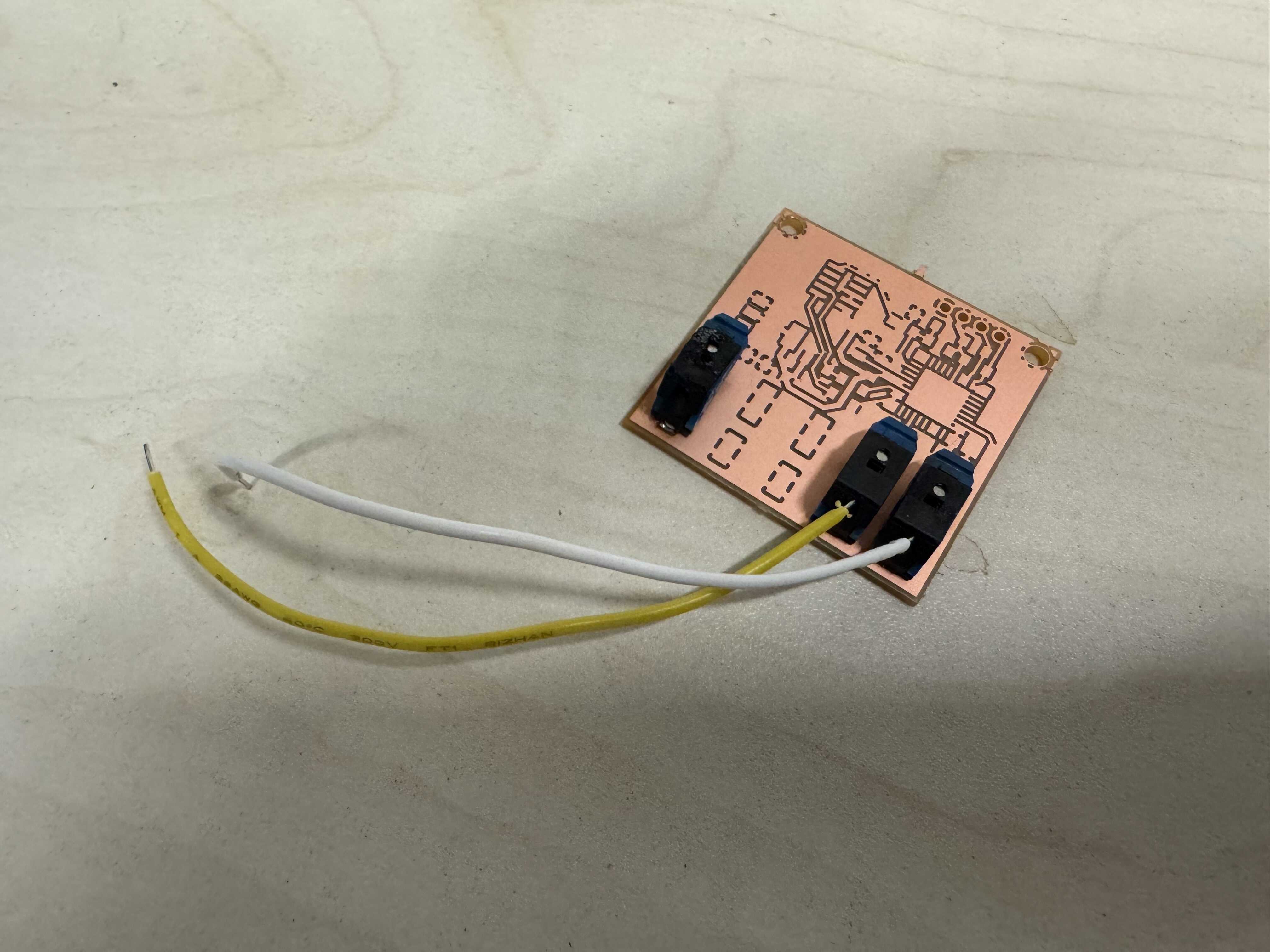
I did not attempt the connectors this time. Instead, I soldered wires directly. I tried using the ribbon cable instead of hook-up wire, as recommended:
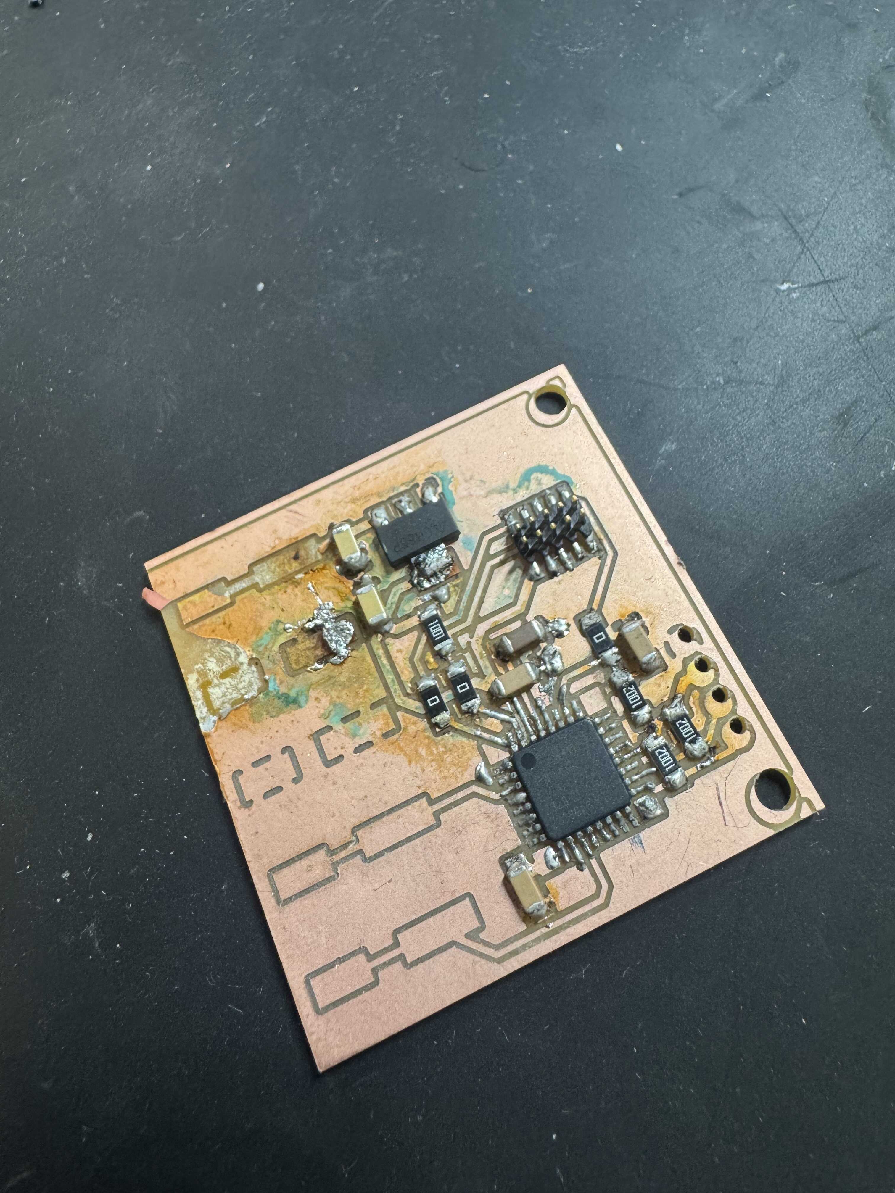
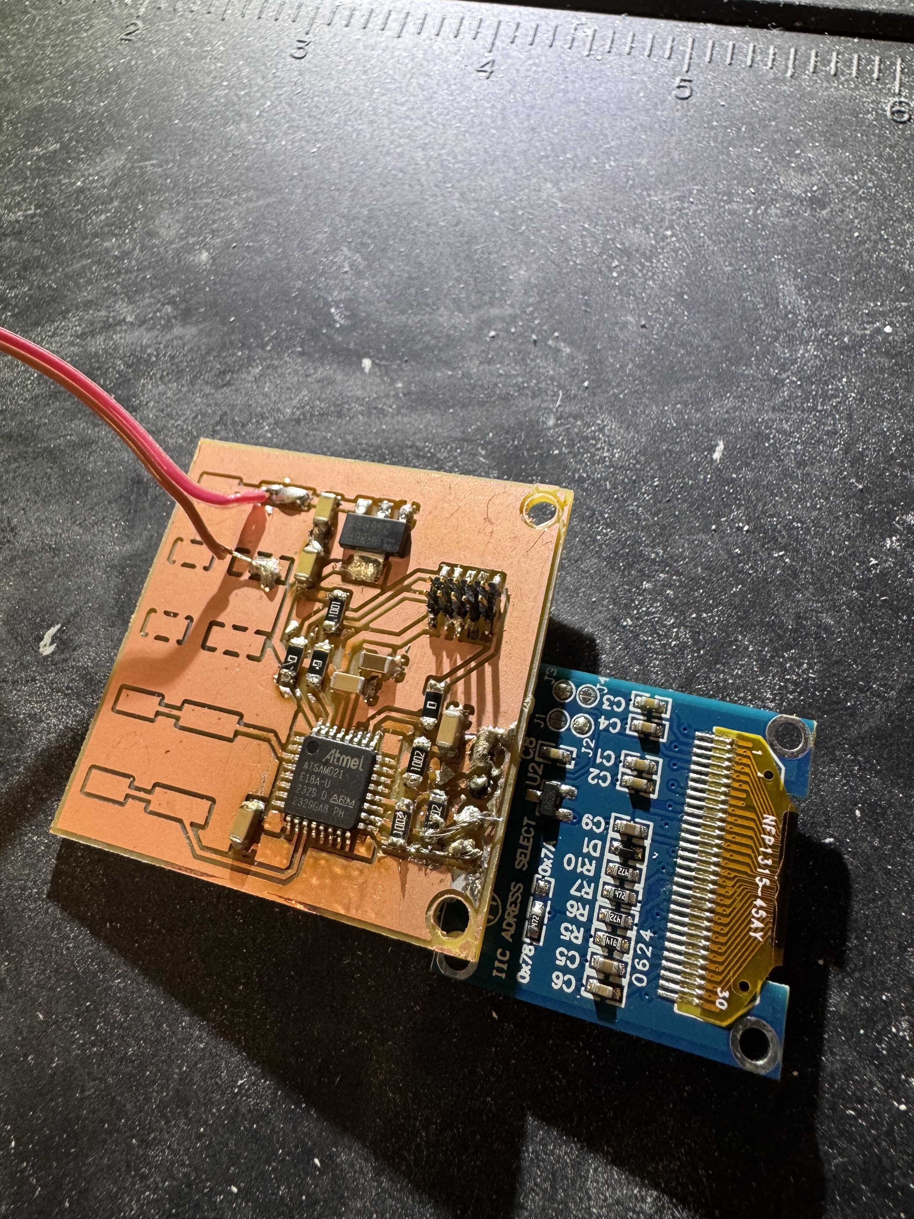
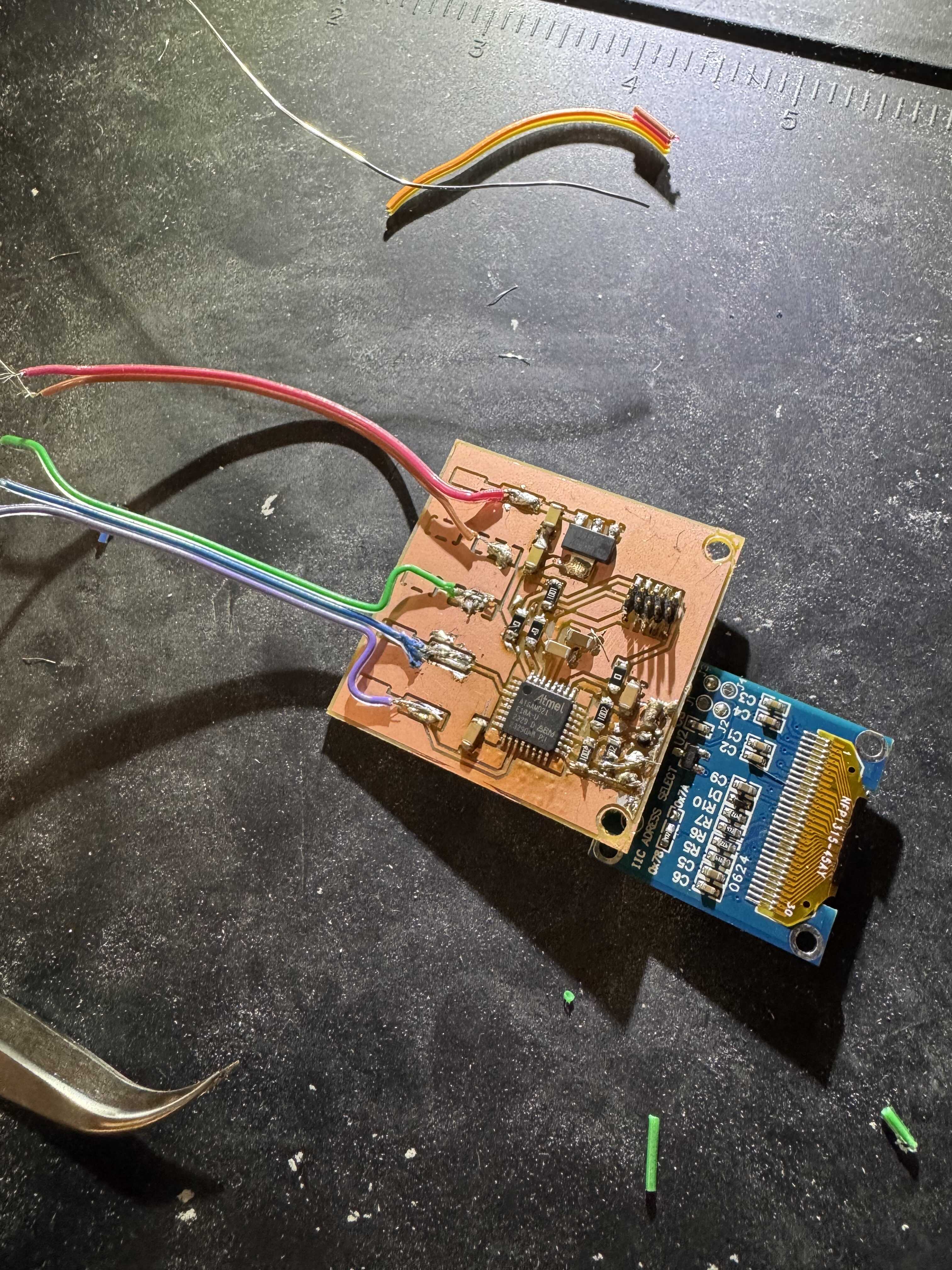
Surprisingly, the through-hole connections, which I waved off as the easiest thing, were a problem. I had used the 1.4mm holes, which are too large. The annular ring and the traces were too small, and I had my iron turned up way too high from soldering the ground wire right before hand. To avoid fabbing a seventh board, I did some surgery using strands from the ribbon cable.
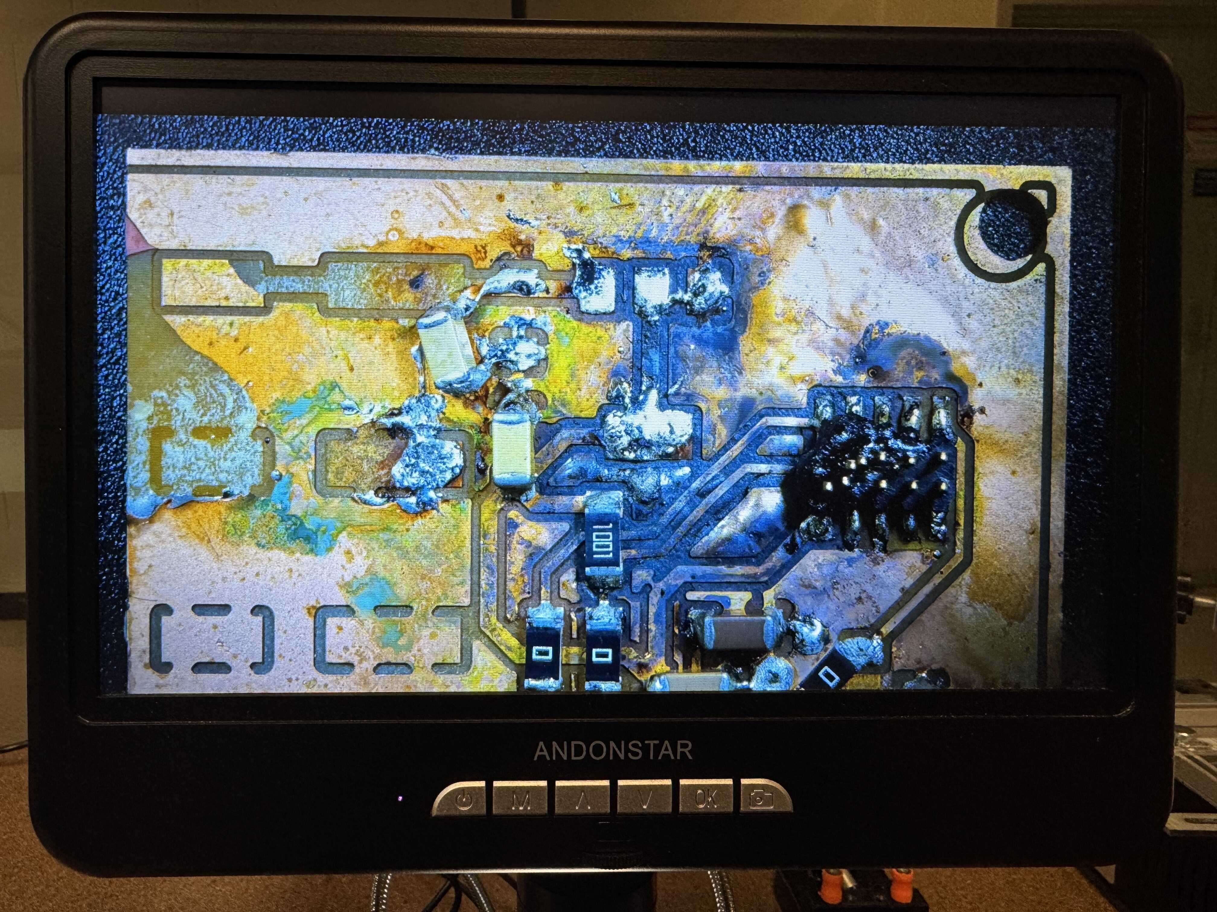
I was finally back to where I was before attempting to attach the terminals. This time, I took a picture:
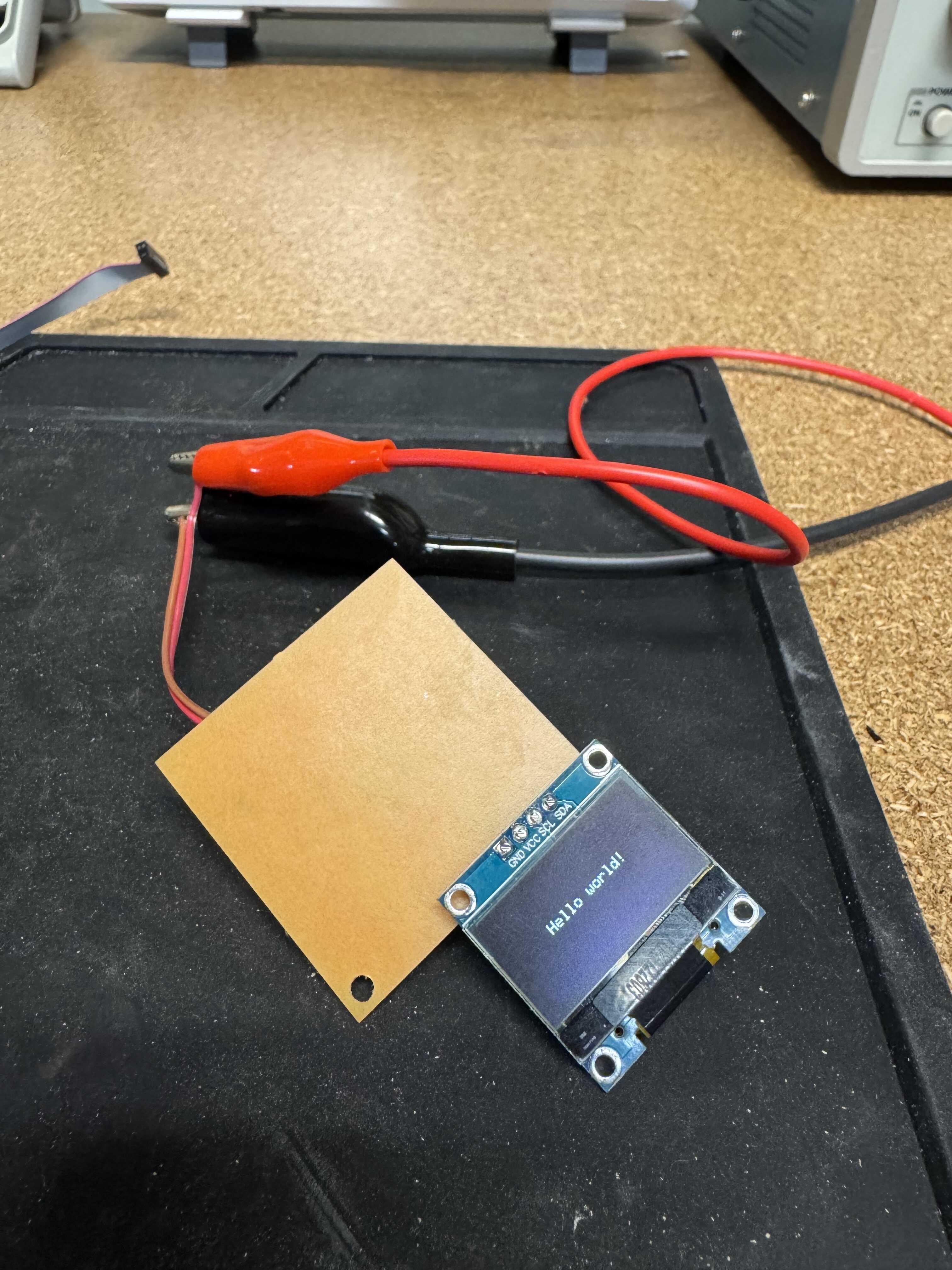
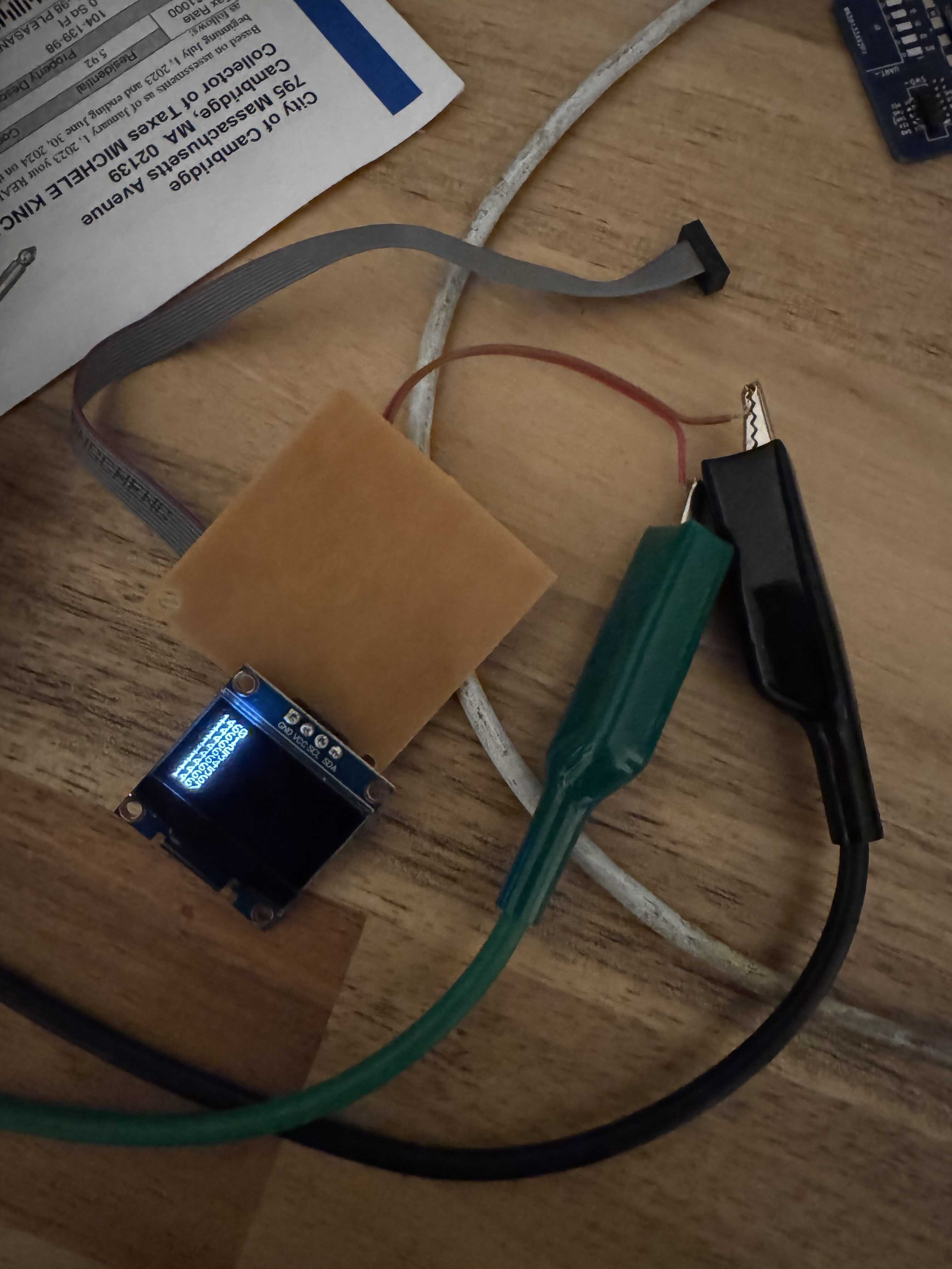
Despite a cold joint on the SDA connection, the board even survived a trip to my bench at home, where I piped the PTC output to the screen:
The next day, I added connections to the PTC inputs and moved on to the mechanical design.
Mechanical Design
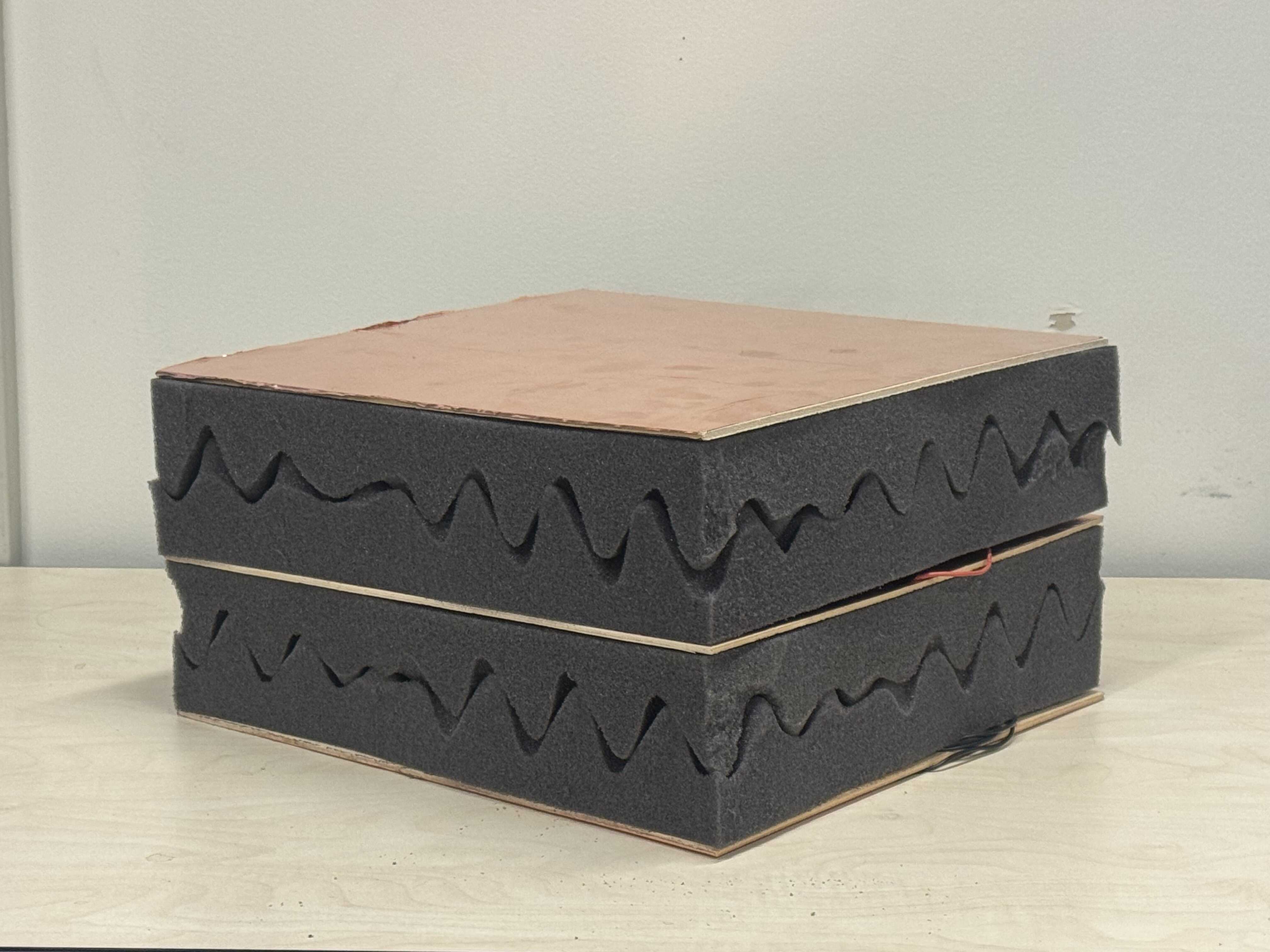
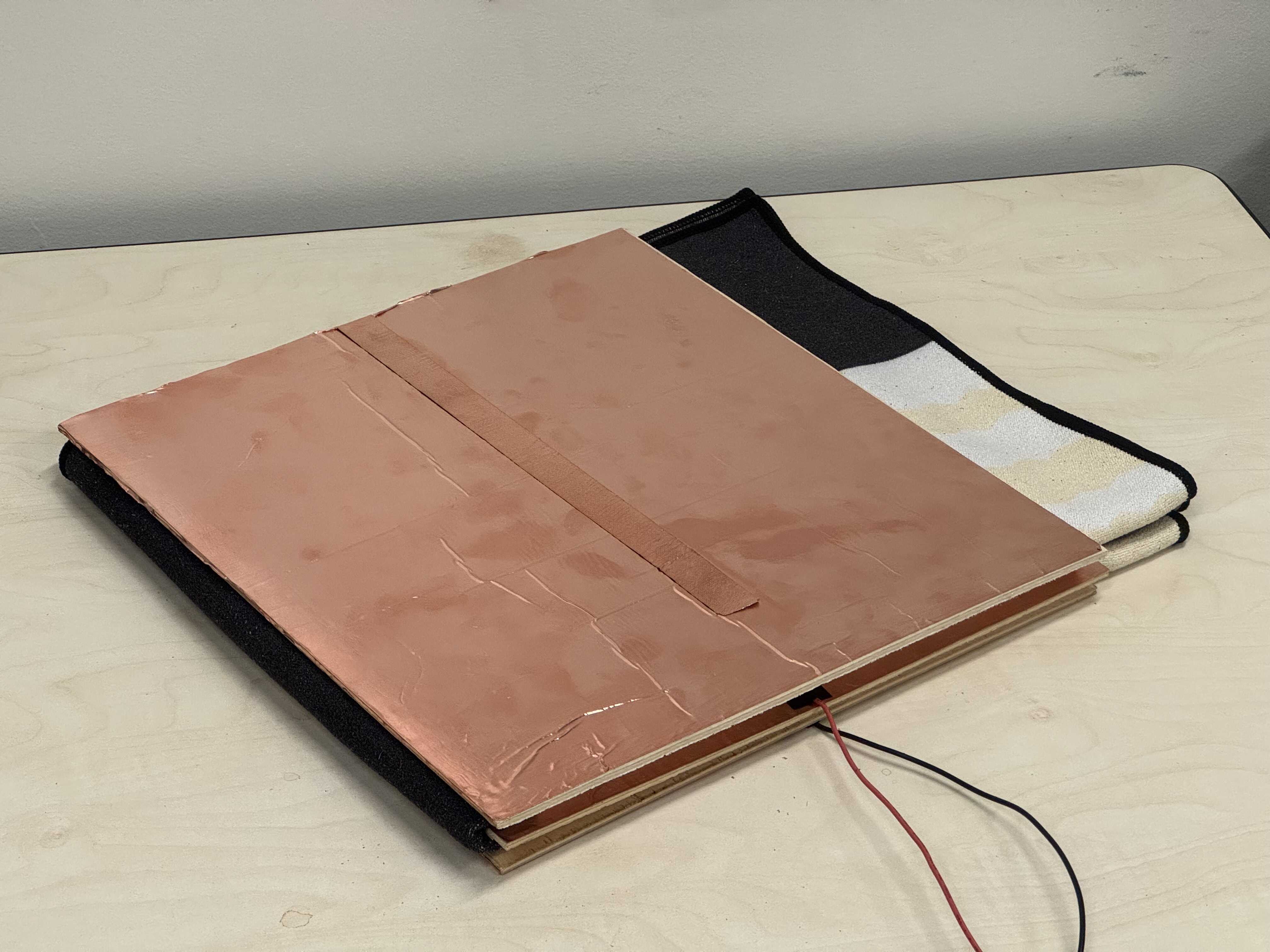
I used three plates for my scale. The bottom and the top, I connected to ground. The middle plate I connected to Y0. I made the plates out of wood, which I cut to shape on the bandsaw, and copper tape. I connected the two ground plates using copper tape as well. I soldered wires to the bottom and middle plates:
At first, I tried using packing foam between the plates. I cut matching pieces to size, again using the bandsaw:
Unfortunately, the material turned out to not be nearly compressible enough for any reasonable weight. So instead, I replaced it with a folded up towel, which ended up working really well:
I used free weights to calibrate the scale. In the region of operation, the relationship was close to linear. I hooked up the board to the plates, and hooked up 3 AA batteries to the board’s power input.
Unfortunately, I did not take a video. By the time I brought the device to demo in class, the cold joints on the OLED gave up, as was expected sooner or later.
Software
So, the software portion of the device is very straightforward.
I used the Adafruit_FreeTouch library for the PTC’s
and the Adafruit_SSD1306 for the OLED.
I didn’t get around to testing the mutual capacitance functionality of the PTC’s,
so the software is very similar to the program I wrote for Week 3.
It can be found here:
https://gitlab.cba.mit.edu/dimitar/kitchen-sink/-/tree/main/q_reader.
Board Fabrication, Round 2
After class, I wanted to rebuild the scale to at least get some pictures of it working. I had no interest in trying to salvage the broken board, opting instead to make a new one. This time, I fixed some things in the design. First of all, I changed my minimum clearance from 0.4mm to 0.44mm. I modified the design to pass DRC using the new rules. Also, I changed the through-hole size from 1.4mm to 1mm. I manually increased the copper around the holes up to the minimum clearance. When I went to fab, I almost made it without the mounting holes, which had disappeared when I updated from schematic to ingest the smaller through holes. Luckily, I caught that in time (and added the mounting holes to the schematic so it doesn’t happen again).
I also debugged the connectors a bit. Using one of my failed boards, I attempted paste and hot air again. I slowly raised the temperature until reflow succeeded at 170°C. The plastic was getting a little suspicious at that temperature, but it didn’t completely destroy the connectors. I ensured they made contact and there were no shorts.
I fabbed my seventh board, and started with the connectors:
For some reason, the process was not as smooth as it was for my test board. Out of 5 connectors, at 170°C, two worked, two fell off, and one caused a short to ground. I increased the temperature slightly to 174°C, which caused the plastic to melt a bit, but didn’t solve my problem.
Finally, I gave up on the SM99S01VBNN05G7.
I redesigned the board with a simple screw-terminal instead:
Then I re-fabbed it using the flow. The only hitch was that the default tab length in the mods program went underneath one of the through-holes, which I didn’t notice until after the milling was done. I found that the problem could be fixed by changing the length of the tab, but instead of re-milling, I just drilled out that hole manually.
Stuffing was mostly painless. I did short VDDCORE to a useless strip of ground pour on accident, which took me a while to find.
Other than that, I didn’t run into any issues.
I assembled the board back into the scale, and recalibrated.
It occurred to me that a “zero” button would have been a good idea.
I did have the X0 pin still pulled out in case I wanted to do mutual capacitance,
so I made that into a “button”.
A video of the assembled scale working is shown below:
Future Work
If I were to keep iterating, I would first pick a material that flexes less than the wood I picked. I would also try to find a better material for between the plates. Finally, I would explore the mutual capacitance functionality of the PTCs as I originally intended.
However, this is not a very good scale design (as expected). Particularly, the curve fit depends on the zero location, so a simple zeroing button isn’t enough to recalibrate it exactly correctly. And, it needs constant recalibration. However, while calibrated, it does function as a scale.
