Overview
This week dove into electronics design, moving from circuit concepts to a complete PCB design. The assignment required simulating a circuit and then using EDA (Electronic Design Automation) tools to design an embedded microcontroller system with components from our lab inventory. I designed a sensor board built around the XIAO-RP2040 microcontroller, featuring two inputs (phototransistor and thermistor) and two outputs (LED and speaker), creating a compact system that can respond to both light and temperature changes.
Circuit Simulation
Before committing to a physical PCB design, I started with circuit simulation to validate my design concept. Simulation is an essential step in electronics design - it allows you to test functionality, identify potential issues, and iterate quickly without the time and cost of fabricating physical boards.
Circuit simulation showing the interaction between sensors (phototransistor and thermistor) and outputs (LED and speaker)
The simulation demonstrated the core functionality of my design. The phototransistor acts as a light sensor, changing its conductivity based on ambient light levels. The thermistor provides temperature sensing by varying its resistance with temperature changes. These two input signals are processed by the microcontroller, which then controls the LED for visual feedback and the speaker for audio output. Being able to see the circuit behavior in simulation gave me confidence that the design logic was sound before moving to schematic capture.
Schematic Design

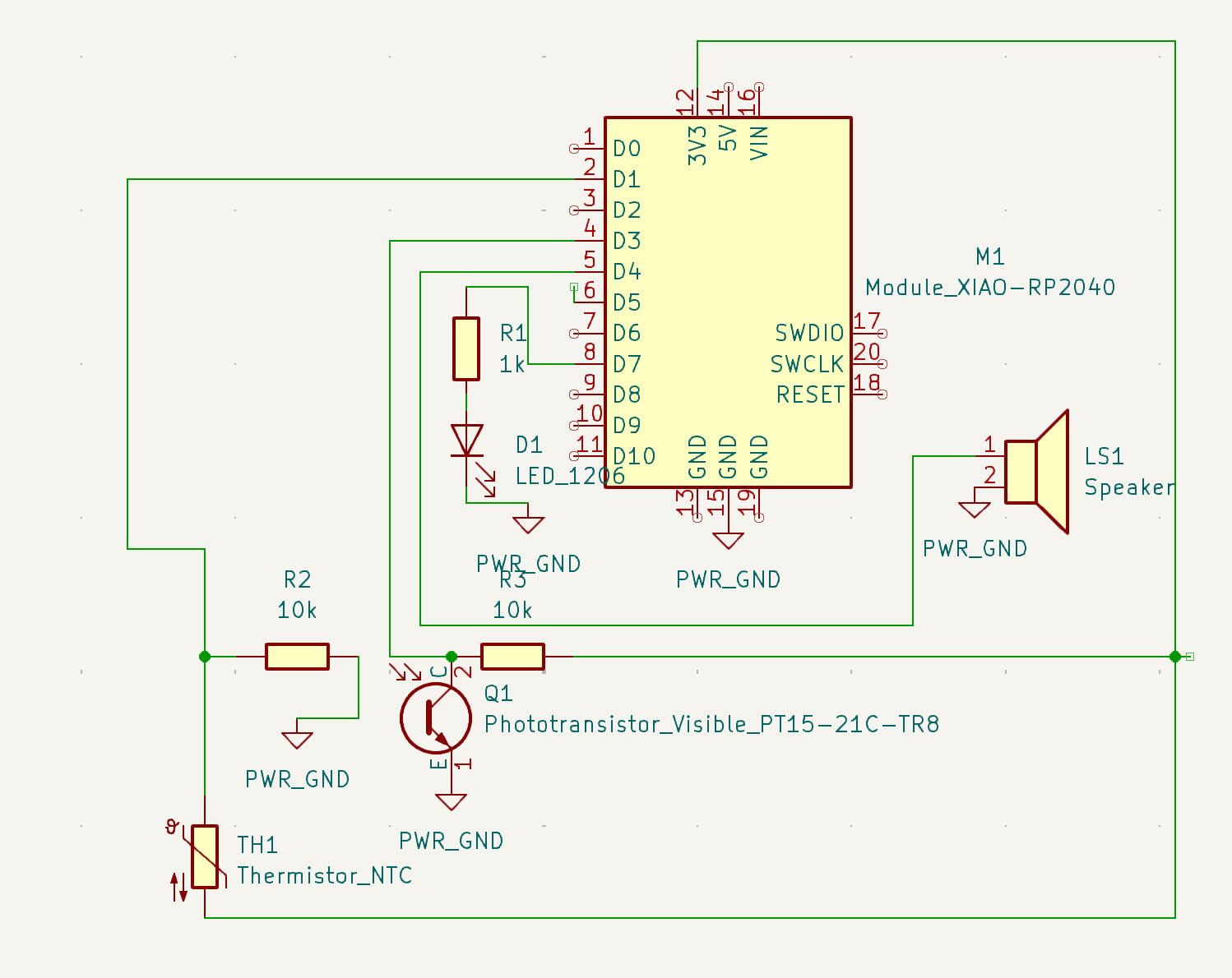
Complete schematic showing microcontroller connections to sensors and actuators
With the simulation validated, I moved to creating the formal schematic in KiCad. The schematic serves as the logical representation of the circuit, showing how components connect electrically without worrying about physical placement yet. This is where component selection becomes critical - I needed to choose parts that were not only functionally appropriate but also available in our lab inventory and suitable for the fabrication process.
Component Selection
At the heart of the design is the Seeed Studio XIAO-RP2040 microcontroller. This compact board features the Raspberry Pi RP2040 chip with dual ARM Cortex-M0+ cores running at 133 MHz, 264KB of SRAM, and 2MB of flash memory. The XIAO form factor is incredibly small (20mm x 17.5mm), making it perfect for compact embedded projects while still providing 11 GPIO pins with various capabilities including ADC, I2C, SPI, and UART. The built-in USB-C connector simplifies programming and power delivery, and the RP2040's robust peripheral set makes it ideal for handling multiple sensors and outputs simultaneously.
For the light sensor, I selected the Phototransistor_Visible_PT15-21C-TR8, a visible light phototransistor that provides good sensitivity across the visible spectrum. This component acts like a transistor where the base current is controlled by incident light rather than an electrical signal. As light intensity increases, the phototransistor allows more current to flow, creating a voltage signal that the XIAO-RP2040's ADC (Analog-to-Digital Converter) can read.
The temperature sensing uses a Thermistor_NTC (Negative Temperature Coefficient), which decreases its resistance as temperature increases. By placing it in a voltage divider circuit with a fixed resistor, the changing resistance produces a varying voltage that correlates with temperature. The XIAO-RP2040 reads this voltage through another ADC channel and can calculate the actual temperature or simply use it as a relative temperature indicator.
For outputs, I included an LED with an appropriate current-limiting resistor to provide visual feedback, and a speaker for audio alerts. The speaker connects through a transistor driver circuit since the XIAO-RP2040's GPIO pins can't directly provide enough current to drive a speaker effectively. The RP2040's PWM capabilities allow for generating tones at various frequencies for the speaker.
Design Considerations
The schematic incorporates several important design principles. Pull-up or pull-down resistors ensure that inputs have defined states, decoupling capacitors near the microcontroller stabilize the power supply, and proper current limiting protects components from damage. Each connection is labeled clearly, making it easier to troubleshoot and understand the circuit later. The schematic also includes standard features like a programming header for uploading code to the microcontroller and test points for debugging.
PCB Layout Design

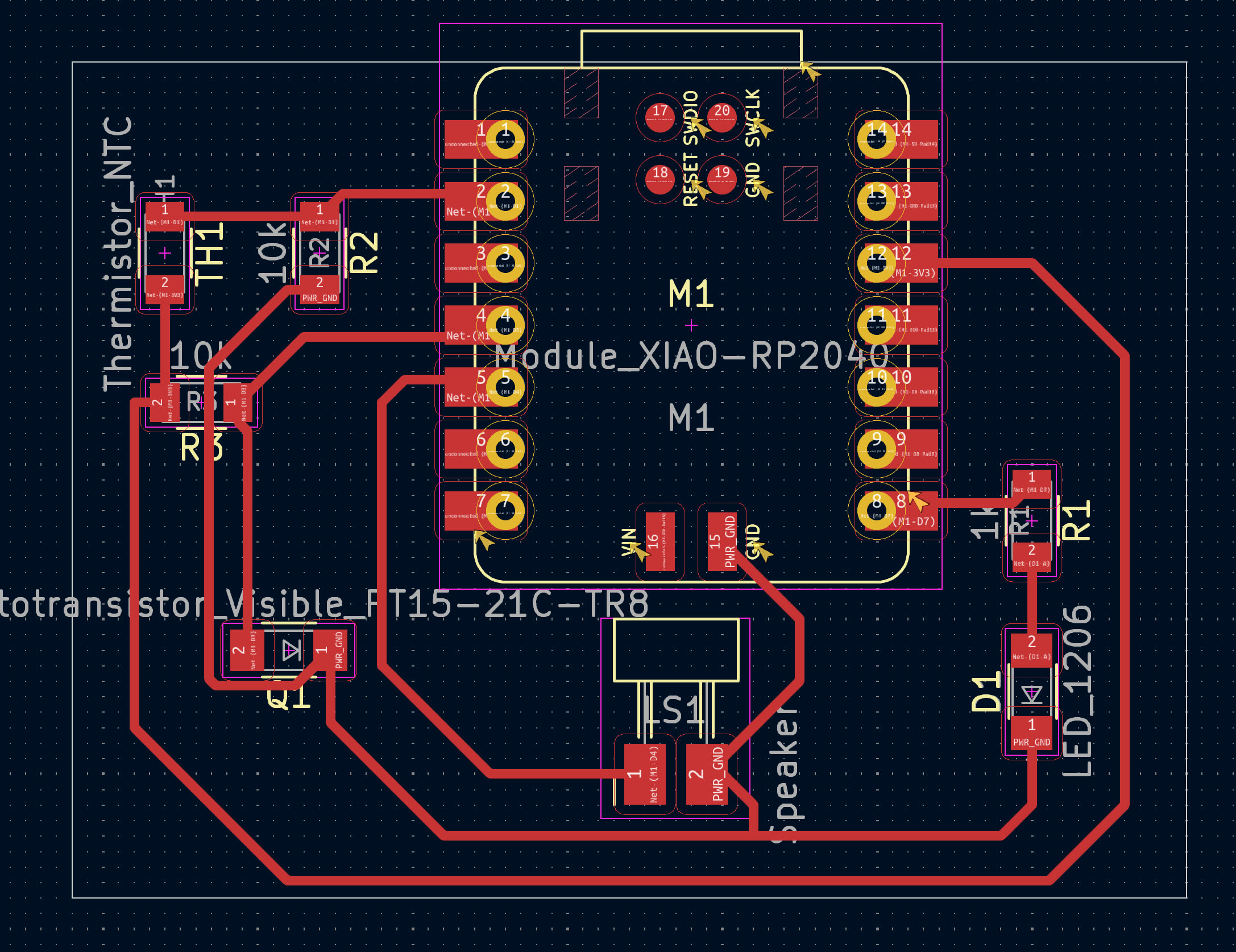
PCB layout showing component placement and copper trace routing
Translating the schematic into a physical PCB layout is where electronic design becomes an art as much as a science. The layout process involves placing components on the board and routing copper traces to create the electrical connections shown in the schematic. However, unlike the schematic, the PCB layout must consider physical constraints, manufacturing limitations, and electrical performance issues like signal interference and heat dissipation.
I started by placing the major components strategically. The microcontroller goes in a central location since it connects to many other parts. The sensors (phototransistor and thermistor) needed to be positioned where they could effectively sense their respective environmental parameters - the phototransistor near the board edge where it can receive ambient light, and the thermistor positioned away from heat-generating components to get accurate temperature readings.
Routing the traces requires careful thought about trace width (which affects current capacity), spacing (which affects manufacturing reliability), and path (which affects signal quality). I kept power traces wider to handle higher current, maintained adequate spacing between traces to prevent short circuits during fabrication, and tried to minimize trace lengths to reduce resistance and potential noise. The board includes a ground pour - a large area of copper connected to ground - which improves signal integrity and makes fabrication more reliable.

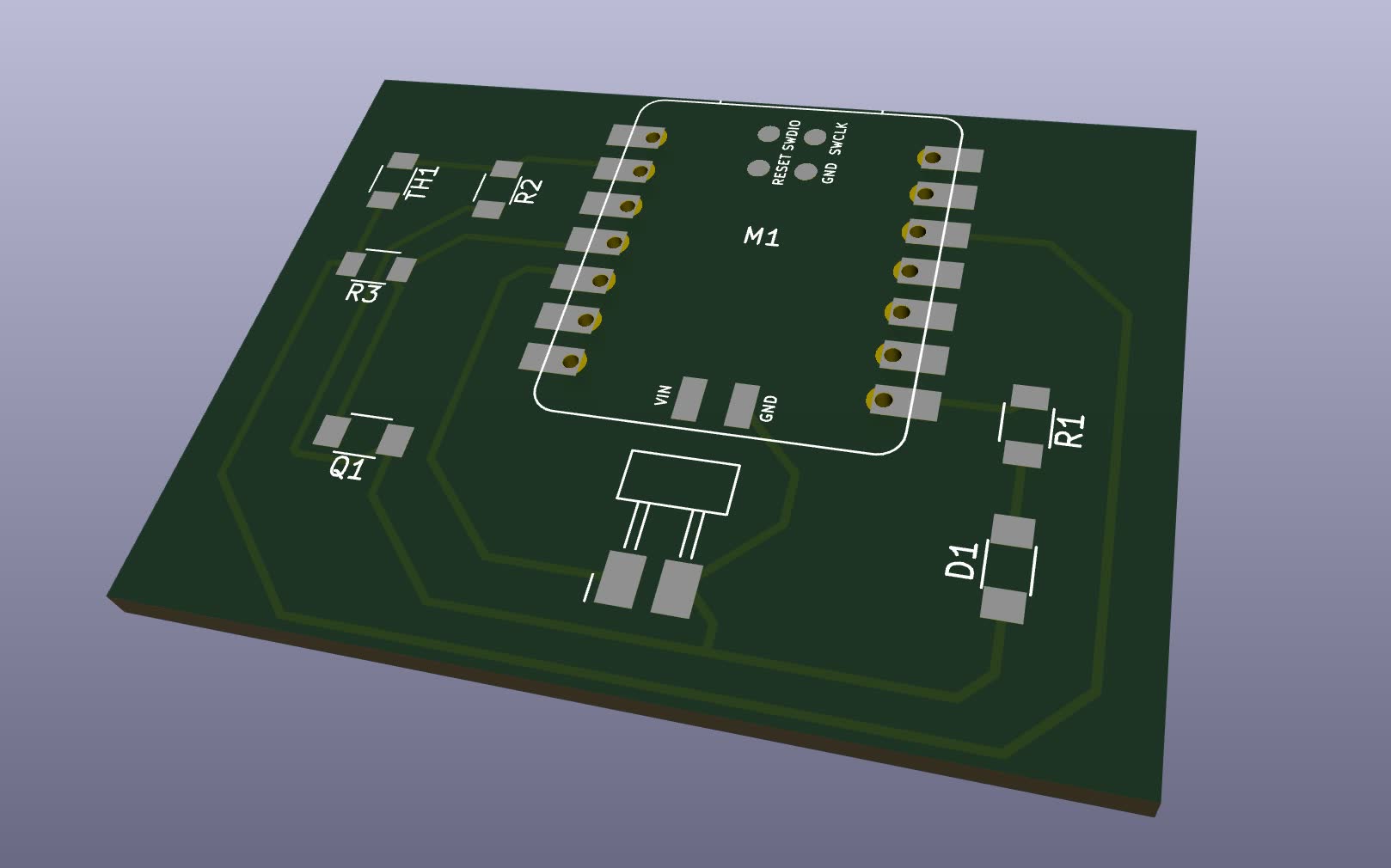
3D visualization of the PCB showing component placement and board structure
The 3D view in KiCad helps visualize the final board, showing component heights and potential mechanical interferences. This view revealed that the speaker would be the tallest component, which is fine for this design but might be a consideration if the board needed to fit in a specific enclosure.
Design Rule Check (DRC)

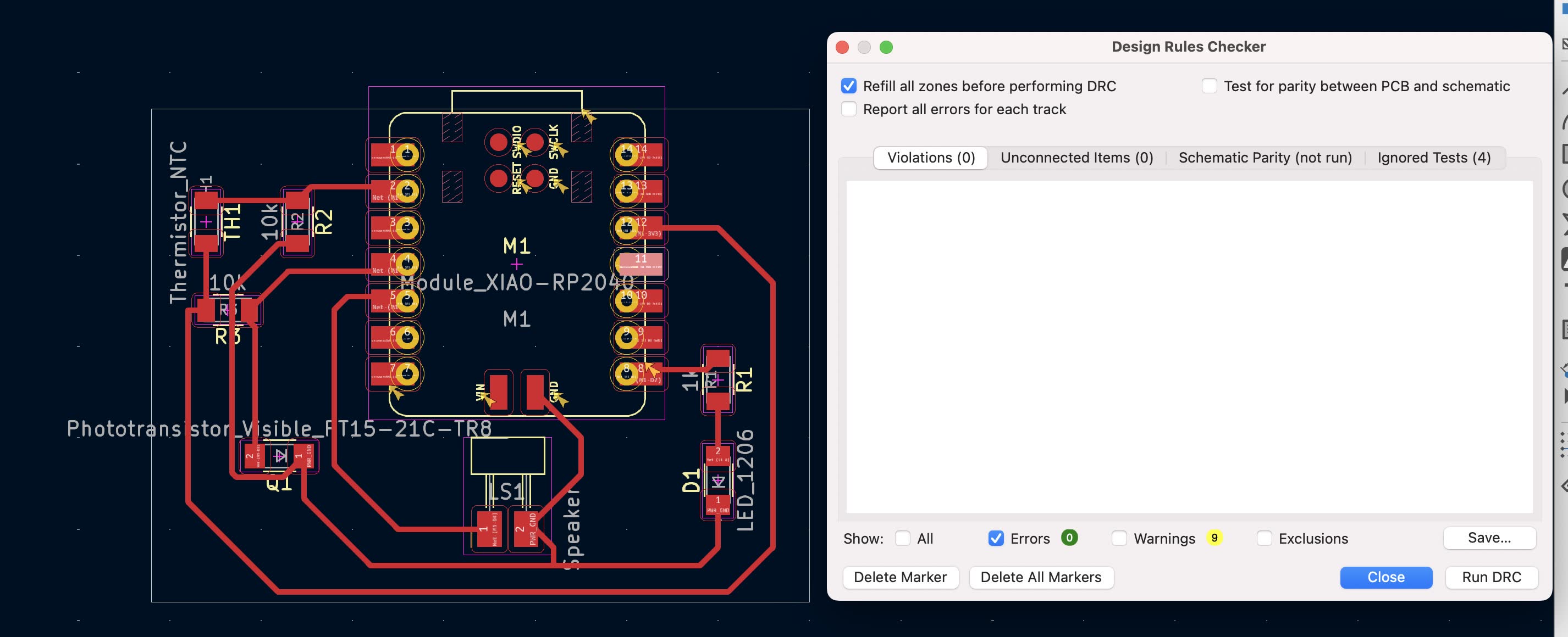
Design rule checker confirming the PCB meets all fabrication requirements
Before sending a design to fabrication, it's essential to run a Design Rule Check (DRC). The DRC verifies that the PCB layout complies with the manufacturing capabilities of the fabrication process. Different fabrication methods have different limitations - for example, our lab's PCB milling machine can't create traces narrower than a certain width or space them closer than a certain distance.
I configured the DRC with our lab's manufacturing constraints: minimum trace width, minimum trace spacing, minimum drill hole size, and clearances around pads. Running the check identified a few issues in my initial layout where traces were too close together or where component pads overlapped with ground pour in problematic ways. After adjusting these issues and re-running the DRC until it showed no errors, I could be confident that the design is manufacturable.
The DRC also performs an Electrical Rule Check (ERC) that looks for logical problems like unconnected pins that should be connected, or power nets that aren't properly connected to power sources. These checks catch mistakes that might not be obvious from visual inspection but would cause the circuit to malfunction.
Technical Specifications
Input Circuits
Phototransistor (PT15-21C-TR8): Connected in a common-emitter configuration with the collector connected through a pull-up resistor to VCC. The voltage at the collector varies inversely with light intensity. The microcontroller's ADC reads this voltage to determine light levels. The visible light spectrum sensitivity makes this ideal for ambient light detection in typical indoor and outdoor environments.
Thermistor (NTC): Configured in a voltage divider with a fixed 10kΩ resistor. At 25°C, the thermistor has a nominal resistance of 10kΩ, creating a half-supply voltage at the divider midpoint. As temperature rises, the NTC resistance drops, changing the divider voltage. The microcontroller reads this voltage and can convert it to temperature using the Steinhart-Hart equation or a lookup table.
Output Circuits
LED Indicator: A standard LED with a 330Ω current-limiting resistor, providing approximately 10mA of current for visible brightness without exceeding the microcontroller GPIO current limit. The LED can be used to indicate sensor states, errors, or general status information.
Speaker: Driven through an NPN transistor (likely 2N3904 or similar) in a switching configuration. The microcontroller GPIO controls the transistor base through a 1kΩ resistor, allowing the transistor to switch speaker current on and off. By toggling the GPIO at audio frequencies, the microcontroller can generate tones for alerts or simple audio feedback.
PCB Specifications
| Parameter | Value | Notes |
|---|---|---|
| Board Dimensions | ~50mm x 40mm | Compact size for prototyping |
| Layer Count | 2 layers | Top copper + bottom copper |
| Minimum Trace Width | 0.4mm | Based on milling machine capability |
| Minimum Trace Spacing | 0.4mm | Prevents shorts during fabrication |
| Via Diameter | 0.8mm | Standard size for through-hole vias |
Design Workflow and Tools
This project utilized KiCad as the primary EDA tool. KiCad is an open-source electronics design suite that's become increasingly popular due to its powerful features, active development, and zero licensing costs. The workflow progressed through several distinct stages:
Schematic Capture: Using KiCad's Eeschema, I created the circuit schematic by placing component symbols and drawing connections. The symbol library includes thousands of standard components, though I had to create custom symbols for some specific parts in our inventory. Each component gets a unique reference designator (R1, C1, U1, etc.) and a footprint assignment that links the logical symbol to its physical package.
Footprint Assignment: The critical step of linking each schematic symbol to a physical footprint determines how components will appear on the PCB. A resistor might be available in different packages (through-hole, surface-mount, various sizes), so selecting the right footprint for what's available in inventory is essential.
PCB Layout: KiCad's Pcbnew tool imports the schematic with all connections shown as "ratsnest" lines - straight lines indicating required connections. The layout process involves placing components and routing copper traces to replace the ratsnest lines with actual copper paths. The interactive router makes this process relatively smooth, suggesting trace paths and avoiding design rule violations.
Verification: Multiple verification steps ensure correctness - the DRC checks manufacturing feasibility, the ERC validates electrical logic, and the 3D viewer helps identify mechanical issues. These tools catch most problems before fabrication, saving time and materials.
Key Learnings
From Simulation to Reality
Working through the complete design flow from simulation to manufacturable PCB revealed the complexity hidden in electronic devices. Simulation helps validate concepts, but real PCB design requires considering many additional factors - component availability, physical size constraints, manufacturing tolerances, thermal management, and mechanical robustness. The iterative nature of the process, constantly moving between schematic, layout, and verification, helps refine the design incrementally.
Design Rules and Manufacturing Constraints
Understanding manufacturing limitations early in the design process is crucial. Our lab's PCB milling machine has different capabilities than commercial PCB fabrication services, which affects trace widths, spacing, and hole sizes. Designing with these constraints in mind from the start prevents having to redesign later. The DRC tools codify these constraints, making them explicit and automatically checkable rather than relying on manual verification.
Component Selection and Circuits
Choosing the right components involves balancing many factors. The PT15-21C-TR8 phototransistor provides good sensitivity but requires careful biasing to get useful voltage ranges for the ADC. The NTC thermistor offers excellent temperature sensitivity but needs calibration for accurate absolute temperature readings. Understanding these component characteristics and how to design appropriate interface circuits is fundamental to successful electronics design.
The Value of EDA Tools
Modern EDA software dramatically accelerates electronics development. KiCad's schematic capture prevents wiring mistakes, its footprint library handles component geometry, the interactive router speeds up layout, and automated checking catches errors. Without these tools, designing even a simple board would take much longer and be far more error-prone. Learning to use EDA tools effectively is as important as understanding circuit theory.
Next Steps
With the design complete and verified, the next phase will be fabricating the PCB. This involves milling the copper-clad board on our lab's CNC machine, drilling holes for through-hole components and vias, and then soldering all the components. Once assembled, I'll program the microcontroller to read the sensors and control the outputs, creating a functional environmental monitoring and feedback system. The real test will be seeing if the physical board performs as the simulation predicted!