Overview
This week brought my PCB design from Week 5 into physical reality through the electronics production process. The assignment required fabricating and testing the embedded microcontroller system I had designed, using our lab's PCB milling machine. This involved generating toolpaths, configuring the CNC mill, cutting the board, and learning important lessons about design margins and manufacturing constraints along the way.
Toolpath Generation
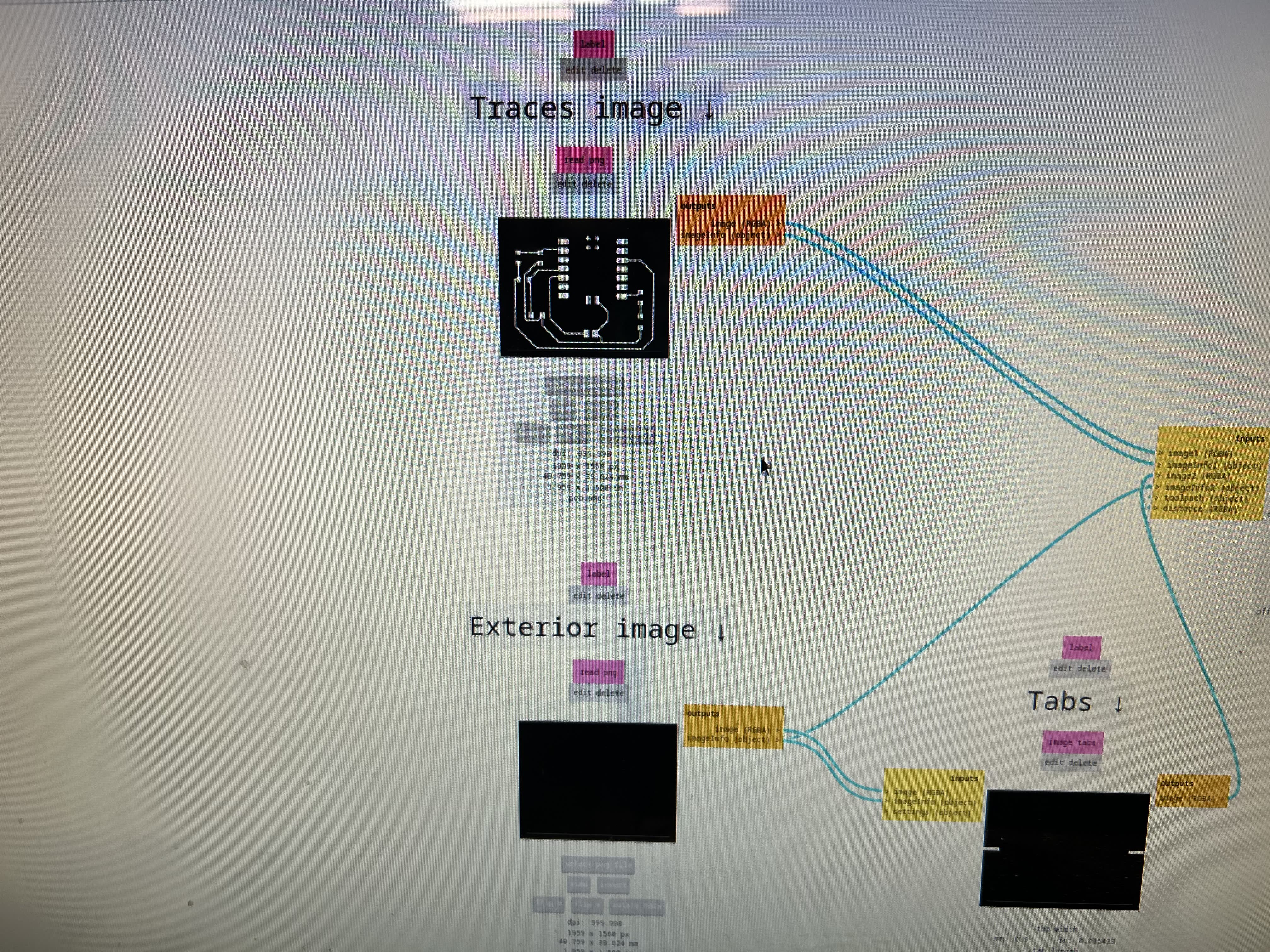
Using the toolpath generator to convert PCB design into machine instructions
The first step in PCB fabrication is converting the electronic design files into toolpaths that the CNC milling machine can follow. I used mods (modular CAM workflows) to process my PCB design files and generate G-code - the language CNC machines understand. The toolpath generator requires several key inputs: the trace image (showing where copper should remain), the outline cut path, drill locations, and critically, the tool specifications.
Understanding End Mill Selection
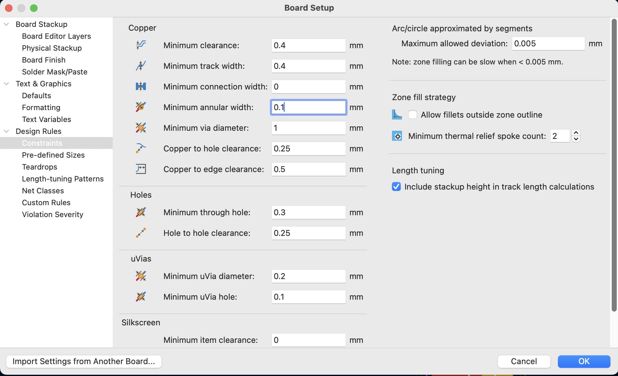
Measuring the end mill diameter - critical for accurate toolpath generation
Choosing and properly specifying the end mill is crucial for successful PCB milling. I used a 1/64" (approximately 0.4mm) end mill for tracing the copper traces - this small diameter allows for fine detail and tight spacing between traces. The tool diameter must be accurately entered into the toolpath generator because it determines how the machine offsets its path to achieve the desired copper removal. Even a small error in tool diameter specification can result in traces that are too wide or too narrow, potentially causing shorts or breaks in the circuit.
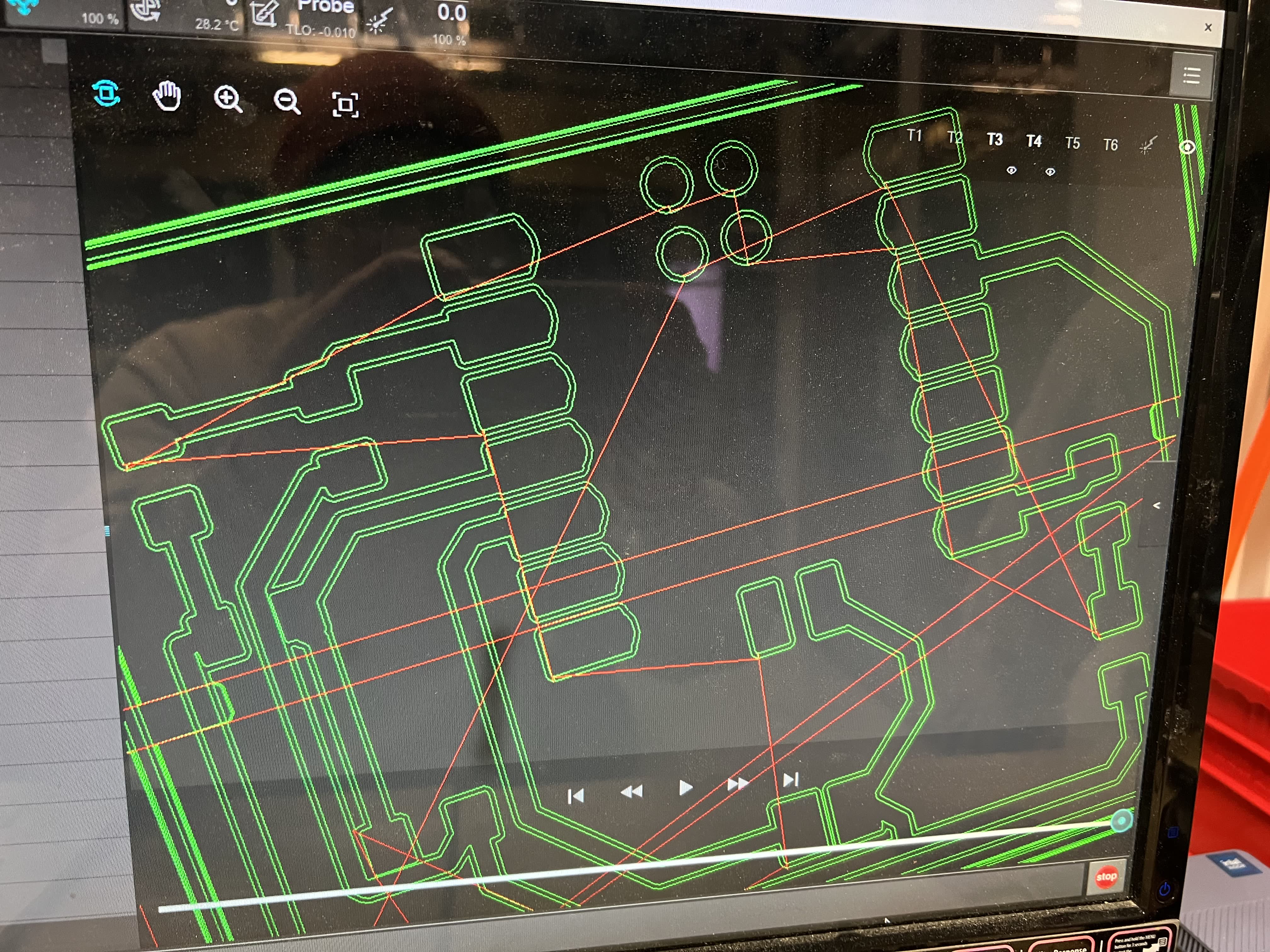
Visualizing the generated toolpath before sending to the machine
The toolpath visualization is an essential verification step. It shows exactly where the tool will move and how much material it will remove. I could see the trace paths (where copper between traces gets milled away), the outline cut (where the board edges are defined), and any drill holes. This preview revealed an issue with my initial design that would have caused problems during fabrication.
Design Iteration: Learning from the First Attempt
First design attempt showing the edge cut problem - tabs intruded into the PCB area
When I generated the initial toolpaths, I discovered a significant design flaw: my edge cut outline was too small. PCB milling typically uses "tabs" - small bridges of material that hold the board in place during cutting and prevent it from shifting. However, because my edge cut boundary was placed too close to my actual circuit, the tabs ended up intruding into the PCB design area itself. This would have resulted in tabs overlapping with copper traces or component pads, making the board unusable.
This taught me an important lesson about design margins. When designing PCBs for milling, you need to leave adequate space between your circuit elements and the board edge - not just for mechanical reasons, but to accommodate the fabrication process itself. The tabs need somewhere to attach that won't interfere with the electronics. I went back to my PCB design in KiCad and expanded the board outline, creating a larger clearance zone around my circuit.
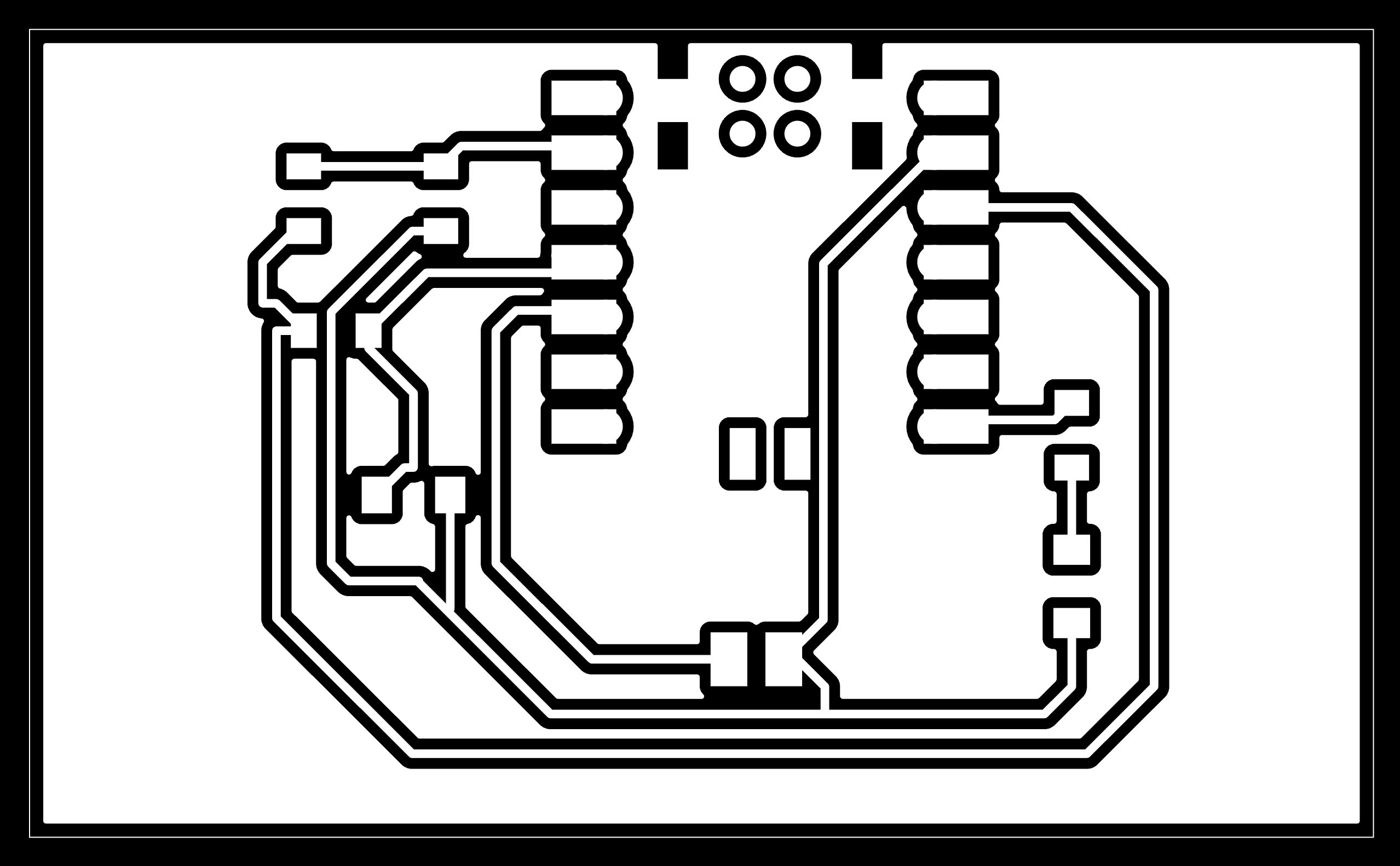
Revised PCB design with larger edge cut boundary providing proper clearance for tabs
The revised design incorporated a larger margin between the circuit and the board edge. This seemingly simple change made all the difference - the tabs could now be positioned in the empty border area without interfering with any circuit elements. It's these kinds of practical manufacturing considerations that don't show up in circuit simulations but are crucial for successful physical production.
Machine Setup and Configuration
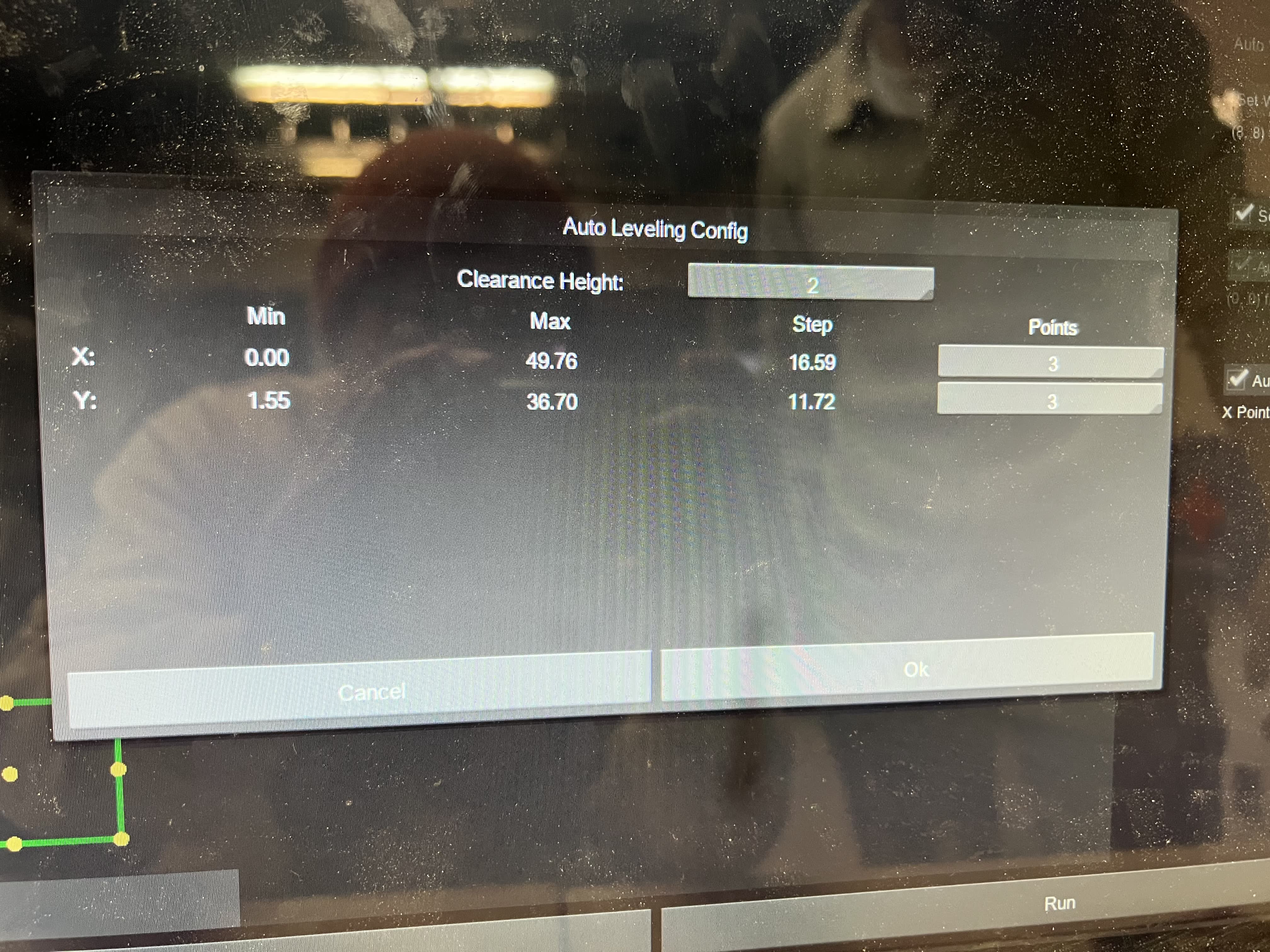
Configuring the CNC mill parameters for PCB production
Setting up the CNC milling machine properly is essential for good results. The process involves several critical steps: mounting the copper-clad board securely to the machine bed, installing the correct end mill in the spindle, and most importantly, zeroing the machine. Zeroing establishes the coordinate system that relates the toolpaths to the physical board position. Luckily, the machine can do all this process automatically.
Milling Process
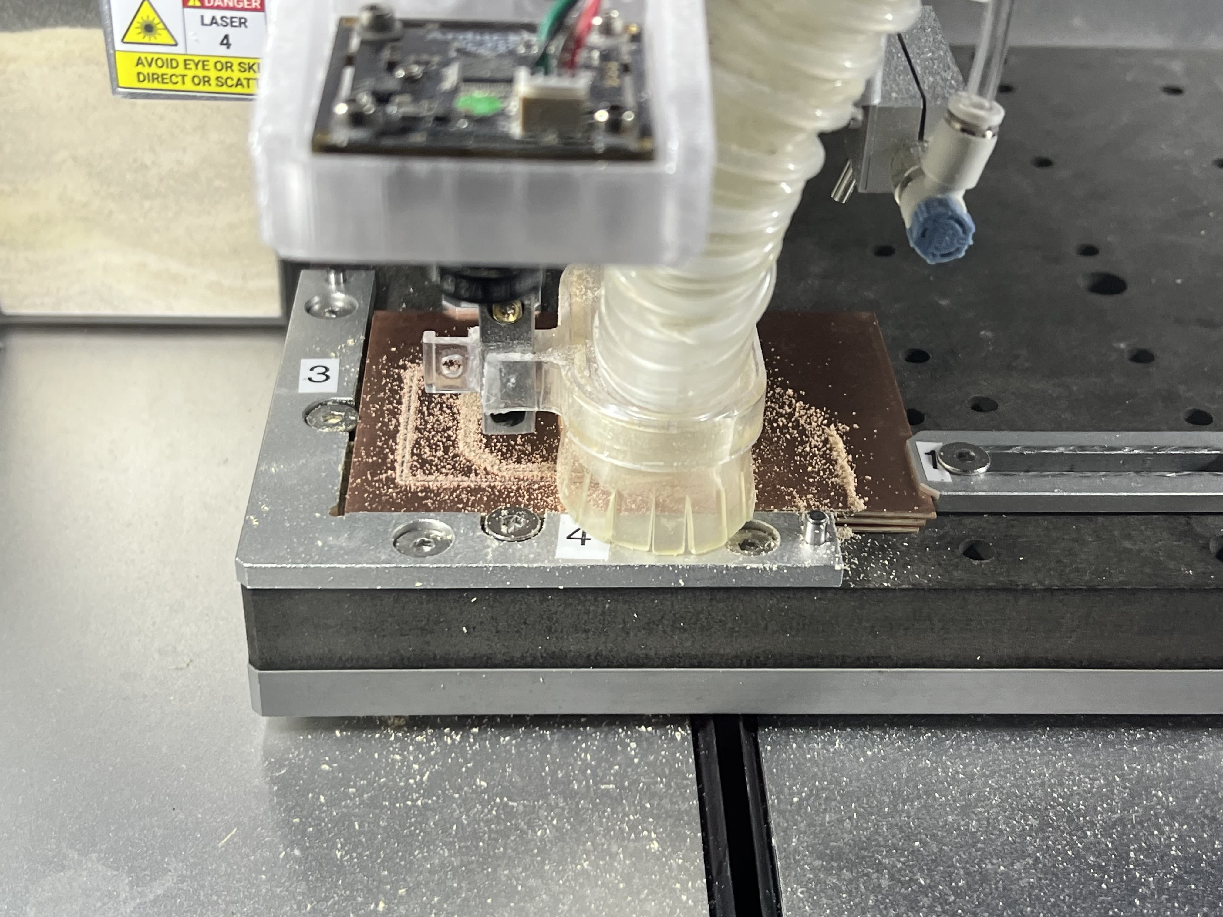
The CNC mill removing copper to create circuit traces
Watching the milling process is both fascinating and nerve-wracking. The tiny end mill spins at high RPM (typically 10,000-20,000) as it precisely follows the toolpath, removing copper in a fine dust. The trace milling pass removes the copper between circuit traces, isolating each conductor. For my design, this took about 15 minutes as the mill carefully navigated around all the pads and traces.
After the traces were milled, the machine switched to the outline cutting operation. This uses a larger tool (typically 1/32") to cut through the entire board thickness, defining the board shape. The tabs remain connected at this stage, holding the board firmly in place until the process is complete. Once milling finished, I carefully snapped the tabs to remove the board, then used a file to clean up the tab remnants and deburr the edges.
Final Results
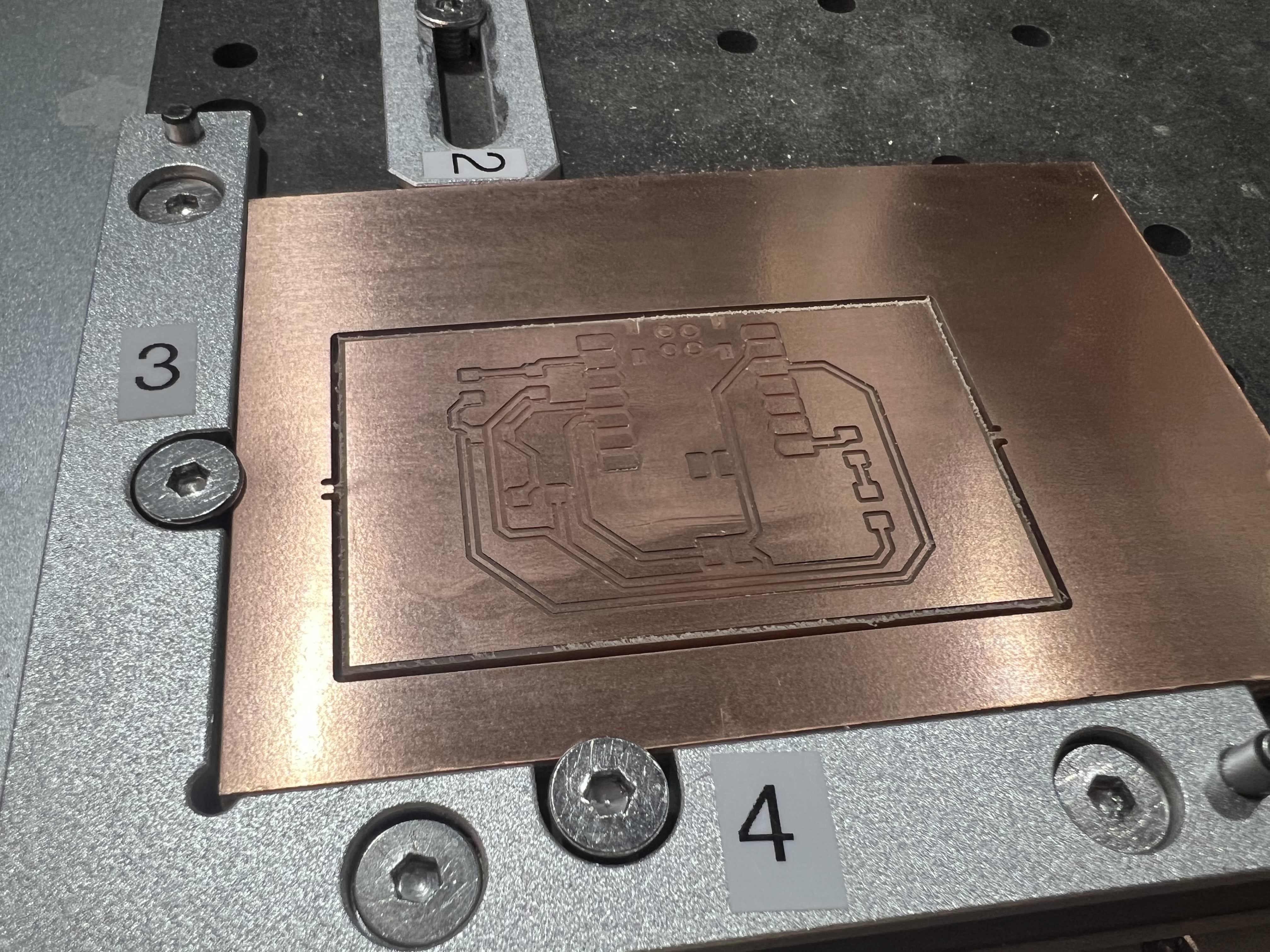
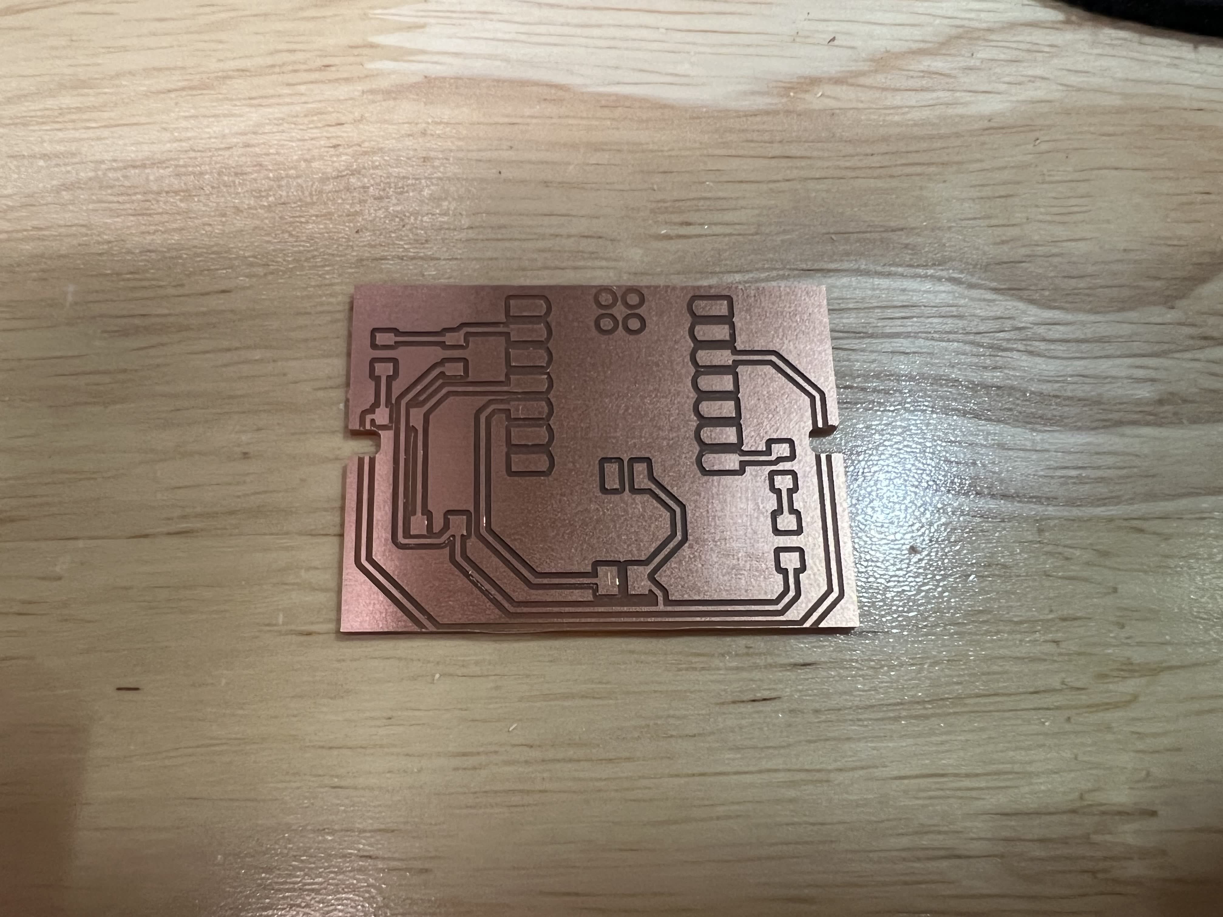
Close-up showing the quality of the milled traces
The final milled PCB exceeded my expectations. The traces were clean and well-defined, with no shorts between adjacent conductors. The pads were smooth and ready for soldering. The board outline was cut cleanly, and after removing the tabs and light deburring, the edges were neat. The larger edge cut boundary I had implemented in the revised design worked perfectly - the tabs had left no marks on the actual circuit area.
Inspecting the board under magnification revealed the precision of modern CNC milling. The 1/64" end mill had created traces and gaps that were consistent and accurate across the entire board. The copper removal was complete, exposing the FR4 substrate material between traces. All the component pads retained their full size and shape, ready to accept components during assembly.
Key Learnings from Production
Design for Manufacturing (DFM)
This project reinforced that designing for manufacturing requires thinking beyond just electrical functionality. The tab intrusion issue was a perfect example - the circuit was electrically correct, but the physical production process needed additional consideration. Leaving adequate margins, understanding how the board will be held during cutting, and planning for the complete fabrication workflow are all essential parts of successful PCB design. These DFM principles apply whether you're milling boards in-house or sending them to a commercial fabrication service.
Toolpath Verification
The toolpath visualization step saved me from a failed milling attempt. By catching the edge cut problem before committing to physical fabrication, I avoided wasting materials and time. This verification step should never be skipped - it's much easier to fix design issues in software than to deal with a poorly milled board. The few minutes spent reviewing the toolpath visualization can prevent hours of rework.
Machine Setup Precision
Successful PCB milling depends heavily on precise machine setup. The quality of fixturing (how the board is held), the accuracy of zeroing (especially Z-height), and the condition of the cutting tools all directly impact results. Small details matter - even dust or debris under the board can cause height variations that ruin the milling. Taking time to properly prepare and configure the machine pays off in reliable, high-quality results.
Technical Specifications
| Parameter | Value | Notes |
|---|---|---|
| Trace End Mill | 1/64" (~0.4mm) | Fine detail for circuit traces |
| Outline End Mill | 1/32" (~0.8mm) | Cutting through full board thickness |
| Spindle Speed | 10,000-15,000 RPM | High speed for clean copper cutting |
| Feed Rate (Traces) | ~4 mm/s | Balance between speed and quality |
| Cut Depth (Traces) | ~0.1mm | Just through copper layer |
| Cut Depth (Outline) | ~1.7mm | Through 1.6mm FR4 board |
| Board Material | FR4, 1oz copper | Standard PCB substrate |
| Total Milling Time | ~20 minutes | Traces + outline cutting |
Commercial PCB Fabrication
While in-house PCB milling is excellent for rapid prototyping and learning, I also explored the option of submitting the design to a commercial board house. This comparison helps understand the trade-offs between different fabrication methods - speed vs. cost, capability vs. accessibility, and learning value vs. production quality.
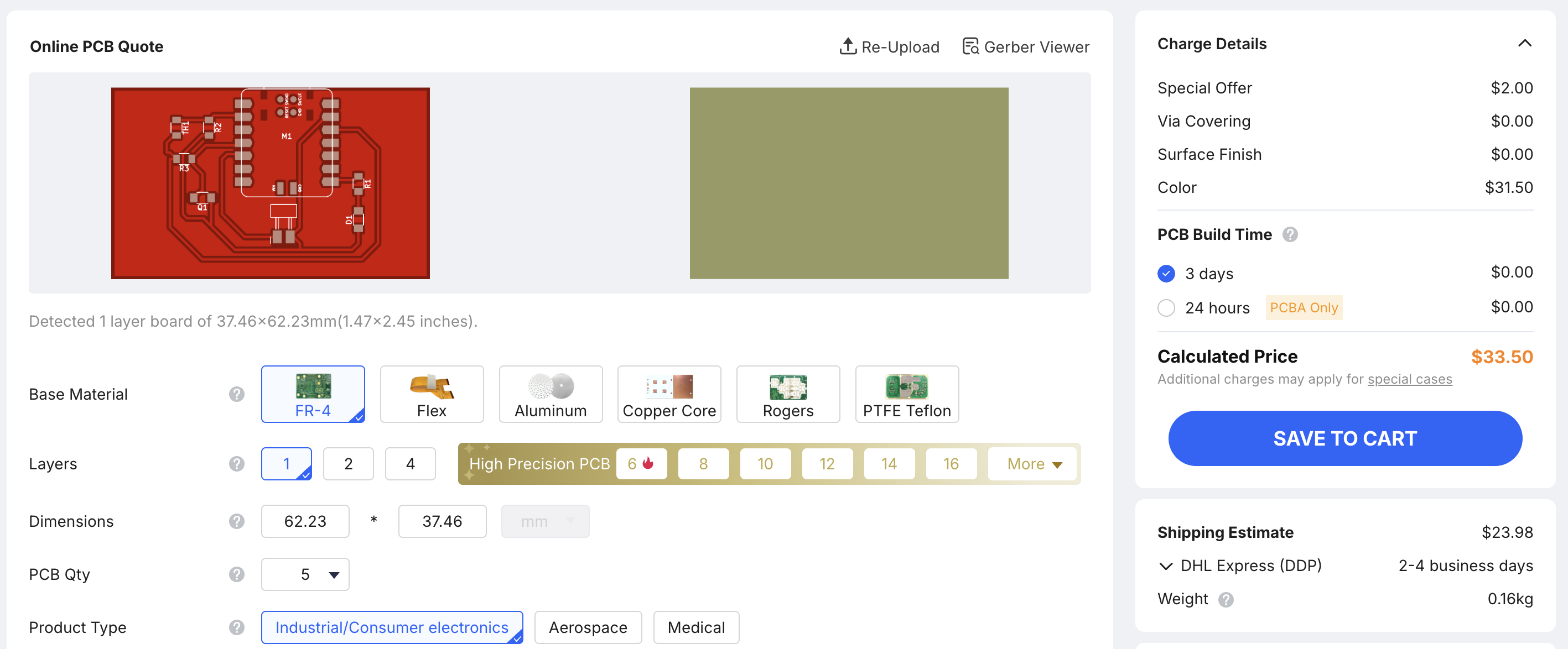
JLCPCB manufacturing quote: 5 pieces in red for approximately $33.50
Commercial vs. In-House Comparison
JLCPCB quoted approximately $33.50 for 5 PCBs with red solder mask. This commercial option offers several advantages over in-house milling: professionally applied silkscreen, plated through-holes for reliable vias, consistent copper thickness and adhesion, and HASL or ENIG surface finish for excellent solderability.
However, the in-house milling approach has its own benefits. The turnaround time is measured in ~10 minutes rather than days. There's no minimum order quantity or shipping delays, making it ideal for iterative design. Most importantly, the hands-on experience of fabricating the board provides deep understanding of PCB manufacturing constraints and design-for-manufacturing principles.
For this project, in-house milling was the right choice for learning and rapid iteration. For a production run or a design that needs plated vias, commercial fabrication would be more appropriate. Understanding both options and when to use each is an important part of electronics design workflow.
Next Steps: Assembly
With the PCB successfully fabricated, the next phase will be component assembly. This involves soldering all the components onto the board - the XIAO-RP2040 microcontroller, the phototransistor and thermistor sensors, the LED, speaker driver circuit, and all the supporting resistors and capacitors. The quality of the milled board provides an excellent foundation for assembly, with clean pads that should make soldering straightforward. Once assembled and programmed, I'll be able to test whether the physical board performs as designed in simulation.