
Electronics Production
"A printed circuit board (PCB)...is a medium used to connect or "wire" components to one another in a circuit...Printed circuit boards are used in nearly all electronic products." -Wikipedia
Group Assignment
1. I worked with my group to learn how to mill a PCB board and solder.
Under the guidance of Shop Manager and Technical Instructor Jen O'Brien, I, along with a group of students in the Architecture section learned how to mill a PCB board (Fig. 1A). Jen walked us through all of the steps including launching the program on the computer, setting up the machine, using the vacuum to clean up, and so on. I learned a lot!

Fig. 1A. Learning how to use the PCB milling machine.
As a group, we selected a test board to upload to the machine and mill (Fig. 1B). When the board was finished, we analyzed the pattern giving us an idea of the tolerances of the machine. We noticed that some of the very fine lines of copper peeled right off of the plastic layer underneath, meaning we have to design our PCBs appropriately to avoid this (i.e. using route thickness of at least 0.4 mm).

Fig. 1B. Test PCB.
Lastly, Jen taught us how to solder. This included an important lesson on keeping the Architecture shop neat, for example, only removing one drawer at a time to select a component and then putting the drawer back (Fig. 1C). After Jen collected all of the components she needed, she showed us how to secure them to a spare peice of cardboard, how to position the magnifying glass and light over the board, and use the soldering iron and solder to affix the components to the board.
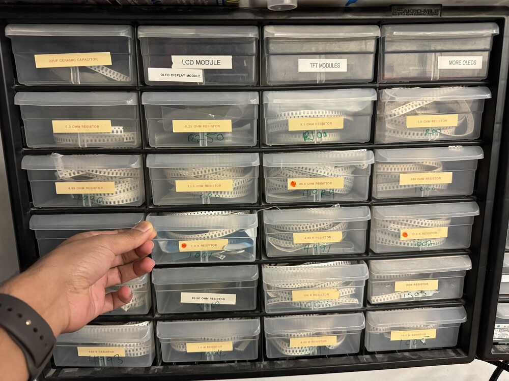
Fig. 1C. Important rule to keep organized.
There was a lot to learn this week, so I was excited to apply it all in the Individual Assignment!
Individual Assignment
2. I produced a PCB to simulate the functionality of my final project.
To make progress toward my final project, I produced a PCB with buttons and LEDs that simulate the operation of the gut machine. I started with a sketch of what I was trying to do: having 3 buttons operate 3 predefined programs involving outputs components (Fig. 2A). I attempted to do something similar in Week 05, but realized that initial attempt was missing ports for my output components. Ultimately, these outputs will be motorized air compressors/vacuums but as I did not have these components yet and might still have to make iterations on the board, I made a simple version with LEDs as the outputs (Fig. 2B).

Fig. 2A. Sketch of the final PCB and the program that the buttons control.
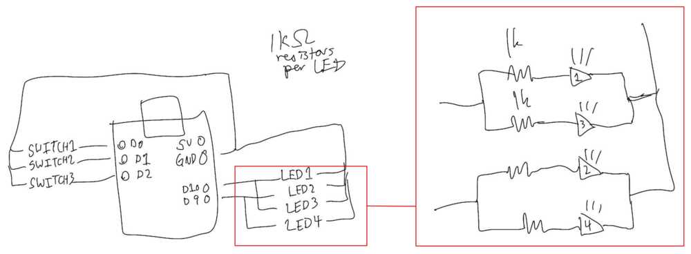
Fig. 2B. Sketch of the simplified PCB with LEDs.
I received help from Charlie Janson on my circuit design, including choice of resistors. I designed my board on Fusion 360 and then checked it over with Charlie, who pointed out I used the wrong LEDs (Fig. 2C).
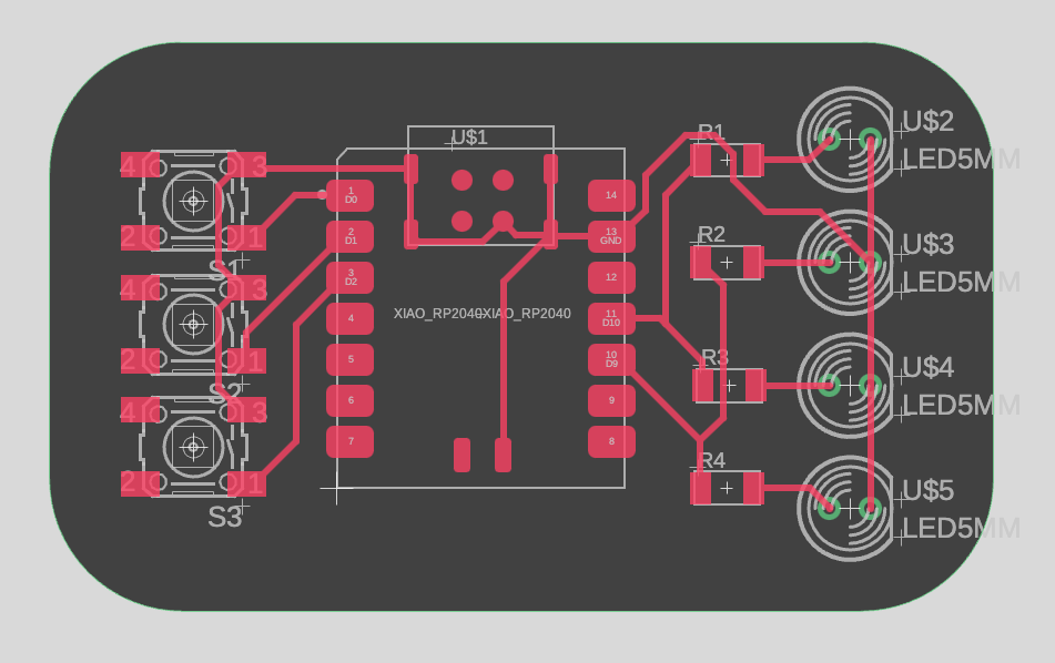
Fig. 2C. First iteration of the PCB layout.
As I learned in the previous week, designing a circuit is an iterative process! I went back to the circuit diagram and changed the LEDs to the correct components (Fig. 2D). After doing this, the PCB layout looked much better and more compact (Fig. 2E). The Fusion 360 file can be downloaded here. As a side note, I was a lot faster this week at designing the circut given my experience from the previous week, which was motivating.
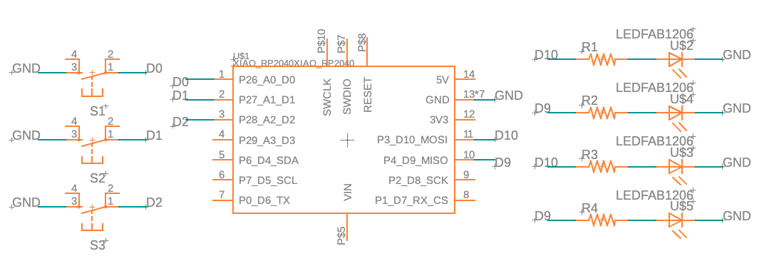
Fig. 2D. Final iteration of the circuit diagram.

Fig. 2E. Final iteration of the PCB layout.
When I had the final design, I exported it along with the outline as images (.png files) that I could send to the PCB milling machine (Fig. 2F).
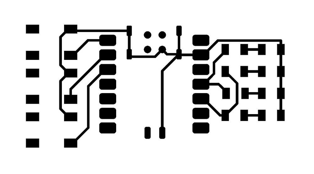
Fig. 2F. Image of PCB layout.
Charlie again provided his assistance in helping me set up the PCB milling machine, inserting the tool, opening up the mods program, and setting the toolpath to the origin to start the mill (Fig. 2G). Sending the file to the device began the milling, which seemed to start off smoothly (Fig. 2H).

Fig. 2G. Setting up the PCB milling machine through the mods program.
Fig. 2H. Milling the PCB layout.
After the milling finished, I used the vacuum to clean the board, making sure to leave it in place so we could start milling the outline from the same origin point. We uploaded the image of the outline (after editing it in Photoshop to fill in the background) and sent it to the device. However, when the milling finished, we realized the outline must not have been able to calculate the path properly as it was only partially milled (Fig. 2I).

Fig. 2I. Accidental partial milling of the outline.
Thinking I would have to restart the whole milling process, I asked Charlie what to do. He suggested we could manually cut the board on the band saw. Thinking of an alternative, I suggested inverting the imaging and recalculating the path in mods (Fig. 2J). This was the second edit we had to make to the exported outline image but I figured it would be worth a shot (Fig. 2K).

Fig. 2J. Inverting the outline image in mods.
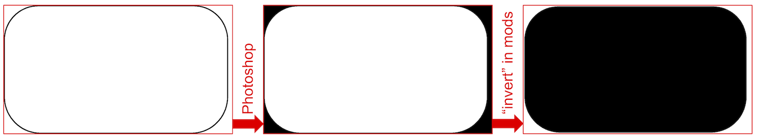
Fig. 2K. Workflow of editing the outline image.
It worked (Fig. 2L)! Luckily there was enough of a margin between the PCB layout and the outline as the new outline cut within the borders of the previous outline. I then removed the board and washed it with abrasive Gojo soap, preparing for soldering (Fig. 2M).
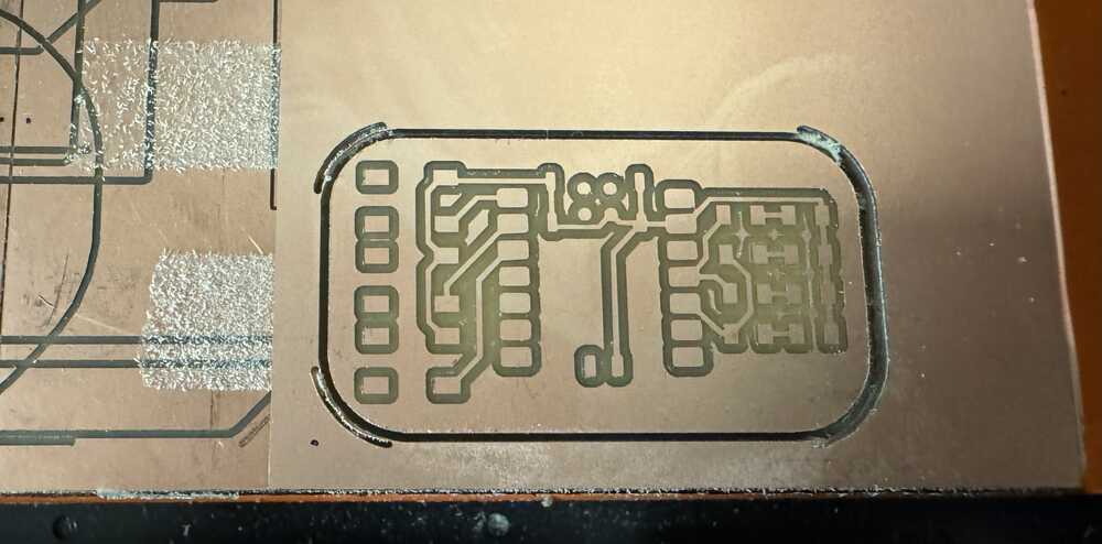
Fig. 2L. Image editing of the outline.

Fig. 2M. Cleaning the PCB.
After cleaning the board I secured it with double-sided tape to a spare peice of cardboard along with the components I would be soldering (Fig. 2N). I then placed the cardboard under the magnifying glass and began soldering the components, starting with the buttons (Fig. 2O).
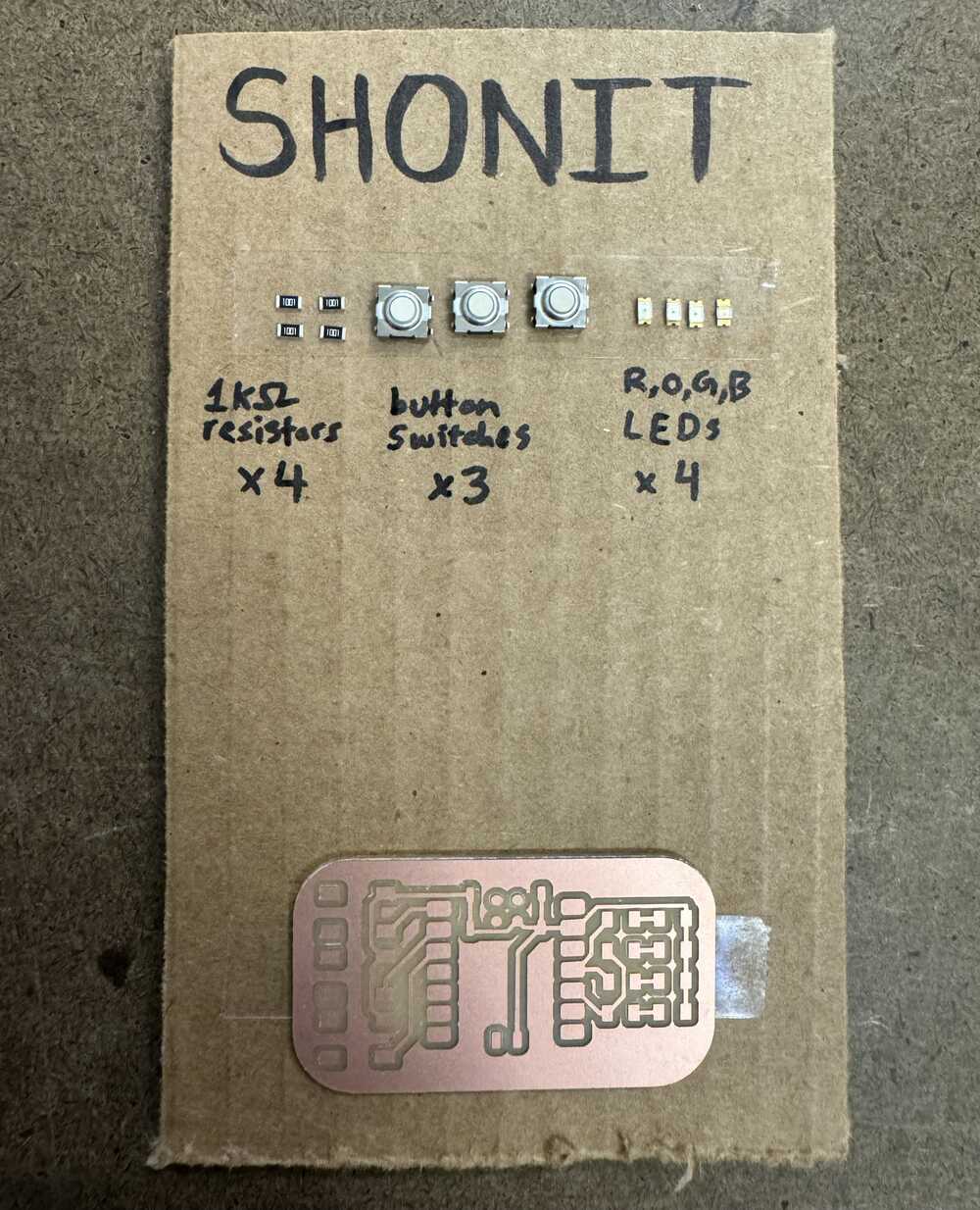
Fig. 2N. Keeping my components organized.
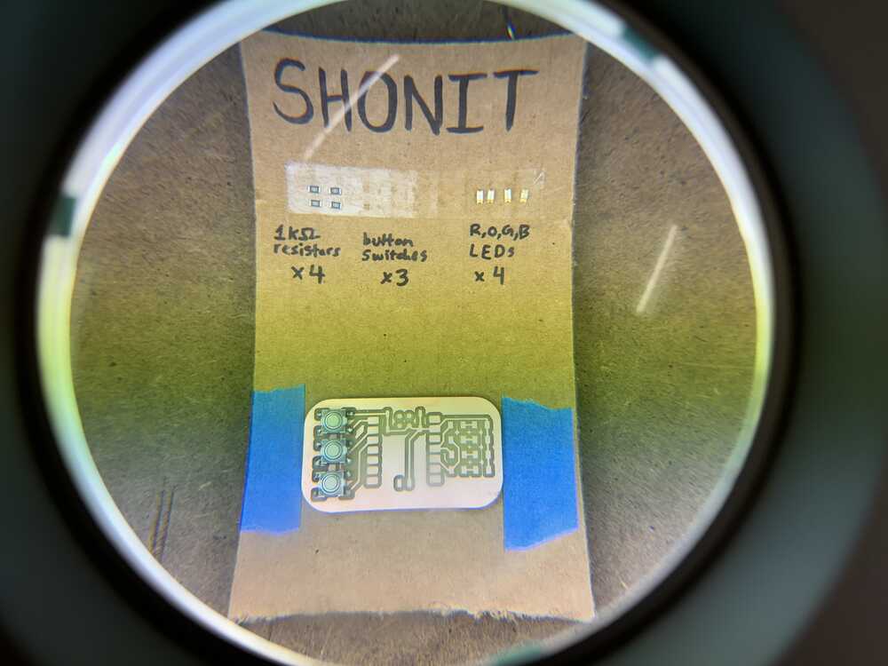
Fig. 2O. Began soldering the buttons under the magnifying glass.
I learned how to solder a few years ago, but have not practiced since then. I was very rusty, spending a few hours to solder the 12 components to the PCB (Fig. 2P). However, I could definitely see myself getting better as the time went on. The buttons probably took 1 hour to solder, the microcontroller 30 minutes, the resistors 20 minutes, and the LEDs 10 minutes.

Fig. 2P. Soldered PCB.
For sake of time this week, I wrote a code to test the functionality of the LEDs (Fig. 2Q). Each LED lit up according to the code, indicating the soldering was successful. Preliminary testing of the buttons was unsuccessful, but I will return to this in Week 09 when I work on Input Devices.
Fig. 2Q. Testing the LEDs.
This week's assigment was the one that required the most time so far. It required me to pull from my toolbox of skills from Week 03 and Week 05, in addition to learning and implementing new skills for the week. Though it was a lot of work, it was a great learning experience in electronics and allowed me to think more about my final project and how to make it!