electronics design
This week I built the baseline hello-FTDI board, with a green LED and tactile switch connected to the PB2 and PA7 pins of the ATtiny44A. I programmed it with the hello-echo AVR code, as well as a simple button-blink program. I used parts of this tutorial. It all worked out fine.
design in Eagle
I spent most of my time working through the Eagle user interface. When a UI is really terrible it means there's probably a useful scripting interface to the tool. Nevertheless, because of the simplicity of the board, I decided not to invest heavily in learning all the Eagle commands that would probably make things easy.
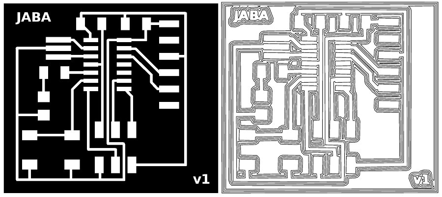
schematic
Producing the schematic was fairly straightforward. I used net naming to connect signals, which kept the diagram very neat.
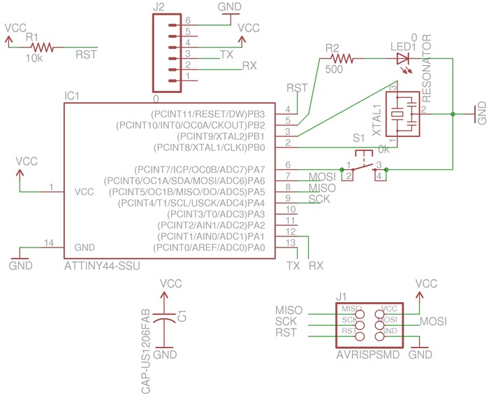
My biggest problem was finding the right library parts, which took many iterations. I got by using a few strategies: (1) using wildcarding when searching for parts in the Add dialogue (e.g. *switch*), (2) matching the library part's footprint with the actual inventory part's datasheet on DigiKey, and (3) just knowing which library parts I needed by word-of-mouth.
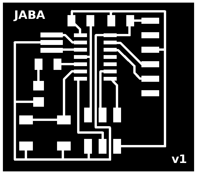
board
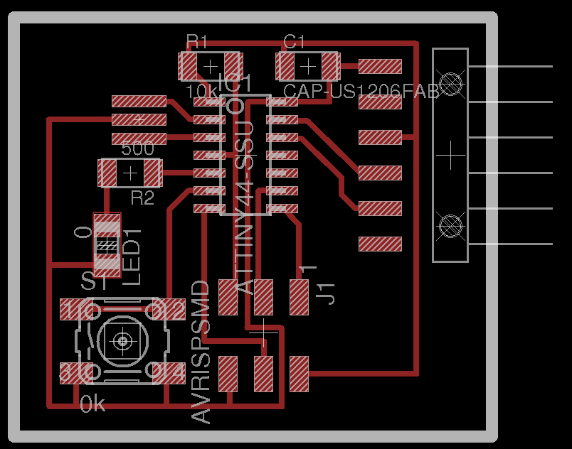
In board mode, I moved the components into the same configuration as the hello-FTDI board and put the LED and button in the negative space under the resonator. I placed/oriented the LED and button so their traces wouldn't overlap.
Following suggestions from the mailing list I setup a placement grid (View->Grid) at 25mils and snapped component placements (File->Run->cmd_snap_board.ulp). I then used Eagle's autorouter to lay down 15mil-wide traces in the (1) Top layer. I found that setting the track width of the Route tool (below) didn't affect the autorouter's track width.

Instead, I had to edit the track width setting of the default net class in Edit->Net Classes. The autorouter results were decent, but I went ahead and made my own adjustments. The RIPUP command was very useful in board mode, since you can't undo the autoroute command ("RIPUP *" clears all the routing). I used the DRC-check tool to make sure there weren't any problems. The final version of my board:
milling
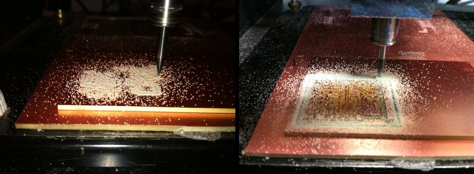
When I converted my first pass at the board layout into milling paths, I found that there were a few areas of concern.
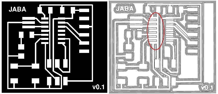
Mainly, the entire length of the reset signal that travels underneath the ATtiny was shorted with a number of its pins. Even though Eagle's DRC check didn't say anything, the 1/64" endmill's multiple passes mean you need more space between tracks and pads. Rather than fiddling with milling settings, I went back and reworked a number of paths.
I then milled the traces and cut the board out using a 20px border created in GIMP.
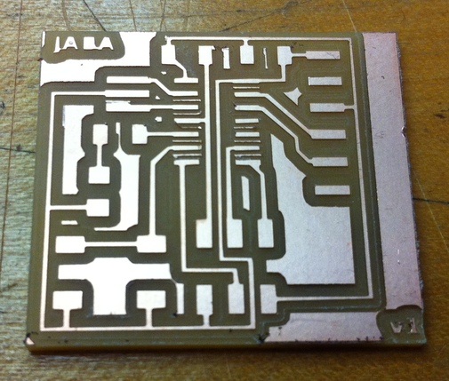
The board after milling and deburring:
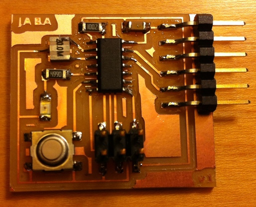
stuffing
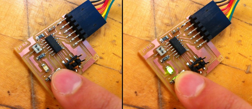
Stuffing went fine. Soldering skills still aren't great, but starting to get the hang of it (3 hours on the fabISP down to 1.5 hours). One note was getting the orientation of the button correct: there are lines on the bottom of the button indicating the pairs of connected pins.
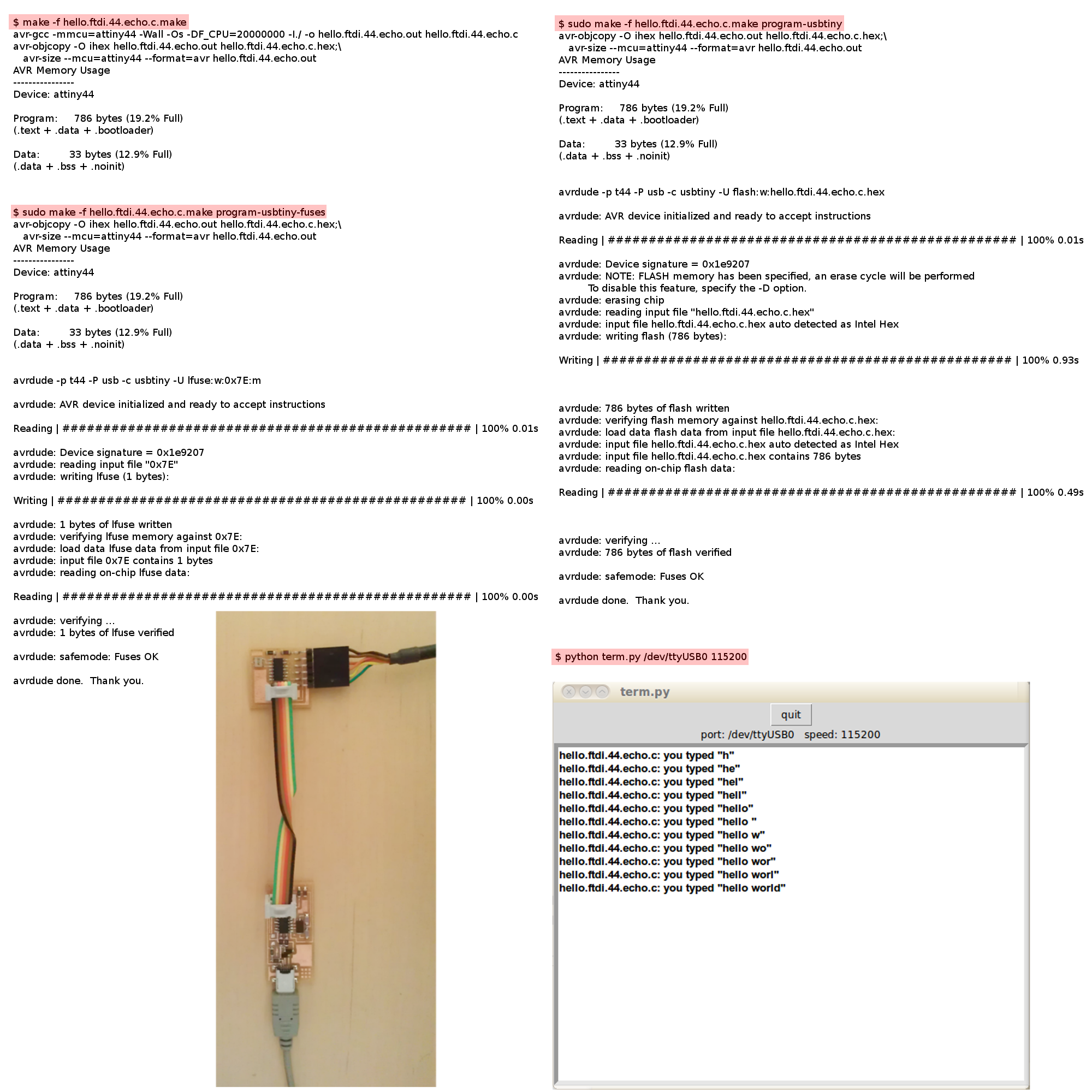
programming
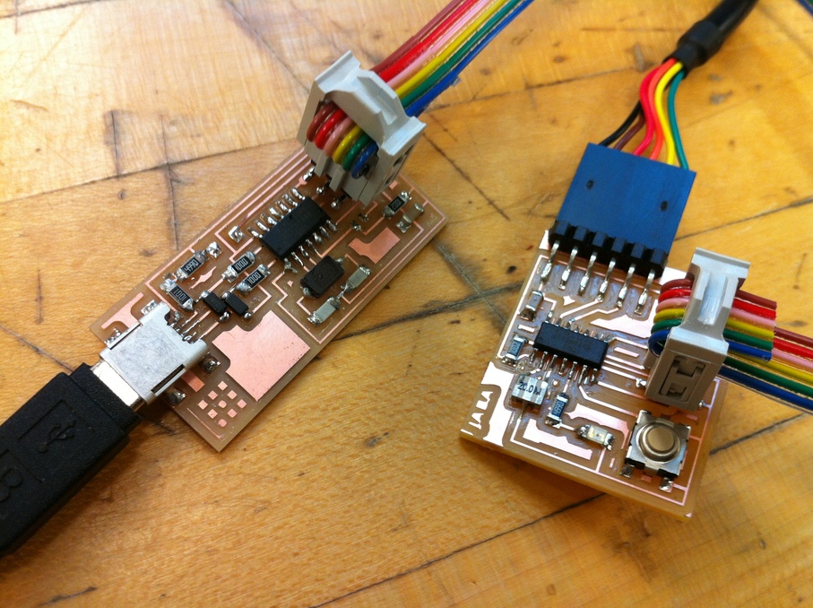
I first made a fabulous rainbow cable to connect my fabISP to the new board, following Jin Joo's tutorial. I followed these instructions to compile the hello echo program, program it onto the board, and run it using Neil's term.py script.
It wasn't working at first, but then I realized I had the FTDI connector plugged in upside-down. Make sure the black (GND) and red (VCC) cables are connected to the right pins on your FTDI header!
I tested out the button and LED part of my board using a slightly-modified version of Kelly Shaw's blink program. Can't believe those tiny traces are doing their job. Looking forward to building something more interesting.
Quick explanation of the code, so people with different pin arrangements can adjust accordingly. There are three types of 'registers' for dealing with inputs and outputs of the ATtiny44A: DDRA/DDRB, PINA/PINB and PORTA/PORTB. The DDR (Data Direction Register) stores whether pins are input or output pins - writing _BV(PB2) to DDRB indicates that PB2 is an output pin. The PIN register can be used to read/input signals from the pins - PINA & _BV(PA7) reads the value of PA7, for example. The PORT register is used to write/output data on output pins - writing _BV(PB2) to PORTB sends a 1 (high signal) to PB2. If your program isn't working, make sure you're using the correct register (for example, PORTA for PA* ports and PORTB for PB* ports).
            // LED Button Blink Program
            //Button is on PA7
            //LED is PB2

            PORTA= _BV(PA7); //Turn button pullup resistor on
            DDRB = _BV(PB2); //Enable output on the LED pin
            PORTB = _BV(PB2); //Turns LED on

            //LOOP
            while (TRUE) {
              //button is not pushed
              if ((PINA & _BV(PA7))) {
                PORTB = 0; //turn LED off
              //else, turn LED on
              } else {
                PORTB = _BV(PB2);
              }
            }