Week 10: Input Devices
This week’s assignment is to "measure something: add a sensor to a microcontroller board that you've designed and read it."
In order to free up some time for my research and for my final project I decided to design and build my
Second Nature final project, as it’s an input device.
Objective and basic principles
Objective: To get a qualitative measurement of the number of insects that are present in the perimeter of the bug counter (insects can be indicators of an ecosystem’s health) Basic principles:
- Many nocturnal insects are attracted to light
- Why? Because they use the moonlight to navigate.
- They are attracted to Blue and UV
- Most of them are blind to the Yellow, Orange and Red part of the spectrum
- We can use blue light to attract insects in the counter
- We can use red light to measure their presence and quantity
The Bug Counter – Overview
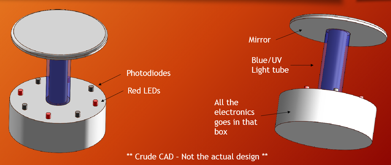
High-level implementation:
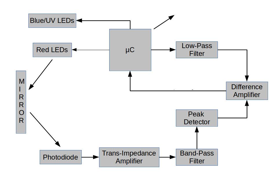
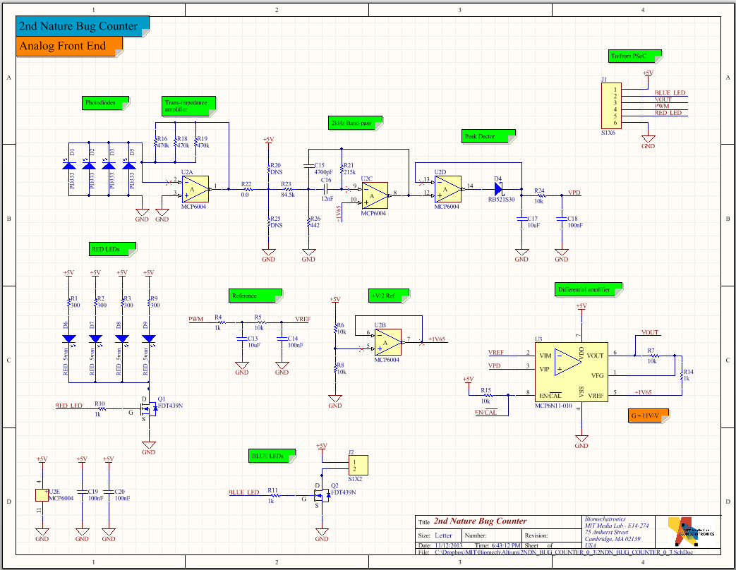
Implementation: the analog front-end (AFE)
From the electronics flowchart one can guess that I’ll be measuring really small analog voltages mixed with a lot of noise (other light sources). It’s
not possible to do all the signal conditioning with digital electronics (at least not with the sensitivity and resolution I need). I need analog
electronics to filter my signal and to extract useful information from it.
Let’s detail some of the sub circuits.
Photodiodes and trans-impedance amplifier
![]()
A trans-impedance amplifier is a current to voltage converter that uses an operational amplifier (http://en.wikipedia.org/wiki/Current-to-voltage_converter).
It transforms the photodiode’s current in a voltage. I used 3 resistors in parallel to be able to easily modify the gain of this stage. Without a red filter
(optical filter) this stage can easily get saturated.
I’m placing the 4 photodiodes in parallel to add their currents. It’s a simple way of getting a larger sensing area.
Band-pass Filter
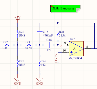
The North-American power grid works at 60Hz. There is a lot of electrical noise at 60 and 120Hz (rectified 60Hz). Incandescent lamps are also modulated
by that frequency: it can introduce noise in my system. Can I use a simple high-pass filter and be done? No, because fluorescent lamps work in the tens
of kilohertz.
I arbitrarily decided to do my measurements at 2kHz as it’s far enough from 60Hz and 20kHz. While this system is made to be used outdoors, having the
ability to take clean measurements in a lab is essential for the debugging and testing.
The bandpass filter was designed with Filter Lab. It passes signals from 1.8 to 2.2kHz. The +1V65 net name on pin 10 of U2 is a mistake, it should read
+2V5 (I was initially using 3.3V, 3.3V/2 = 1.65V). The idea is that my sinusoidal signal is centered at mid-supply.
Peak Detector

It’s possible to make a peak detector with only a diode and a capacitor. However, with low-voltage electronics the voltage drop of that diode can eat
up a significant part of the signal. As I had a free op amp in my quad package I decided to use it to build an "ideal" peak detector.
That circuit transforms my sine wave in a somehow stable DC voltage. R24 and C18 form a passive low-pass filter (fc = 159Hz) that rejects a good part
of the 2kHz noise from the signal. The signal named VPD is a DC voltage that’s proportional to the amount of light that is measured by the photodiodes.
Reference voltage
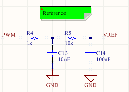
From the previous paragraph one could think that measuring VPD would solve my problem. More bugs equal less current equal less voltage, perfect.
However, the variation from a single insect could hardly be measured.
To fix that issue, I want to amplify not the VPD signal itself but the difference between VPD when there is no bug and VPD when moths are flying
around my sensor. To do that, I’m using a microcontroller.
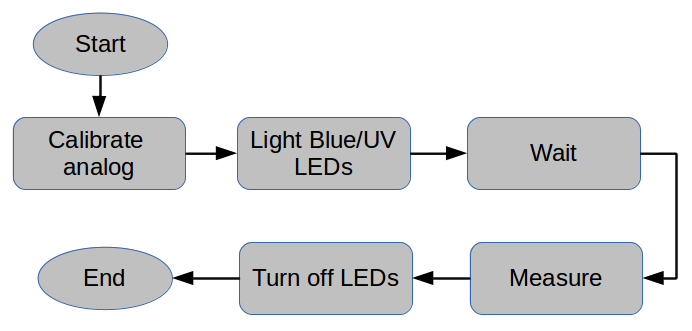
On the Software flow chart there is a block called "Calibrate Analog". What that means is that before turning the Blue LED on (we assume that no
light means no insects, or very few) the µC will adjust the PWM duty cycle to get a reference voltage (VREF) as close to VPD as possible. When the
2 are equal, the output voltage will be centered at mid-supply.
Differential amplifier
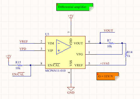
Now that we have VREF ~= VPD, we can turn the Blue LEDs on and attract bugs. The MCP6N11 will amplify the difference and the µC will read this
signal. For now the gain is really low (G=11). It’s enough to give me a clean detection when I place the tip of my tweezers in the light path!
Building the first circuit
I started by designing the analog front-end and a variation of my PSoC 4 dev board on the same PCB. I designed the whole thing in Altium and made sure
that it could be made on the Modela.
My initial plan was to use a 10 mil end mill because in the past I got good results from it. I started the job Saturday afternoon. After 40 minutes of
milling the top traces the end mill broke… it was my only one and the bin was empty.
I went up to my office and modified my land patterns to accommodate a 1/64th end mill. Generated the files, started the job. After half an hour the
end mill got loose and started jumping around. A second scrap PCB! It seems that one of the set screws of that Modela has bad threads. When you run
a long job the mill gets loose. That’s probably what killed my first one.
At this point I was annoyed. I decided to modify my files to build only the analog front end for now as it was the part with the most unknowns. I
milled it with the other Modela. It’s a really simple single-sided board.
This consumed my whole Saturday. For the 3rd time of my life (once per different school) I abandoned all hope to make decent circuits on a CNC mill.
I spent part of my Sunday experimenting with DIY methods of doing toner transfer and of etching PCBs without ferric chloride. With my super simple
setup I can get PCBs that are much better than what I could mill for a fraction of the time (and of the cost).
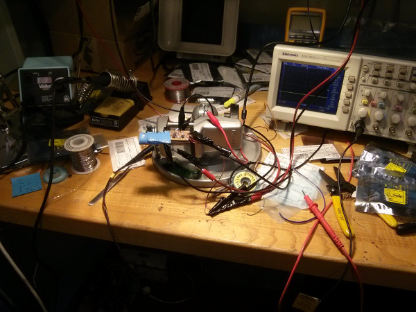
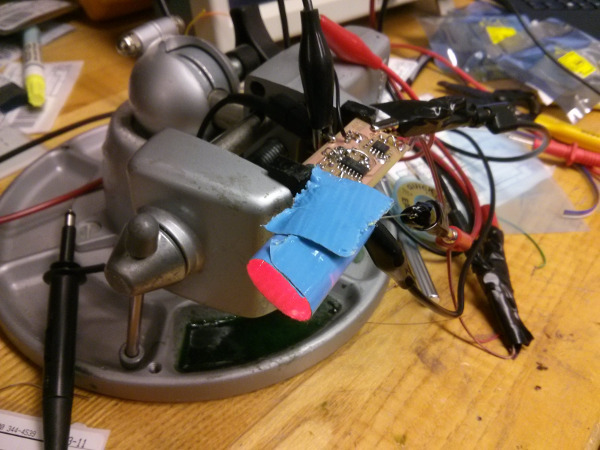
Testing the v0.2 circuit
I assembled the v0.2 circuit Sunday. That’s the "analog front-end only" PCB that I made on the Modela late Saturday. All the values that I selected for
my analog building blocks proved to be adequate. At the end of my test I could measure obstruction in the light path as small as the tip of my tweezers.
All the clocks were generated with function generators and the results were read by an oscilloscope.
Enclosure Design
Now that my AFE design is tested it’s time to build a housing for this sensor. I kept the same design principle as on the initial mock-up. I designed it
to be either 3D printed (for my prototype) or casted (for the future).
Here’s the actual design:
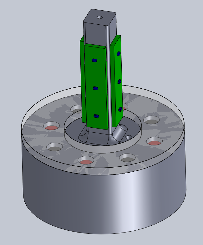
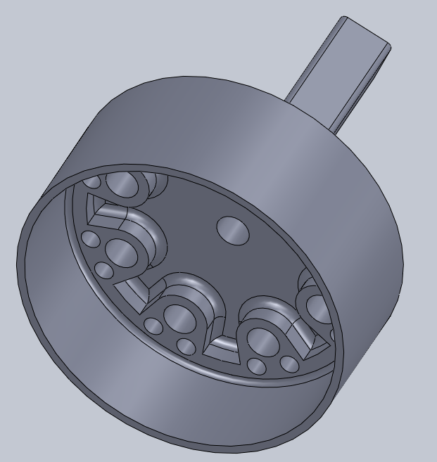
It’s currently being 3D printed.
PSoC 4 v0.3
As I said before, I removed the PSoC from the analog board. The idea was to use an external board, like the one I’ve used for my LED lamp.
I didn’t want to disassemble the lamp so I decided to build more boards. I made slight modifications to the design (3 LEDs instead of 8, new connector with 5x GPIO
& slightly smaller PCB (it's now possible to make 2 boards from a single 2x3 bare board)). Here’s the result:
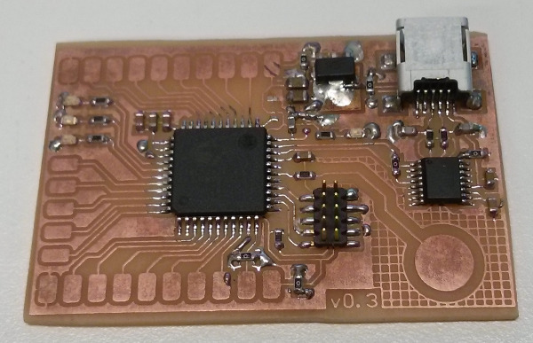
Building Circuit #3
The design of v0.3 is almost the same as for v0.2. I simply added more LEDs and photodiodes and a convenient connector with all the relevant signals. The board
shape was changed to fit in the mechanical enclosure.
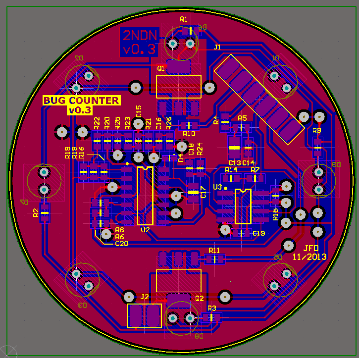

I rushed both the design and the assembly. You can see the effects of that on the quality of the circuit…
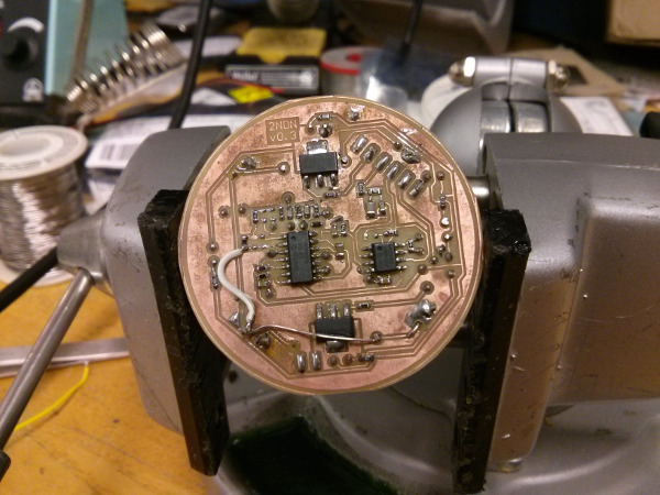
I successfully tested all the sub circuits. Only one small bug needs to be fixed (the half supply reference is lower than it should be). Next week I'll write the application software.


Jean-Francois (Jeff) Duval - jfduval(@)media(.)mit(.)edu - 2013
Top | MIT Media Lab | How To Make (almost) Anything 2013 | Index
"Hidden" keywords: Jean-François Duval, JFDuval, Jeff Duval, PCB, Dishpenser, MIT Media Lab, Biomechatronics, Electronics, Robotics, DIY, Hack, Hacker