Kim Smith
Electronics Design
Designing with Eagle
I thought this would be easier than it was…
first a super helpful recitation about electronics.
- Basic equations:
- V=IR
- Kirchhoff's current law (KCL): The sum of currents in a network of conductors meeting at a point is zero.
I started adding pieces onto a schematic in Eagle.
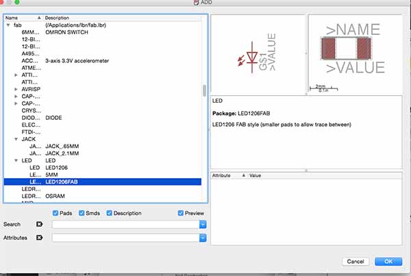
Edit--Add--then look up the part under the Fab library. Some things were more mysterious, such as ground (GND) and voltage (VCC)...they were in the Supply1 library in Eagle.
- Parts:
- fab/attiny44-ssu
- fab/res-us1206fab
- supply1/+5V
- supply1/gnd
- fab/resonator
- led/ledsmt1206
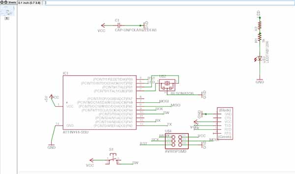
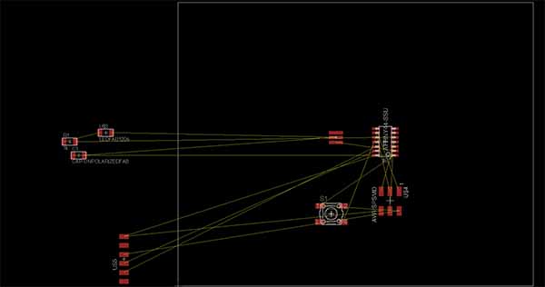
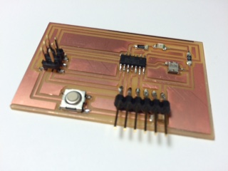
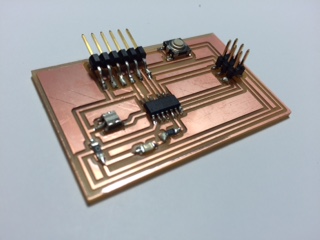
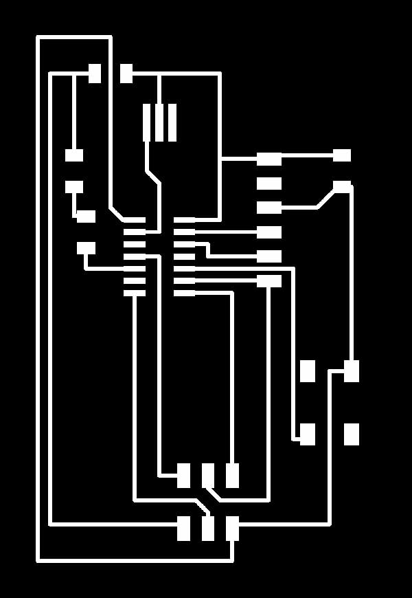
First placed the pieces on the boundary of the board and roughly tried to place them in an efficient orientation. Right click to rotate. From here is was a long confusing puzzle. But was fun. Trying to get the wires the most direct route, not crossing...I had some difficulty keeping it straight when I tried to clean up my initial design. I left my design bigger than it should have been. I realized later that it was even too wide for the copper plate. So, I shrunk it down to fit comfortably, although it probably could have been much more compact. In one spot I could not figure out how to route without crossing, so I inserted a zero ohm resistor to jump over. After I was happy with the layout, I hid extra layers so that only the routes and part footprints were visible. I exported to png file, saving it at 600dpi, in monochrome.
Milling
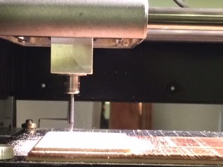
This process was the same as last time and this time it went very smoothly. I first loaded the settings and then walked through the fab module to set up the png for milling. I had some difficulty maintaining the connection between the computer and the Modela, which happened last time and I still am not sure how to trouble shoot that one. I managed to cut the board in one try with the traces; however, I had something wrong on the outline, because the first try didn't cut through the outline. I had drawn my outline in Photoshop, after having some difficulty getting a wide enough boundary in Eagle. I changed some settings, rebooted it all, and then cut again. It came out beautifully.

Stuffing
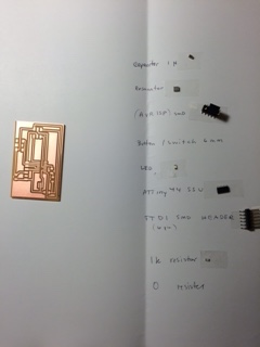
Again, this step was easier the second time around. I started by gathering all the parts and laying them out. Keeping organized and clean makes this part easier. Soldering was easier, but I am still struggling with getting the solder and flux the right temperatures to flow well. My joints looked cloudy after several tries...But, it came together.