Week 4: electronics design
Skills used: PCB (printed cicuit board) milling, soldering, and programming.
Part 1, Echo:
This week was tough, after several failed attempts I managed to mill an ATtiny412 (that dooesn't yet do much) and load "echo" onto the D11C milled for Week 02's assignment. This process was confusing to start. The first step was to download the library for KiCAD, and the corresponding footings by going to Preferences > Manage Symbol Libraries. This gives you a class library for developing the schematic and the necessary symbols when drafting the traces between components in the PCB Layout Editor. (Both the library and the footings for KiCAD can be found on GitLab under the issue tracker.) Once you have completed this step, KiCAD itself is rather easy to use. Zach provided a link to his friend's KiCAD tutorials, which can be found here.
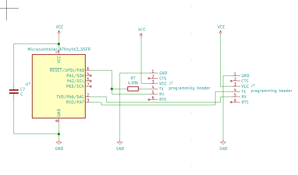
After navigating the schematic organization of the PCB, you need to process the wire connections and the profile cut in the PCB layout editor. I find this and soldering to be the most enjoyable part of the assignment.
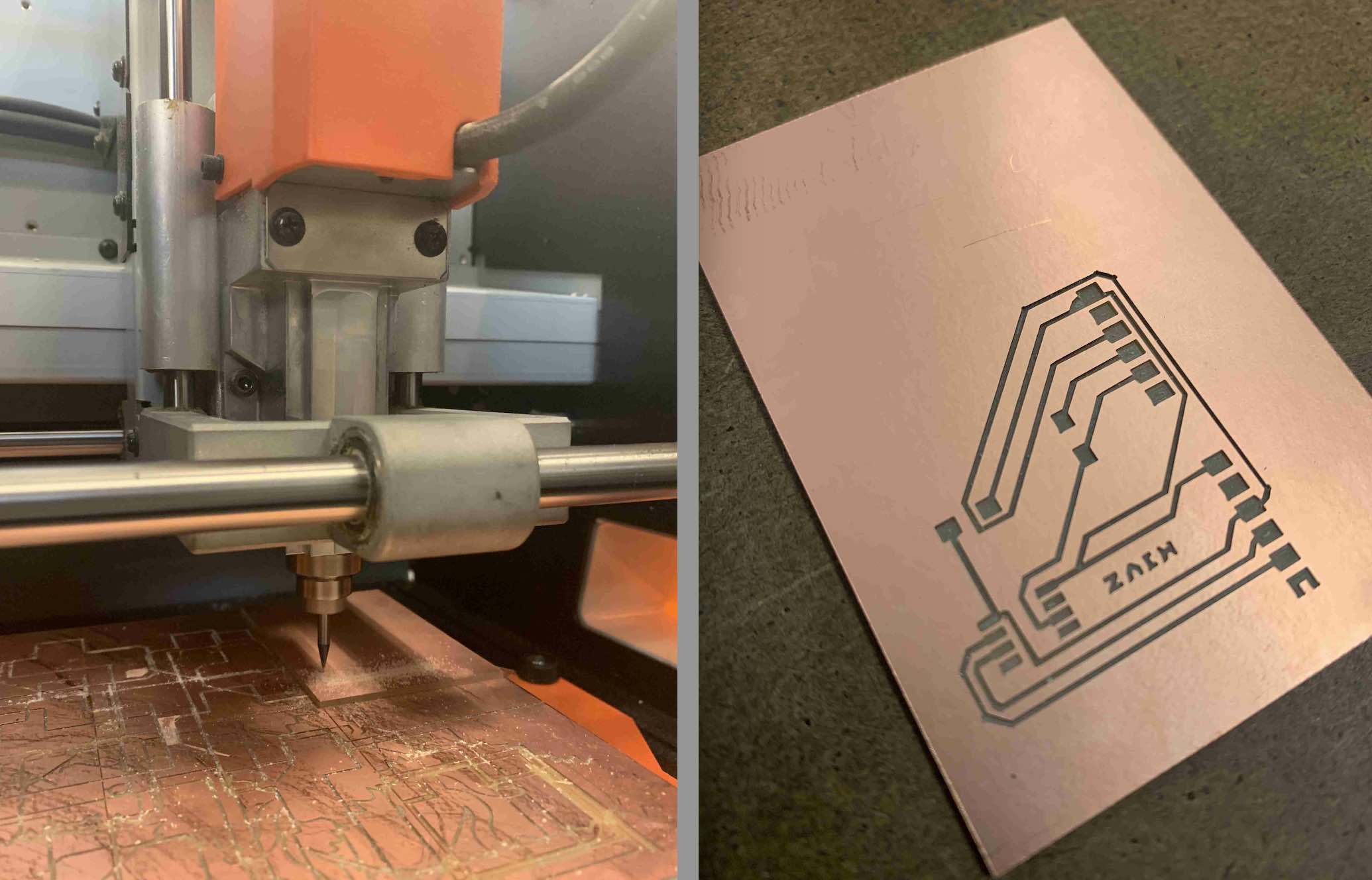
Once your traces are set in the PCB editor, you need to edit the exported copper traces and the board outline, I chose to use Illustrator. What is needed for MODs are two sperate files, one for the traces (which uses a 1/64 drill bit), and one for the outline (which uses a 1/32 drill bit).
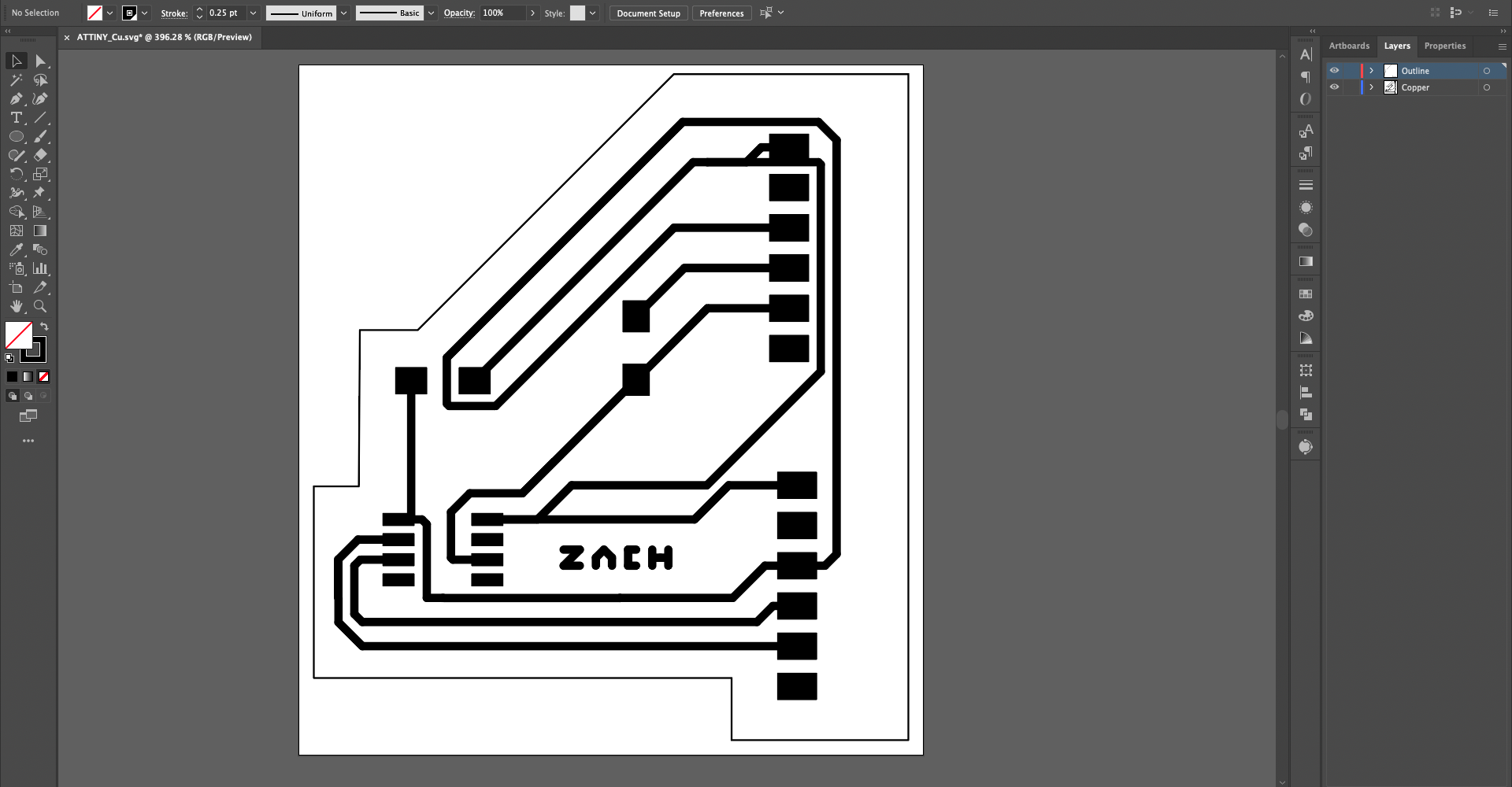
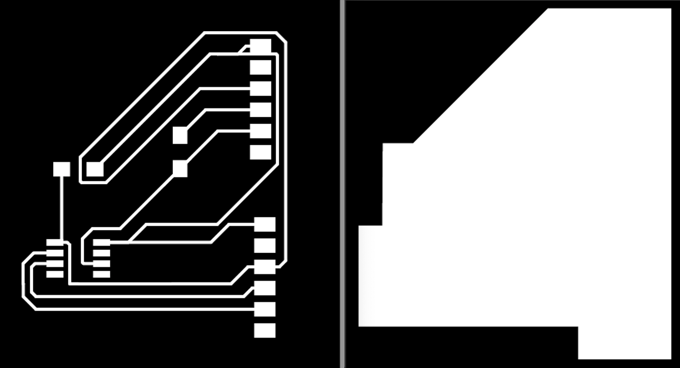
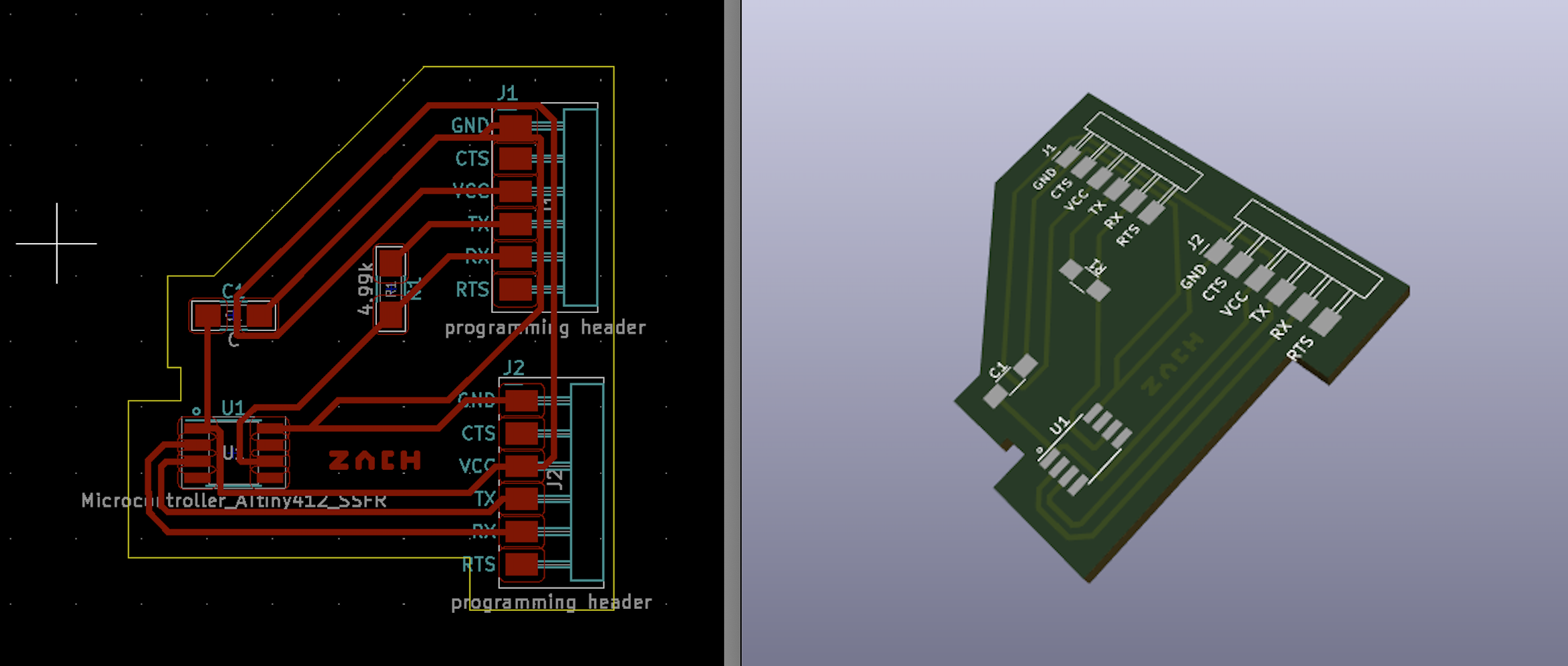
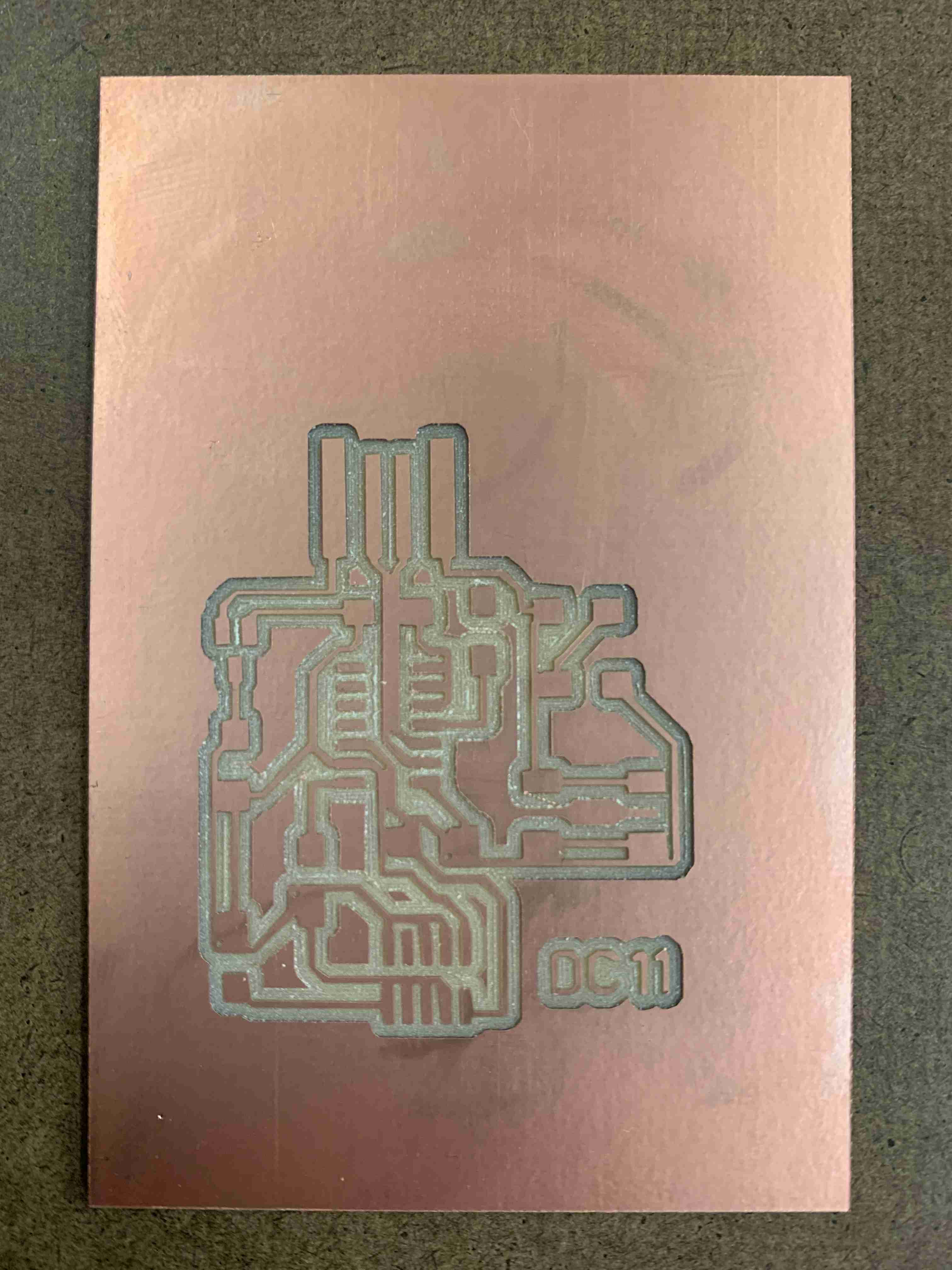
Afer you have exported the two files, you can mill your PCB. On my first pass, I exported a .svg from Illustrator, but found issues when loading the .svg into MODS for the Roland SRM-20. When re-exporting the file as a .png the Roland SRM-20 I had no issues… The only problem was, I needed to invert my .png. My first PCB, milled the traces rather than the space between them.
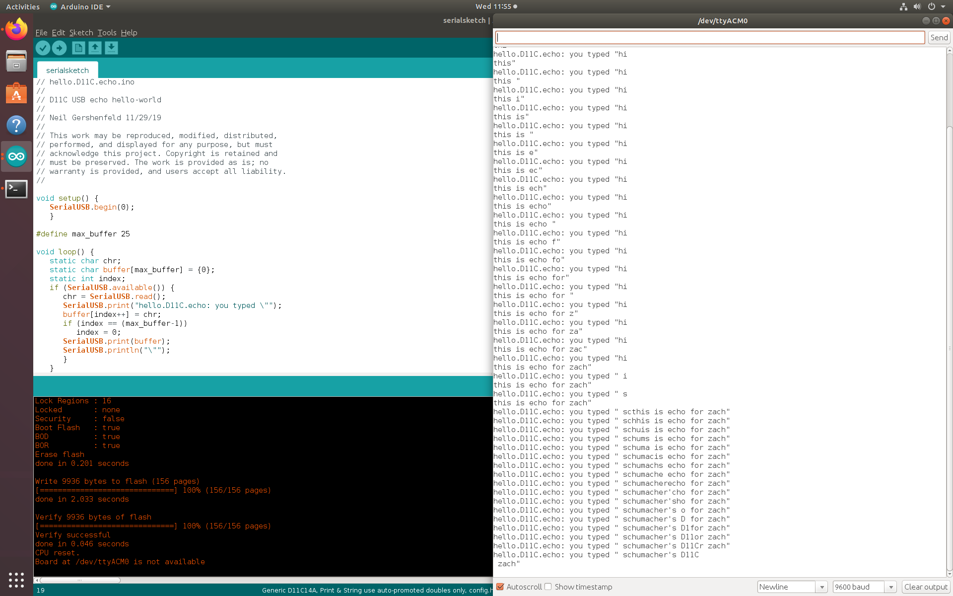
The board was then soldered with the neccessary bits to link to my USB microcontroller, and run the Echo program.
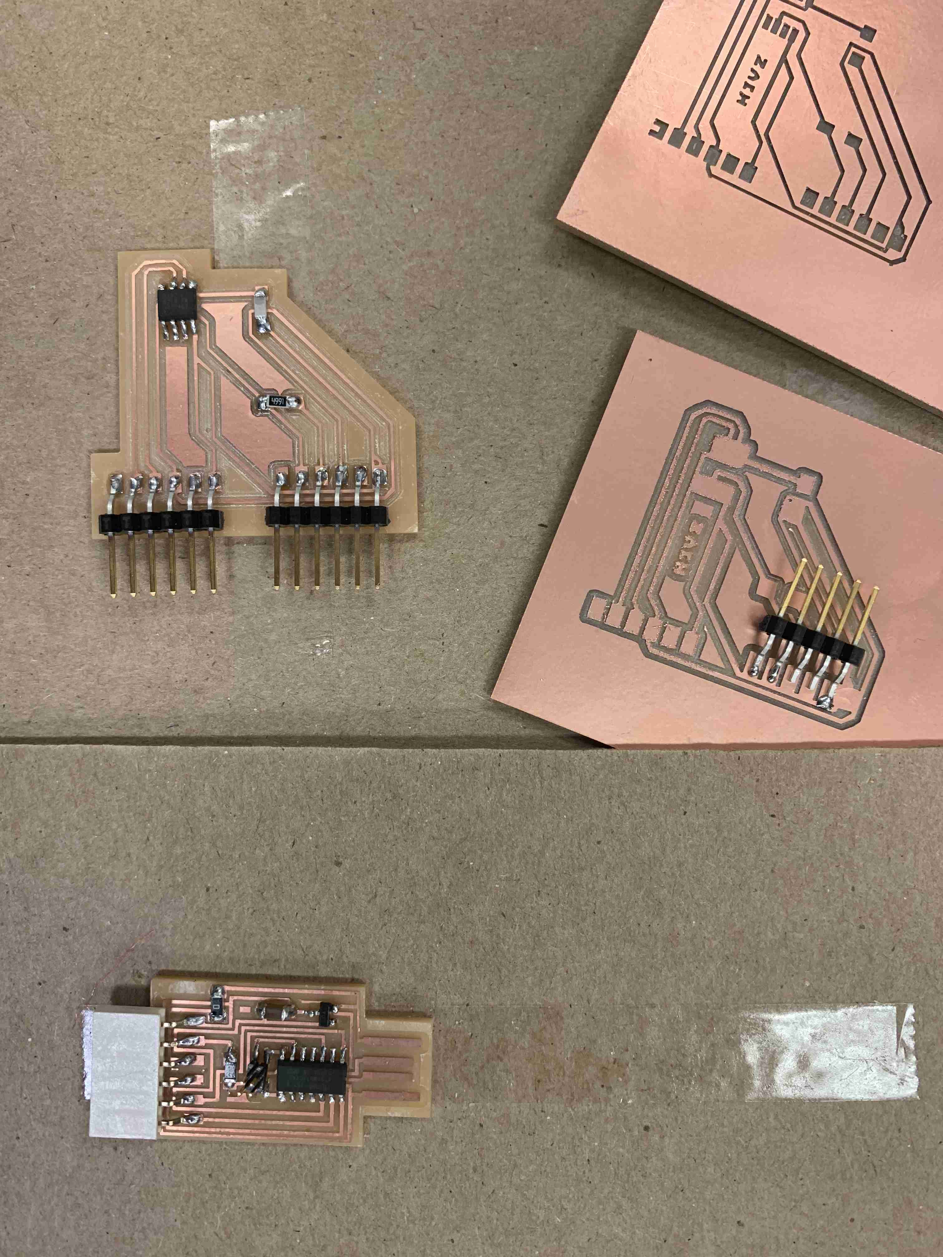

After bootloading the D11C, we ran the Echo command with the help of my classmates.

Part 2, LED Blink:
Repeating a similar process as above, I built upon the DC11C that was provided to us, and added a button and LED. Drafting this PCB was a challange at first. In order to properly connect this board's components on one single-sided face, you need to run multiple channels under parts, and in some cases add resistors (0) to bridge over channels.

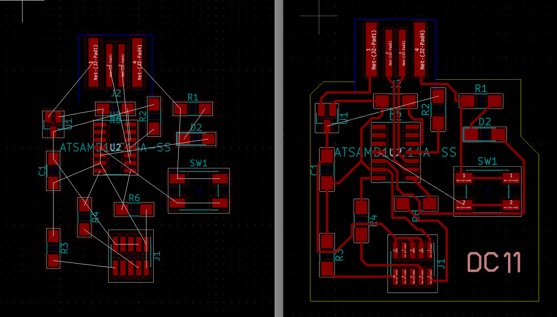
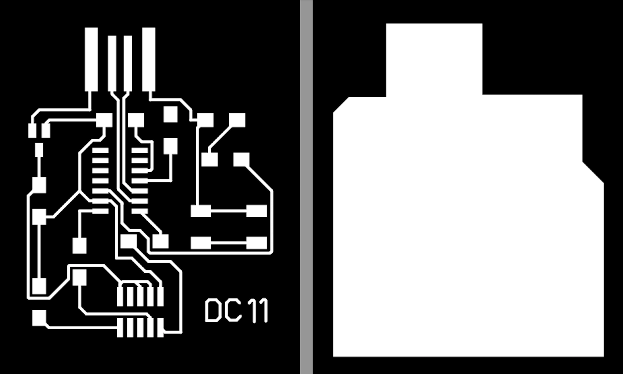
It wasn't until I milled this PCB that I realized that the traces were merging together. I will continue this work in anticipation of Week 06's assignment on embedded programming.
ATtiny412_trace ATtiny412_outline ATtiny412_schematic ATtiny412_pcb
DC11C_trace DC11C_outline DC11C_schematic DC11C_pcb