Week Three: Electronics Production
Our assignment this week was to follow the directions here to produce a "programmer", which is a board that programs other boards.
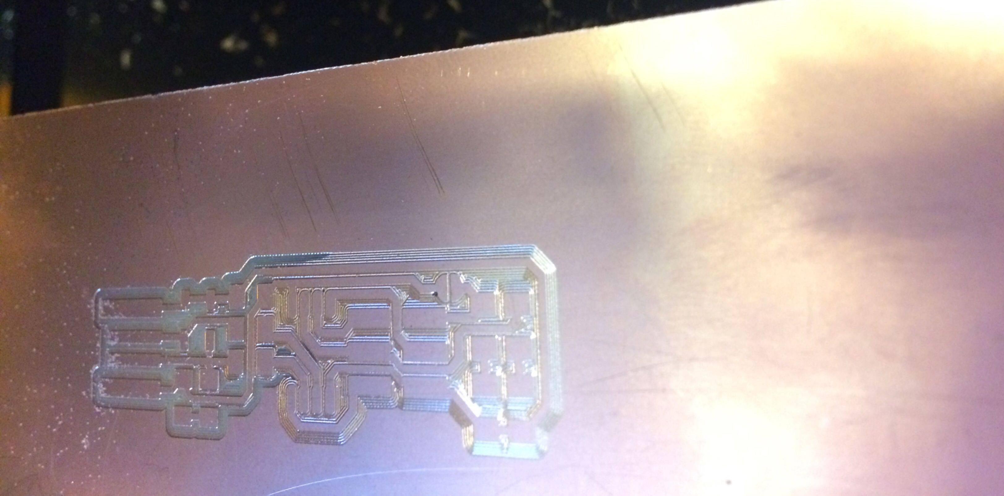
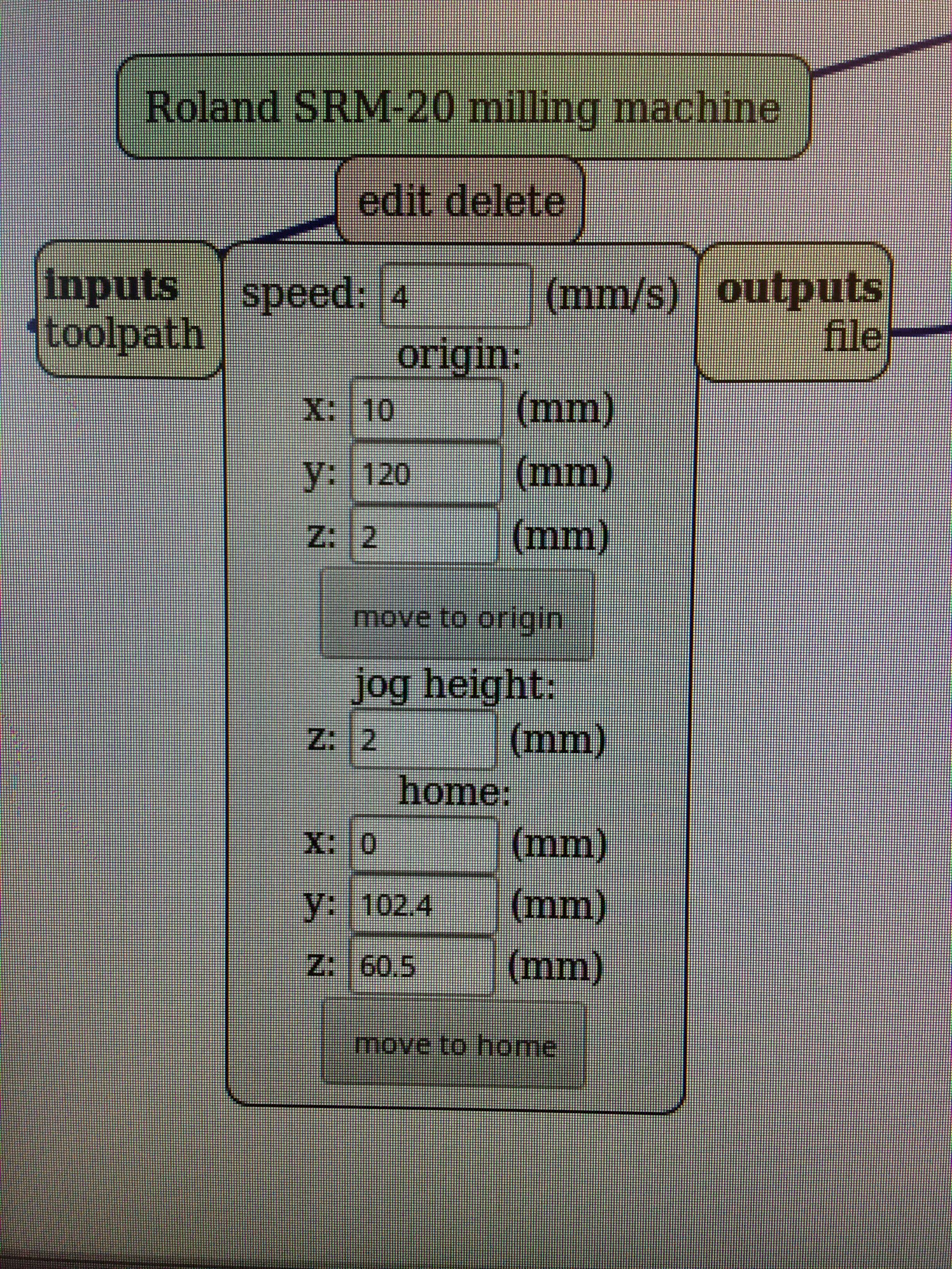
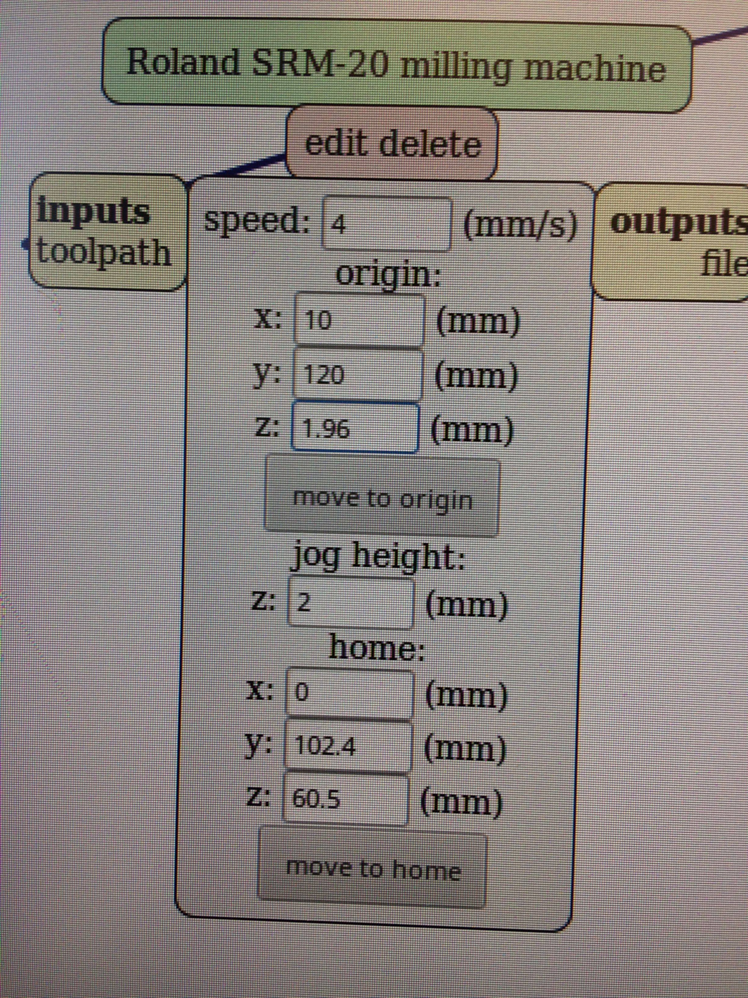
Milling the PCB
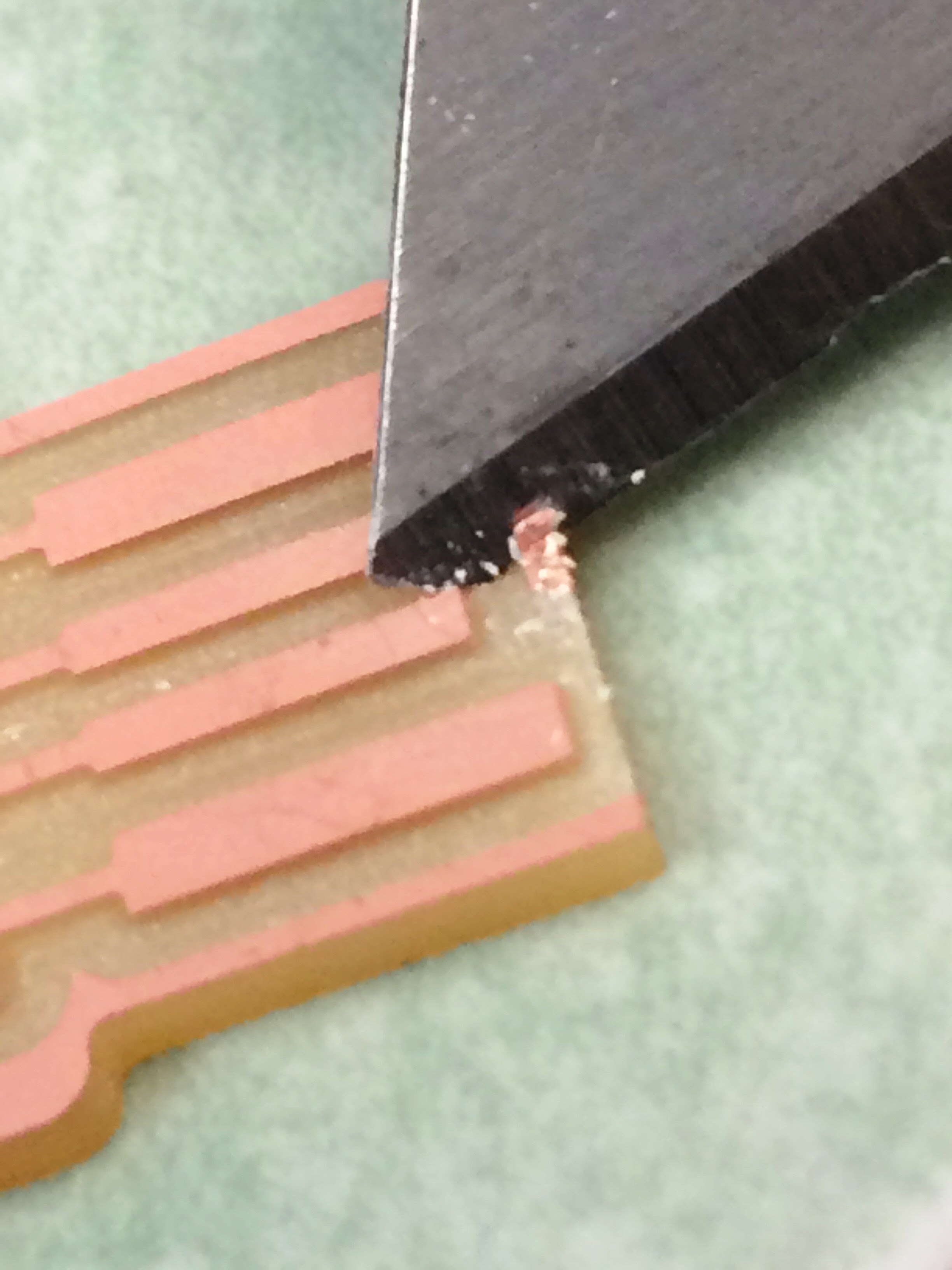
Some notes about the mill first. First goes the fixed bed, which is, as the name suggests, a part of the machine. Next there is a frame, and on top of that there is a sacrificial layer, and the board you're making is attached to that with double-sided stick-tape. The end-mill itself comes in 1/64" and 1/32" sizes; the former is used for for milling traces, and the latter is used for cutting outlines. The end-mill is held by a collet, which has a screw that is tightened by a very skinny screwdriver. The endmill is lowered onto the surface of the board, and cuts through the upper copper layer to mill out the traces.
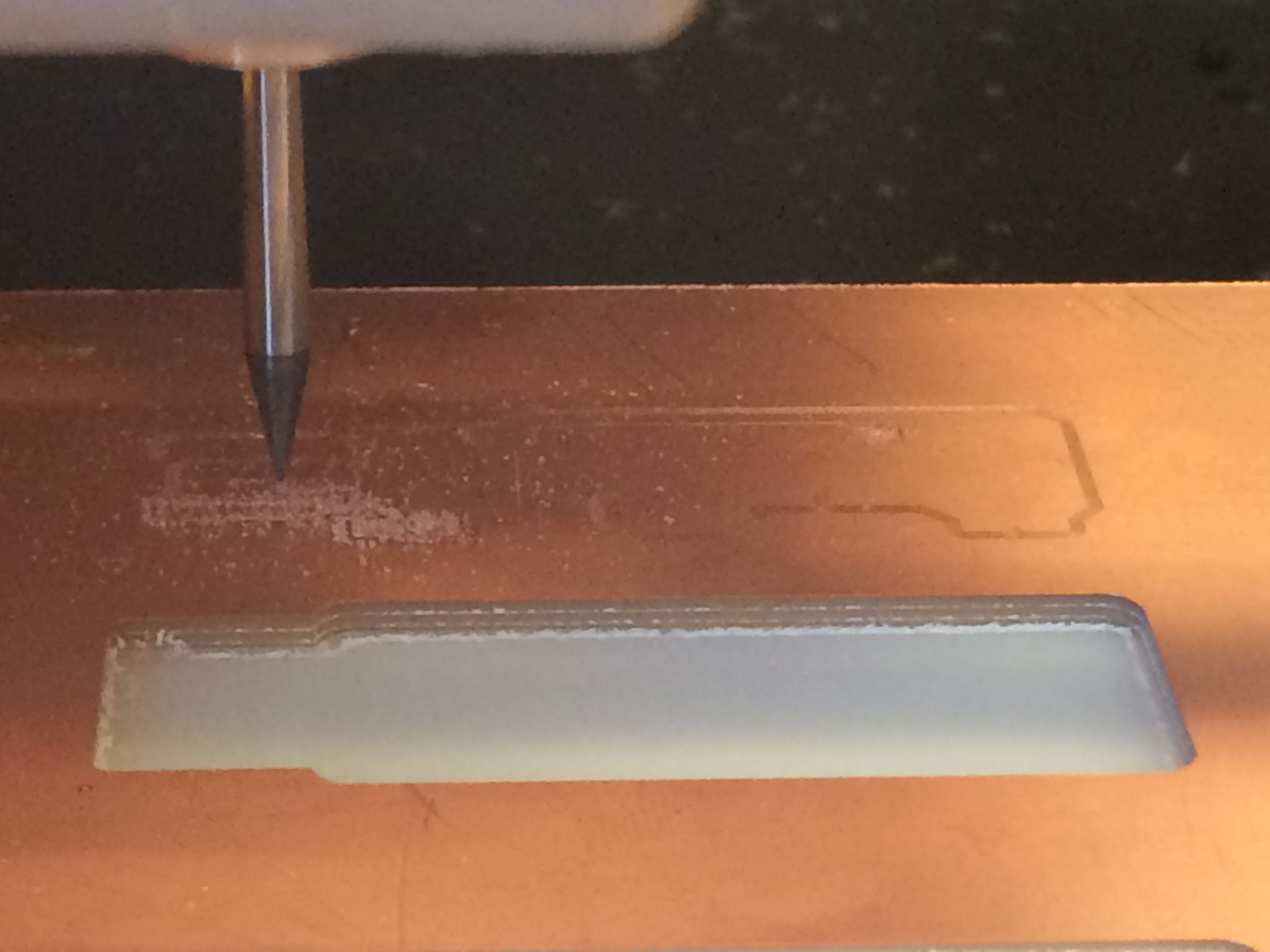
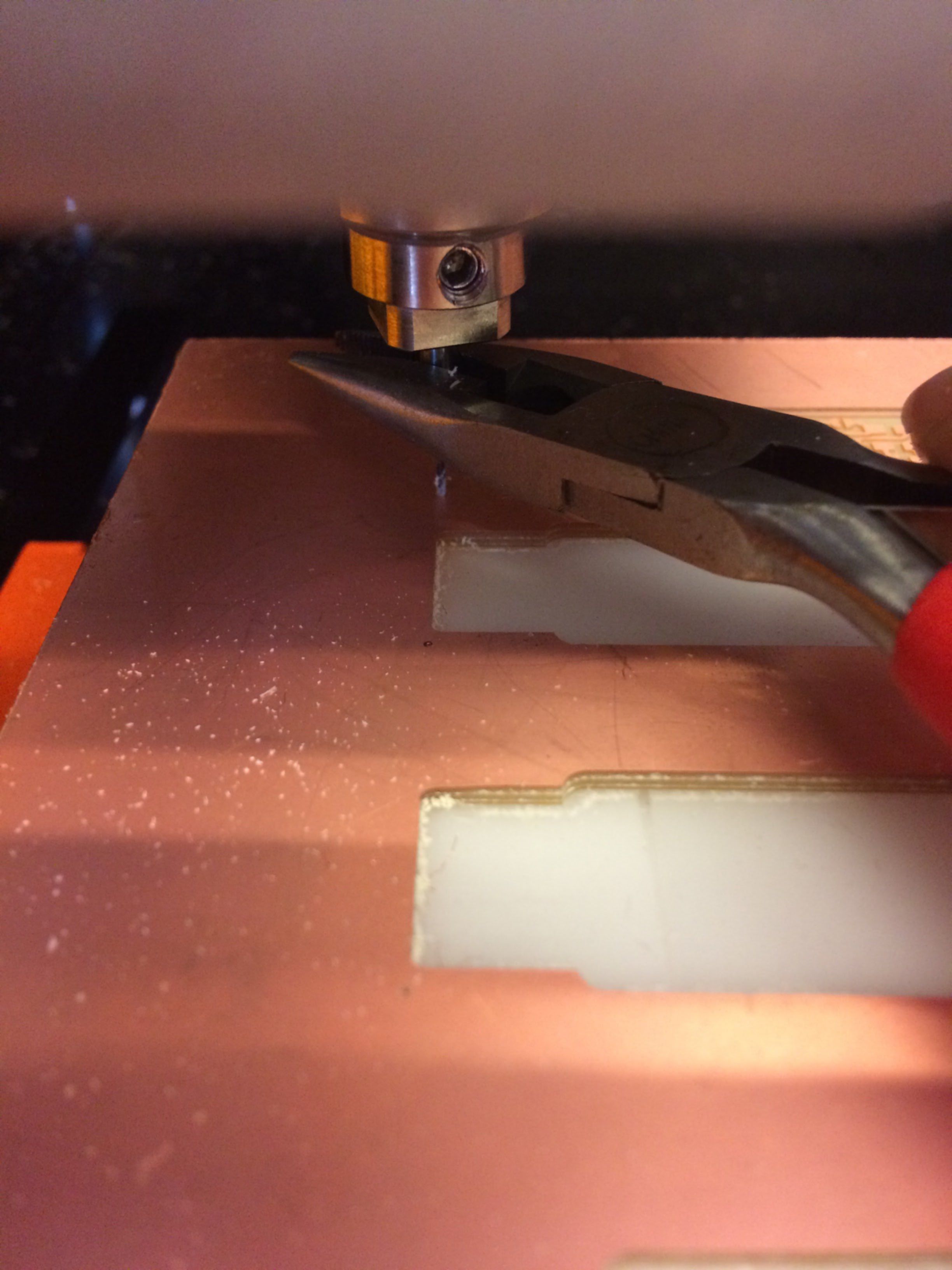
My first clue that something was that there was not nearly enough debris. The tip actually has to be pressed fairly hard against the surface of the copper in order to cut all the way through - which is, of course, the goal, since if there's copper left connecting the traces you cut to each other, the board turns into one big short. From one of the other students I picked up the technique of, before tightening the clamp, putting a pair of needle-nose pliers around the circular part of the bit, then pushing down on the handle of the pliers, forcing the bit lower.
This didn’t actually fix the entire problem.
Because the board was uneven, a bit height that worked fine for the left side of the board was not low enough to cut all the way through the copper on the right side of the board. Further pushing was clearly necessary. The TA informed me that there was an additional technique I could use: the clamp, when tightened, actually pulls the bit up slightly, undoing all the pushing you did earlier. Therefore, tighten the clamp with the screwdriver and push down with the pliers at the same time, to avoid losing all your progress.

Note for future students: If that still isn't enough, apparently you can adjust bit height settings from the mod application. Specifically, adjust the origin z-value by a very small amount - ~50 microns, or .002 inches, in the units used by mods - once the bit is in place, forcing it deeper into the copper.
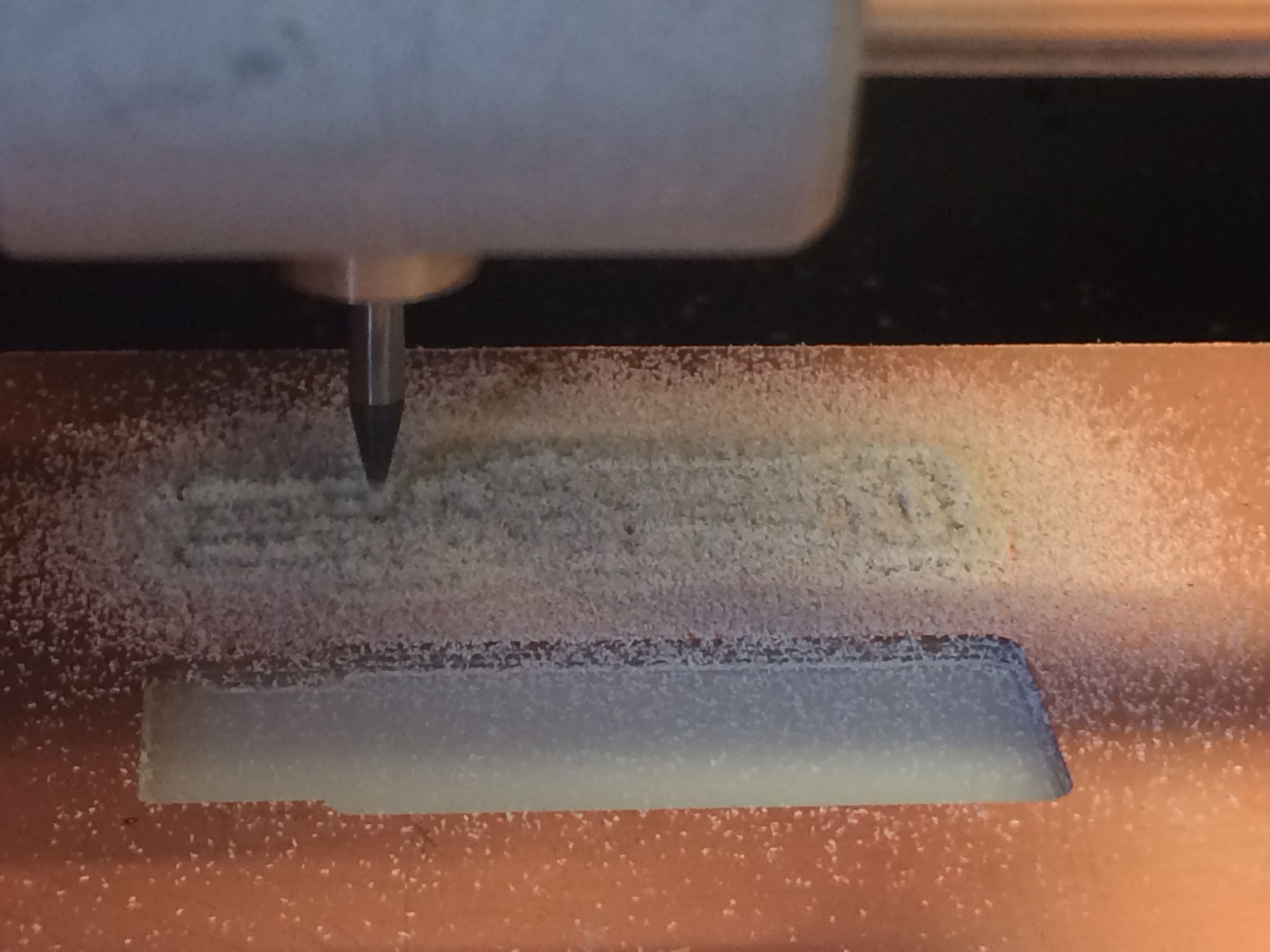
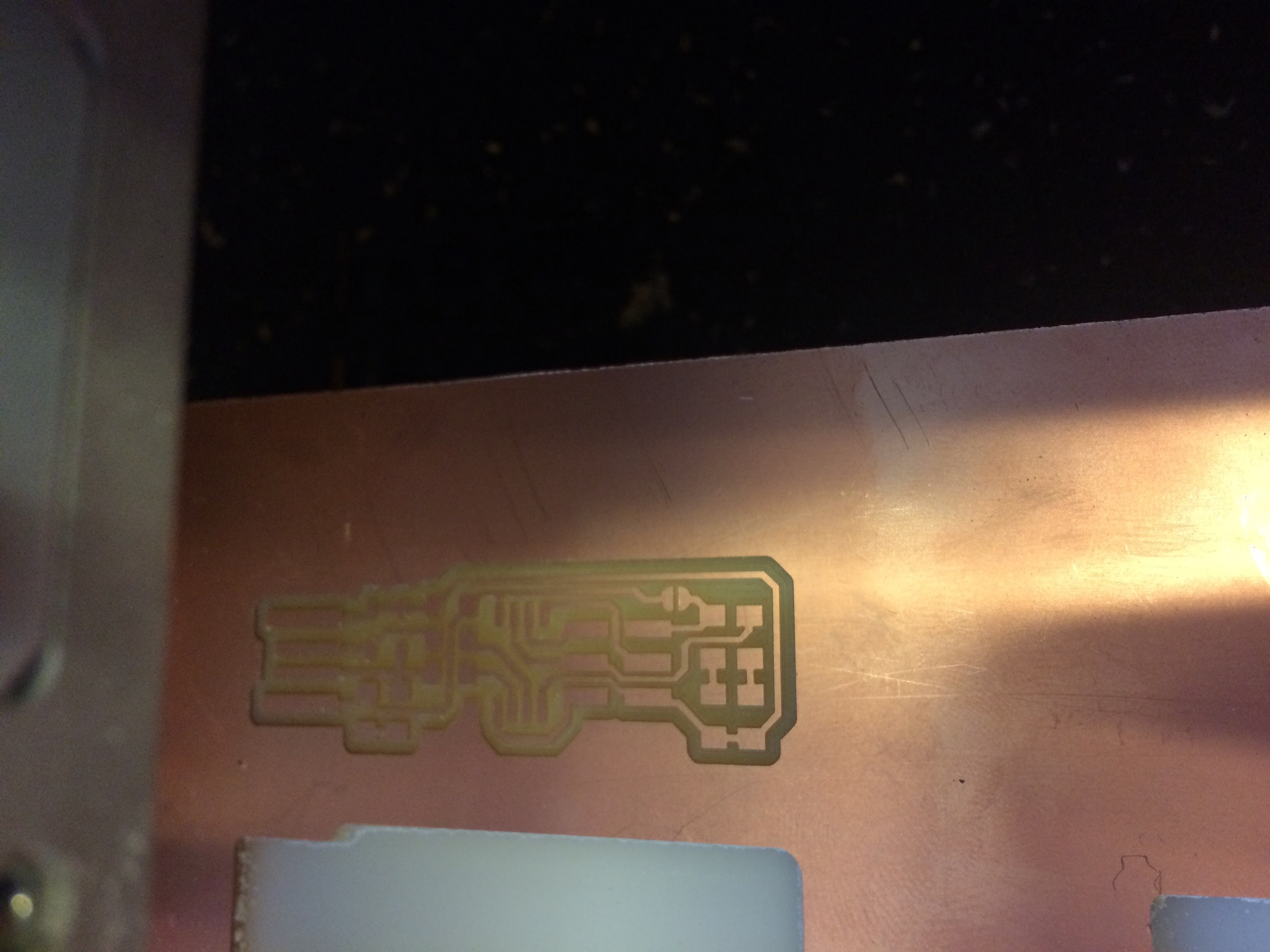
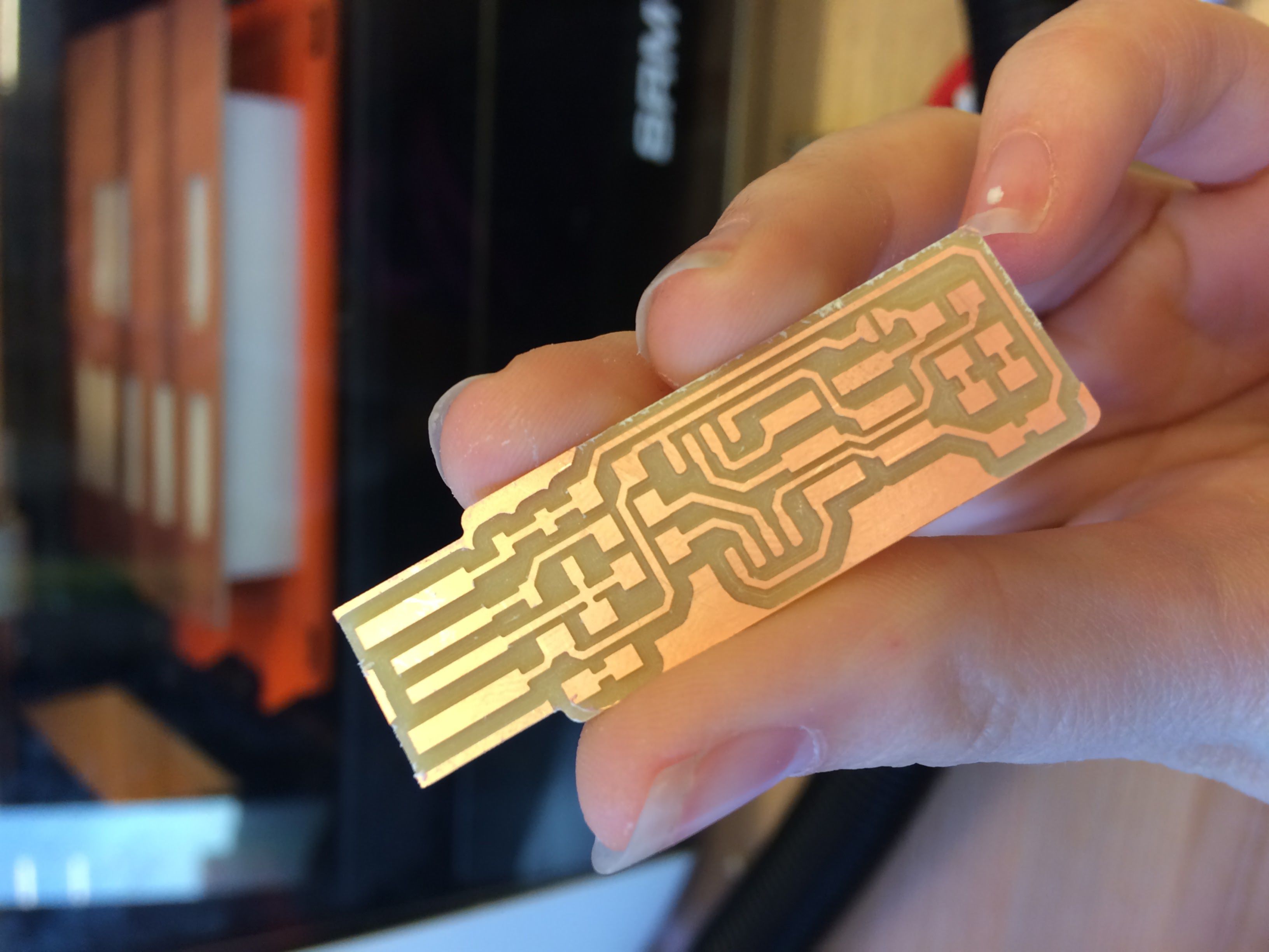
The last step for this part of the project is to remove the excess copper that might cause shorts, primarily across the front of the USB contacts.
Adding Components
The next part of the instructions concerned soldering all the correct electrical components to the board. The main thing I was confused by when going through these instructions was how I was supposed to tell which resistors and which diodes went where. The diagram of the PCB was labeled with R1, R2, R3, but not with which resistor R1 actually was.
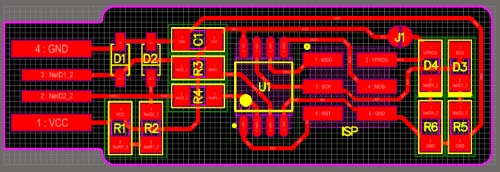
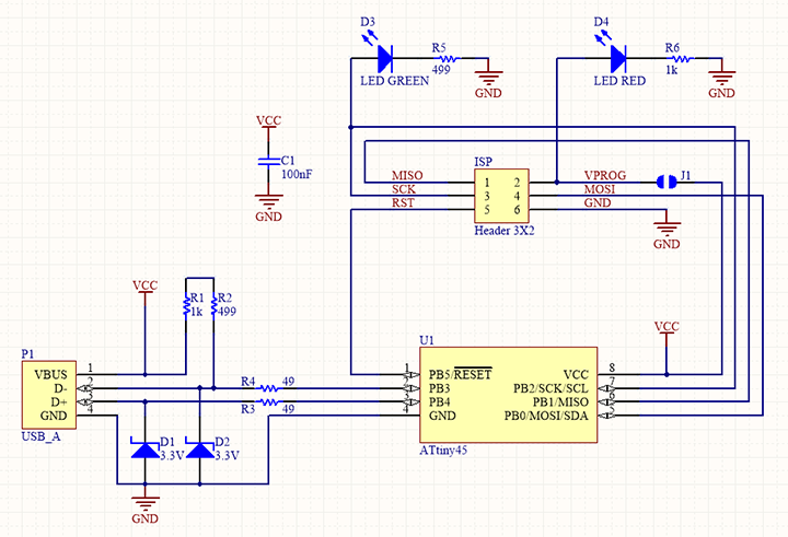
It was at this point that the TA pointed out that the R1, R2 and R3 were mirrored on the circuit diagram, which was, in fact, very well-labeled indeed.
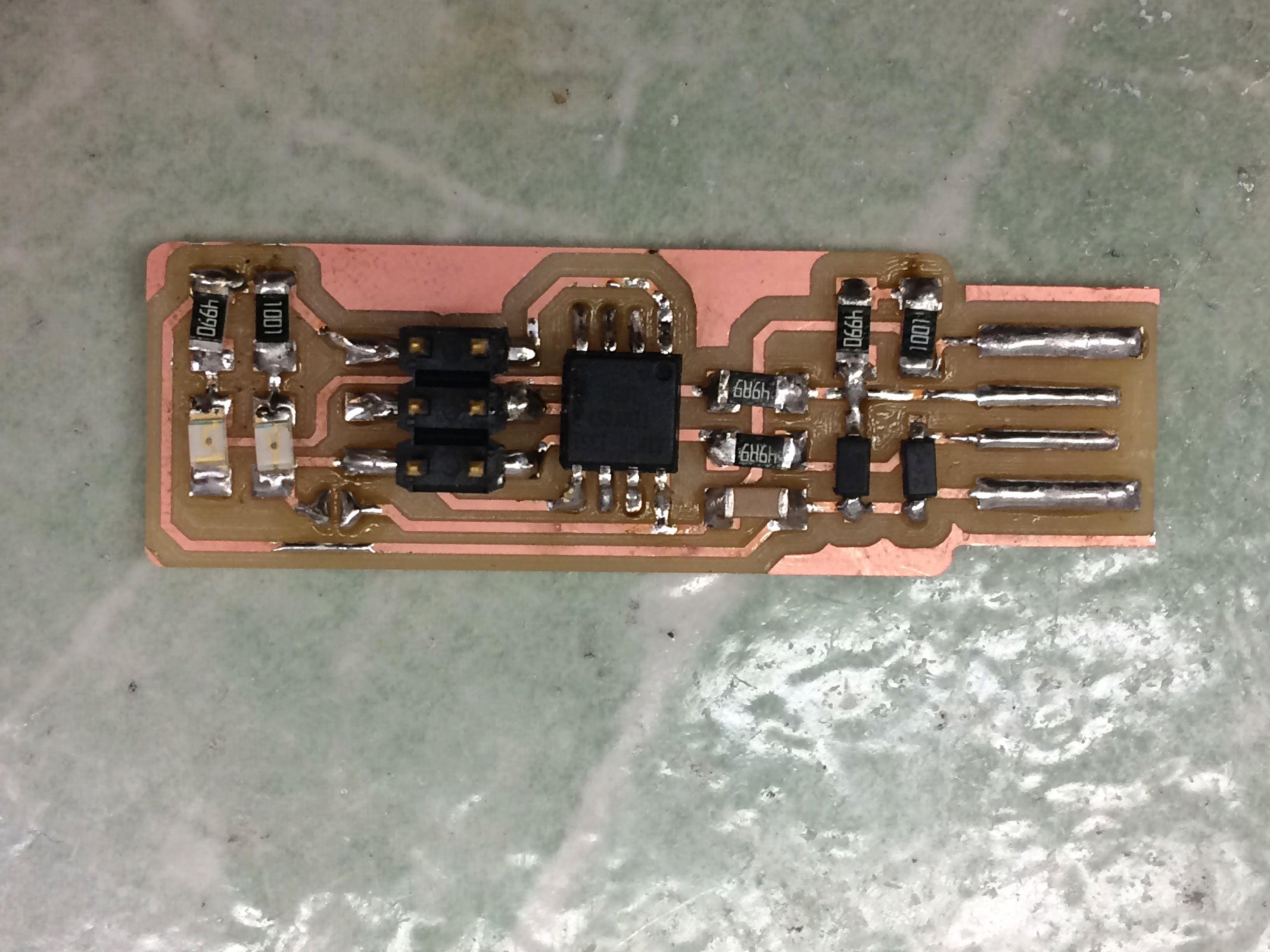
I then soldered. Only one note here, which is that you really do have to bulk up the USB contacts quite a bit in order to get a good connection once you've plugged this into the USB port. I went back twice and put more solder on, that's how important it is.
Programming the ATtiny45
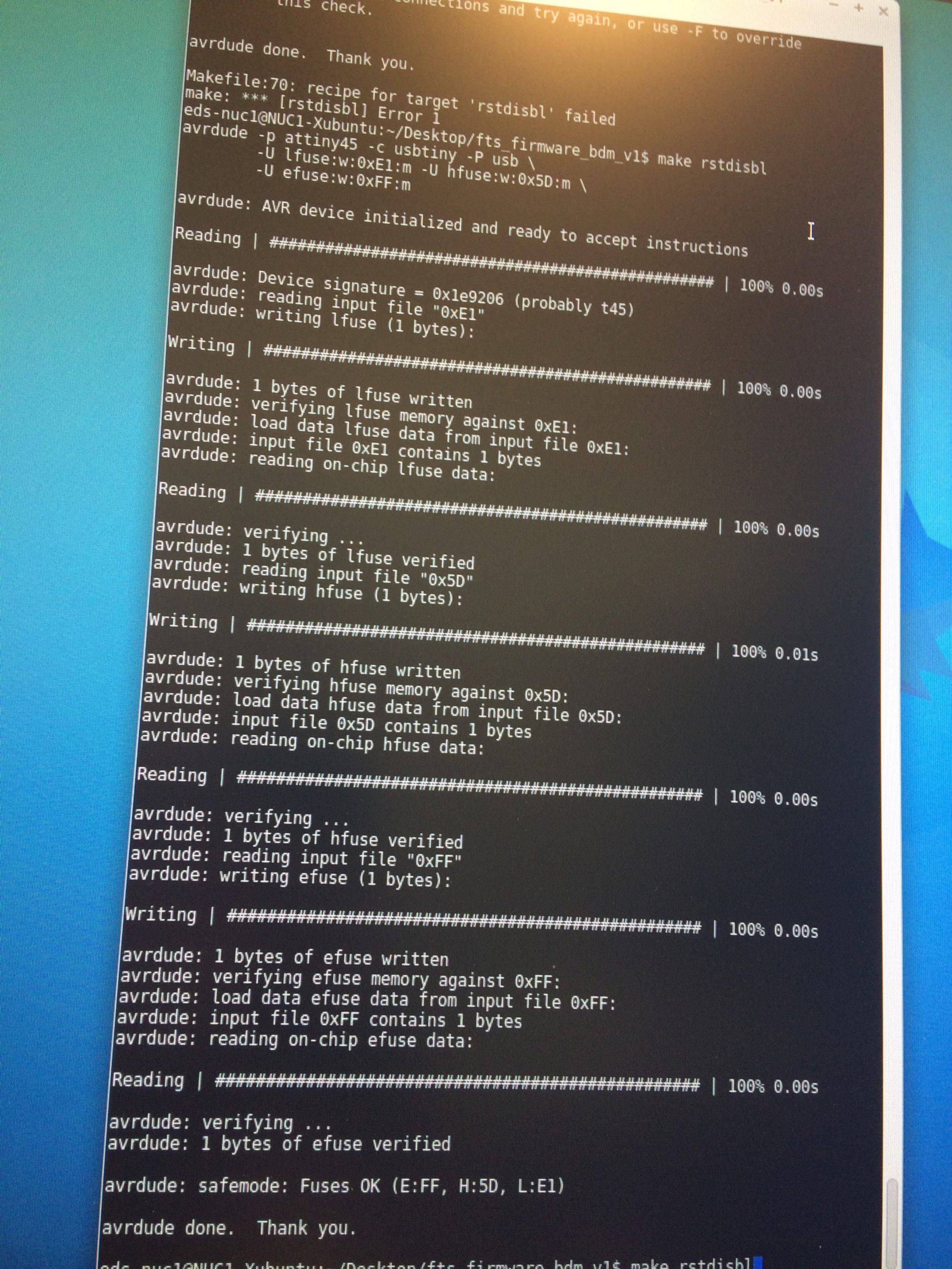
The ATtiny45 is the microcontroller that sits on this board. It needs to itself be programmed before it can be used to program other boards, and, in what seems vaguely like a circular dependency, you also need a programmer to program this board to program other boards. The only difficulty I had with this section of the project was that the instructions do not specify that the programmer needs to be plugged into the computer via USB as well as plugged into the ISP on the board. This is important, as the board isn't useable as a USB device until you program it. The last steps are to change this board from a programmee into a programmer: change the reset pin into a GPIO pin by running make rstdisbl, and then physically removing the solder bridge that previously connected the VCC and the Vprog pin.
That's all, folks! Tune in next week for 3D printing and scanning.