Week 3 - Electronics Production
Mill, Solder, and Test a Printed Circuit Board (PCB)
Milling
Milling is the bulk of the training but probably the most straightforward step. The training took about 3 hours in total: 1 hour/machine and 1 hour for soldering techniques. MIT Cypress Engineering Studio (EDS) has 2 milling machines --- Roland and Bantam --- but I prefer the latter for the following reasons. Firstly, the Roland exclusively uses MODS (a software developed by Neil Gershenfeld that offers process/machine specific file setup) to directly go from pngs to gcode and milling. In other words, if you have a mistake, Roland will not step you from milling. The Bantam setup, on the other hand, uses third party software like Eagle to bring up the gerber files (use vectors to show PCB layers) before starting the milling, which allows for errors to be caught. Using a third party software to render the gerber files first also allows milling optimizations to be made (though the Roland is typically faster at 10 min/1 sq inch and results in cleaner traces). Secondly, the Bantam is capable of milling multi-layer boards which is crucial to more complex boards, enabling certain I/O devices, and more. I, personally, hope to use a double-sided board for my final project where one side would use an input recorder to capture audio and the other side would have an amplified speaker for said capture. My only advice for the milling operation that I would give is to make sure your pngs are 1000 dpi when uploading to mods because it is a very easy mistake to make especially if you start customizing the designs and making your own boards.
Soldering
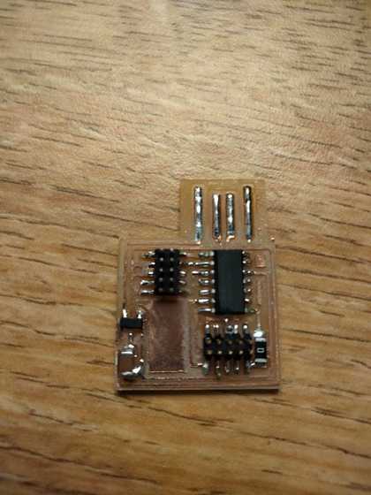
(Image 1) CMSIS-DAP.10.D11C PCB after soldering
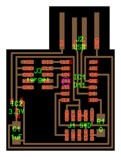
(Image 2) Example of an isolated pin
Soldering was a pain for me. My hands shake and I was pretty nervous because I didn't want to mill another board. It took me about 30 minutes to get in the groove, but some practice on a scrap board really helped. Also the realization that milling another board was hihgly unlikely, but even if it was, milling would be easier the second time helped ease my worries. My personal tips for soldering are as follows:
- When placing your iron to heat up the copper trace and lead before applying the solder, put the iron tip on the crevice between the lead and trace, not directly on the lead. In my experience, if you put the iron directly on the lead, the solder will go up the iron because the lead is hotter than the copper trace and the lead is connected to the iron. If you can, try to place the iron tip a little to the side of the lead still touching the trace so that the solder doesn't have to go around the iron tip.
- After removing the solder spool, make sure to keep your iron in the molten solder to let it flow, but more importanly you can move your iron to guide to solder down the trace.
- For isolated pins (see Image 2), rather than trying to feed the solder into a tight gap, you can try putting a small amount of solder on the iron and then have the solder melt onto the lead/trace.
- For solder removal in the case of a short (two traces connected via solder) and not a damaged component, I recommmend trying to first remove the solder by placing your iron into the gap as close to the component as possible and then dragging the solder outwards, which should push the solder into one of the two traces. If this doesn't work (likely because there is too much solder), try using the wicking tool. If this proves ineffective, I would try adding more solder to the gap to flood the excess out and then maybe trying the wick again.
Testing
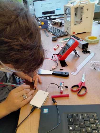
(Image 3) Anthony debugging with voltmeter
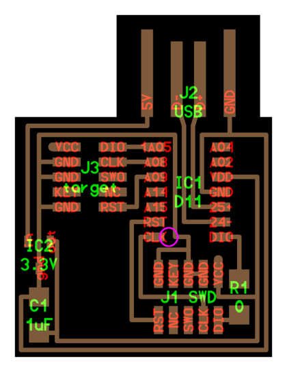
(Image 4) Milling artifact of connecting two traces
When I was testing, I thought it was just routine, but when that first test failed believe me my tone changed. I was nervous because I didn't want to mill another board. To debug, Anthony started using a voltmeter (see Image 3) to check the validity of my traces. One of the checks revealed that my clck on my chip was connected to the ground on the southern 5-pin array, but we weren't sure how. Then by looking at the proper angle, we found the smallest milling artifact --- a thin piece of copper --- was connecting two traces (see Image 4). Although it was unlucky, it goes to show that testing is super important, but more importantly, inspect your milled board very closely before soldering! To fix the issue, I used the hot air gun to lift the chip, wicked the soldered joint, cut the connection with an xacto knife (carefully as to not cut any other traces), used the hot air gun to reheat the solder and place the chip, and then resoldered some loose joints. After plugging into the computer and programming the board with the firmware binary, the PCB is now readable in the Arduino IDE! In short, given you have no idea what may have gone wrong, always closely compare your board to the schematic after milling to catch any shorts before soldering! If you want a smooth experience when using these PCBs to program other boards in 4 weeks, make sure to test!